

Global American 3304280 User Manual

User’s Manual
3304280

Table of Contents
Introducti on ............................................................................. 4
Specifications .......................................................................... 5
General Specifications .......................................................................................5
High Speed Multi I/O .... .......................................... ............................................. .5
Network Interface Controller ..............................................................................6
Display Controller ...............................................................................................6
Environmental and Power ..................................................................................6
Ordering Codes ........................................ ......................................................... . 8
Board Image ............................................................................9
Board Layout ......................................................................... 10
Jumper/Connector Quick Reference ...................................... 11
Jumper/Connector Quick Reference ...................................... 12
CMOS Jumper Settings.......................................................... 13
DOC Address Select .. ............................................................. 14
DOC Address Select (J2).. .................................. ........................ .................... . 14
Serial Port Selection (RS232C/422/485) .................................. 15
RS-422/485 Mode on COM2 .............................................................................15
LCD Inverter .......................................................................... 16
Watchdog Timer.................................................................... 17
Timeout Values .................................................................................................17
Timeout Table....................................................................................................17
Fast Ethernet Connectors ....................................................... 20
LAN Port ................... ................................. ......................... ................. ............. 20
LAN LED Indi cator on RJ-45 c onnect or .... ........................................................ 20
Power Connector................................................................... 21
Switches and Indicators .............. ................ ................ .......... 22
Interface Connectors HDD, FDD ............................ ................. 24
Floppy Disk Drive
Connector ........................................................................................................24
Enhanced IDE Connector .................................... ................... 25
2
3304280 User's Manual

Peripheral Port ...................................................................... 26
Parallel Port ......................................................................................................26
USB Ports............ ..................................................................... ........ ................27
SIR... ....... ........... ...... .................................................. .......... ........... .... ..............27
CRT SVGA .. ............................................... .......................................... .............28
PS/2 Keyboard & Mouse ................................................................................. .28
COM1 & COM2 for RS-232 C Port .... ......................... .......................................29
Compact Flash Connector ................................................................................30
Compact Flash Disk ............................................................... 31
The interfac e of Comp act Flas h socket is design ated to use IDE2 . .................. 31
Attent ion! .... .................. ......................................................... ......... .................. 31
Installation Instructions .....................................................................................31
Compact Flash card is "NOT HOT-SWAPPABLE". If the CF card is swapped in the
condition of system power-on, it will damage the CF card. ...... ............... .31
Audio Connector ............ .......................................... ........................................ 32
System Resources................................................................. 33
Flat Panel VGA ....................... ................ .......................... ..... 35
Flat Panel VGA ....................... ................ .......................... ..... 36
Flat Panel VGA ................ ........... .................... .............. ......... 37
LCD Type Selection ............................................................... 38
AWARD BIOS Setup ........ ................................... .................... 39
Setup Items ......................................................................................................39
Standard CMOS Setup .....................................................................................41
BIOS Features Setup ................ .......................................... ............................. 43
Chipset Features Setup .............................. ................................. .................... 46
Power Management Setup ...............................................................................48
PnP/PCI Configuration.......................................................................................49
Integrated Peripherals ......................................................................................50
POST Codes .......................................................................... 52
Howto : Flash the BIOS... ...... ..... ....................... ..................... 59
What if things go wrong . .. ........................................ ...................................... .60
Warranty....... ........................... ................................. ............. 61
3304280 User's Manual
3

Introduction
GAI's product of 3304280 is a 3.5” SBC with an on-board embedded
5x86 class CPU , NS Geode GX1-300 processor. With this board, system
engineers will be able to upgrade 386-based or 486-based to 586-level
without som e additional worri es, because a NS Geode GX1-30 0 processor
and 64MB SDRAM are mount ed on 3304280 . No longer worry about the
CPU installation , don
process or . And the f an is not necessary for NS Geode G x1-300 , the MTBF
worries will be reduced . DRAM on-board will improve the ability of the antivibration . 3304280 has the good reliability for system designer .
With its ultra low power, rich levels of integration, advanced multim edia
capabi lities and communic ation features, this board is an exciting opport unity
for System Int egrators and OEMs to devel op new generation prod ucts that
meet the desires and aspir at ions of t he 21th cent ury con sumers.
’t n
eed to set any jumpers of speed or volt age of
4
3304280 User's Manual

Specifications
General Specifications
•
CPU
: NS Geode GX 1 300 MHz MHz with FSB 33MHz.
•
Chipset
: NS CS5530A.
•
BIOS
: AW A RD® Flash BIOS
•
Green Function
APM
•
L1 Cache
•
L2 Cache
•
DRAM Memory
SODIMM (144-pin), Total of 320MB Memory
•
Enhanced IDE with UltraDMA
devices, Ultra DMA transf er 33 MB/sec. Two 44-pin (2.0 pitch) box
head er.
•
Watchdog Timer
loses control over the system.
•
Real-time Clock
backup of BIOS setup and BIOS default.
High Speed Multi I/O
•
Chipset
•
Serial Po rts
RS-232C/422/485 port COM2 (jumper selectable). Bot h with 16C550
compatible UART.
•
USB
: 2 onboard USB prots Ver 1.1.
•
SIR Interface
•
Floppy Disk Drive Interface
MB or 2.88 MB).
•
Bi-di rectional Parallel Port
•
Keyboard and Mouse Connectors
1 mini DIN) and onboard AT Keyboard port (6-pin box header)
•
Audio Chipset
Sound and Direct Sound 3D acceleration. (Line-in, CD Audio in, MIC in,
Speaker out)
: power saving supported in BIOS. DOZE / STANDBY
: Integ rat ed on CPU
: Integ rat ed on CPU
: Onboard 64MB SDRA M, and up to 256MB of SDRAM on
: supports 2 port and up to 4 ATAPI
: 1~127 S ec gen erates RESET when your application
: built-in chipset with lithium battery backup. CMOS data
: Winbond 83977F
: Two high speed RS-232C ports (COM1). One high speed
: onboard IrDA TX/RX port
: 2 floppy disk drives, 3½ " (720 KB, 1.44
: SPP, EPP and ECP mode.
: extern al PS/2 KB/ Mouse port (2-in-
: NS CS5530A, AC97 2.0 compliant, Multistream Direct
3304280 User's Manual
5

Networ k Interf ace Controller
•
Chipset
•
Connector
: Single Realtek 8139 C, 10/100 Mbps
: extern al RJ- 45 with LED s on connect or
Display Controller
•
Chipset
•
Display Type
(CS5530A) TFT LCD TV-Out (3304280VL including)
•
Connectors
•
Resolution
resoluti ons up to 1280x102 4 @ 8bpp or 102 4x768 @ 16bpp or
800x600 @ 24bpp.
colors or 1024x768 @ 16bit . Panel resolutions up to
1280x1024 @ 8bpp or 1024x768 @ 16bpp .
: SMI712(3304280/VLC), CS5530A(3304280/VL)
: CRT (VGA, SVGA, XGA, SXGA), 24-bit (SMI 712) and 16-bit
: external DB15 for CRT on-board
: >3304280/VLC CRT resolutions up to 1280x1024 @ 256
colors or 1204x768 @ 16bit or 800x60 0 @ 24bit . Panel
>3304280/ VL CRT resolu tions up to 1280x1024 @ 256
SSD Interfaces
•
DiskOnChip (DOC)
-
Package
-
Capacity
-
Data Reli ability
-
Memory Window
•
Compact Fl ash Card (CFC)
- Compact Flash Socket :
- Capacity
: Single Chip Flash Disk in 32-pin DIP JEDEC
: Up to 28 8 MByte
: ECC/EDC error correction
: 8 KByte
supports Type I/II CFC
: up to 512MB CFC
Env iron ment al and Power
•
Power Requirements
NS Geode GX1 300MHz wit h onboard 64 SDRAM)
•
Board Dimensions
•
Board Weight :
•
Operating Temperature
•
Operatin g Humidity
6
: +5 V @ 1.32 A (typical );(Low Power Embedd ed
: 145mm x 102mm
0.176kg
: 0 to 60°C (32 to 140°F)
: 0%~90%
3304280 User's Manual

Warning
Single Board Computers and their components contain very
delicate Integrated Circuits (IC). To protect the Single Board
Computer and its components against damage from static
electricity, you should always follow the following precautions
when handling it :
1. Discon nect your Single Board Comput er from the power sour ce
when you want to work on the inside
2. Hold the board by the edges and try not to touch the IC chips, leads
or circuitry
3. Use a grounded wrist strap when handling computer components.
4. Pl ace com ponents on a ground ed antist atic pad or on t he bag that
came with the Single Board Computer, whenever components are
separated from the system
3304280 User's Manual
7
PACKING LIST
3304280
1 x CD-ROM (driver)
3304280 Quick Installation
Before up and runn ing, please make sure the package contains all of above
accessories.
If any of the above item s is dam aged or missing, cont act your vendor
imm ediat el y.
Ordering Codes
3304280A
3.5" NS GX1 Module with 64MB on-board and one SODIMM up to 320 MB
SDRAM , SMI 712 Flat Panel / CRT V GA , Fast Ethernet , Audio
3304280B
3.5" NS GX1 Module with 64MB on-board and one SODIMM up to 320 MB
SDRAM , Flat Panel / CRT VGA , TV-out, Fast Ethernet , Audio
Note : Cable Kit is optional.
8
3304280 User's Manual
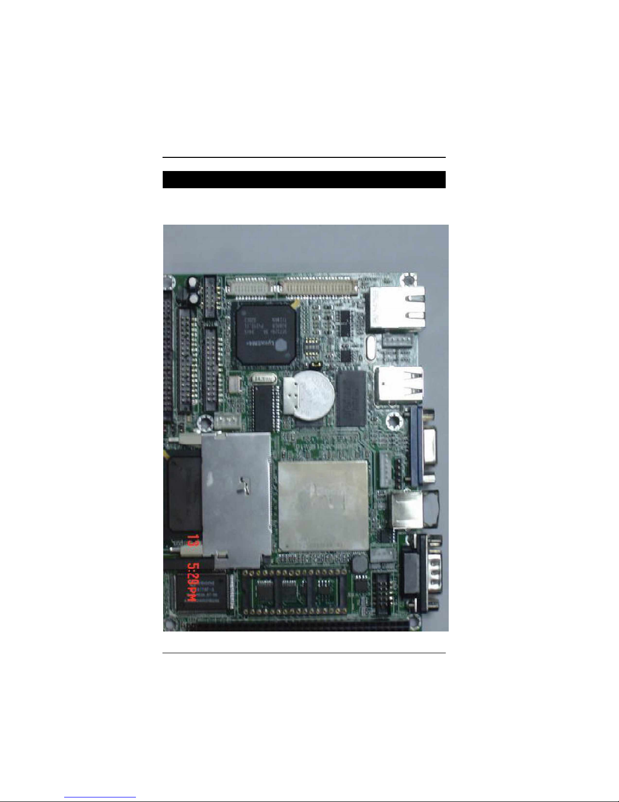
Board Image
3304280 User's Manual
9

Board Layout
IDE1 AUDIO
RES1
HLED1
PLED1
LPT1
FDD1
LCD3 LCD2
J1
ON
SW1
1 2 3 4
ATX1
Geode
GX1-
300B-55
JV9
LAN1
INV1
USB1
VGA1
KBM2
SIR1
KBM1
J6
COM1
J2
PWR1
10
DiskOnChip 2000
COM2
JFRT1 J5 PC104
3304280 User's Manual

Jumper/Connector Quick Reference
Jumpers Label Function
J1
J2 DOC Addr ess Select
J5 COM2 RS-232C / 422 / 485 Select ion
INV1
SW1 LCD type selection
J6 RS422/485 connector
Clear CMOS
(
INVERT ER
3304280 User's Manual
11

Jumper/Connector Quick Reference
Connectors
Label Function
VGA1
LCD2 LCD Co nn ect or
LCD3 LCD Co nn ect or
IDE1 Primary IDE Connector
CFD
USB1 USB Port 0,1
AUDIO
SIR1 Infrared (IR) Connector
KBM1 Keyboard and PS/ 2 Mouse (Mini Din)
KBM2 Keyboard and PS/2 Mouse
FDD1
LAN1 10/100M LAN1 Connector
LPT1 Parallel Port
COM1 RS-232C Serial Port (DSub-9)
COM2 RS-232C/422/485 Serial Port
PWR1 Sm all 4P Power Co nnect or
ATX1 ATX Power Connect or
DOC 2000 Disk On Chip 2000
RES1
PC104 ISA PC-104 Interface
PLED1
HLED1
JFRT1
SODIM1 SODIMM Socket
VGA Display Connector
Compact Flash Connector
Audio Interface Port
Floppy Drive Connector
Reset Switch
Power LED
HDD LED
Front Panel Connect or
12
3304280 User's Manual
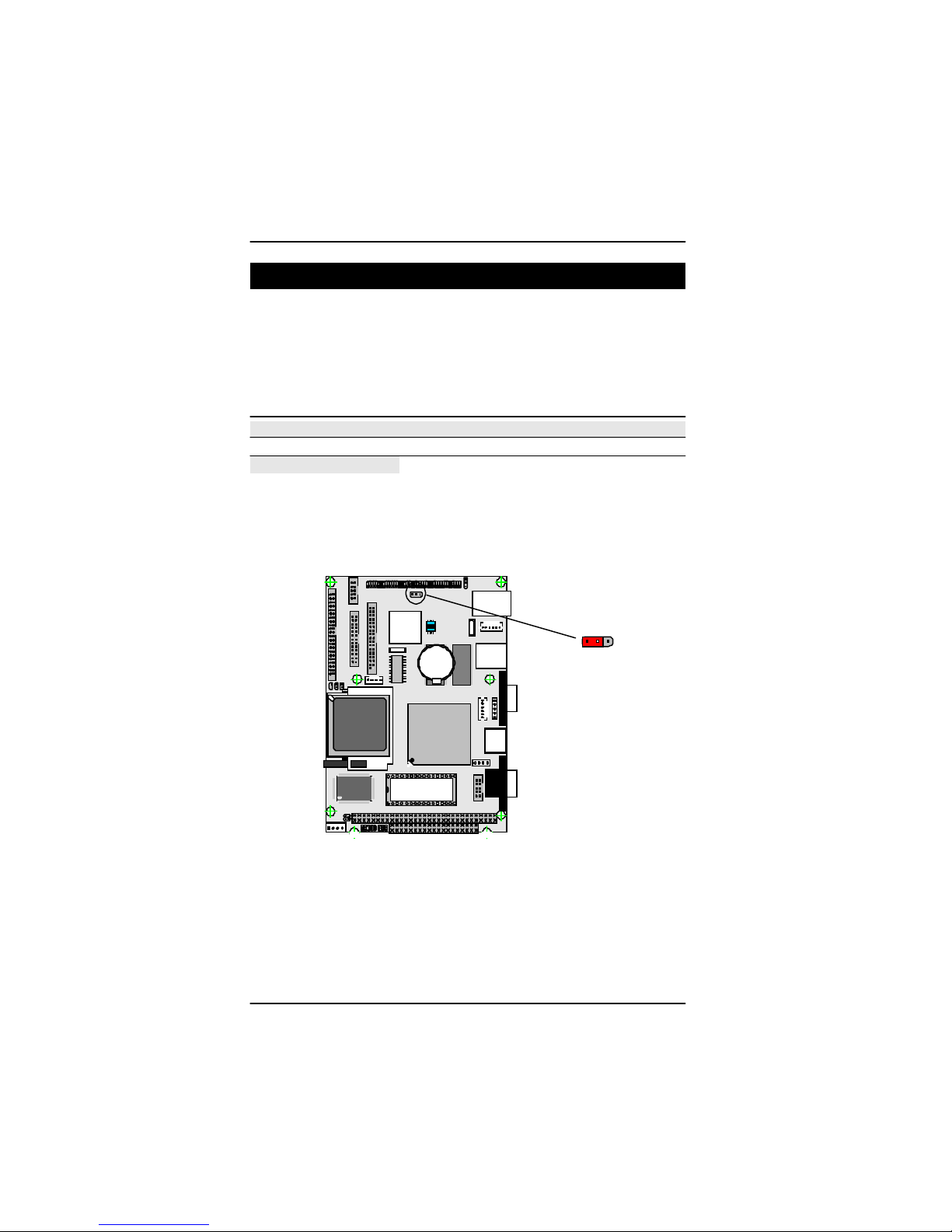
CMOS Jumper Settings
CMOS Operation (J1)
Type : J1: onboard 3-pin header
If the 3304280 refuses to boot due to inappropriate CMOS settings here i s how
to proceed to clear (reset) the CMOS to its default values.
CMOS Setup (J1)
Normal Operation
Clear CMOS
default setting 1-2 ON
*
ON
1 2 3 4
Geode
GX1-
DiskOnChip 2000
300B-55
J1 Statu s
1-2
ON
2-3
ON
1 2 3
J 1
3304280 User's Manual
13
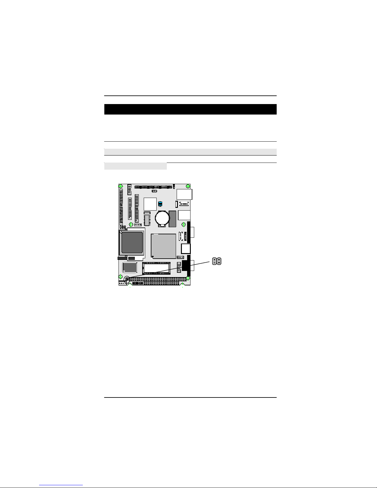
DOC Address Select
DOC Address Select (J2)
Type : J2: onboard 4-pin(2*2) header
Port Address
D800h
D000h
Disable
default s etting D800h
*
DiskOnChip 2000
ON
1 2 3 4
Geode
GX1-
300B -55
1-2 3-4
OFF OFF
ON
OFF
ON ON
3 1
4 2
14
3304280 User's Manual

Serial Port Sel ection (RS232C/42 2/485)
RS-232C/422/485 Mode select (J5)
Type : J5: onboard 6-pin(2*3) header
RS-422/48 5 Mode on COM2
The onboard COM2 port c an be configured to operate in RS-422 or RS-485
modes. RS-422 m odes differ in the way RX/TX is being handled. Jumper J5
switches between RS-232C or RS-422/485 mode. All of the RS-232C/422/485
modes are available on COM2.
COM2
Pin Defined: RS-232C RS-422 RS-485
Pin1 : DCD Tx+ RTx+
Pin2 : RXD Tx- RTxPin8 : CTS Rx+ x
Pin9 : RI Rx- x
J5 Selection
RS-232C
RS-422
RS-485
default s etting RS-232C
1-2 3-4 5-6
ON
OFF OFF
OFF
ON
OFF
OFF OFF
ON
ON
1 2 3 4
Geode
GX1-
*
DiskOnChip 2000
3304280 User's Manual
300B-55
2 4 6
1 3 5
15

RS-422/485 Output Port (J6)
Type : J6: onboard 4-pin header
PIN1 PIN2 PIN3 PIN4
RS-485 RS485+ RS485RS-422 RS485+ RS485- RS422+ RS422-
4 3 2 1
LCD Inverter
Connector : INV1
Typ e : Onboar d 5-pin mini boxheader
Pin
Description
1 +12 V 2
3
5
PPEN
GND
Default setting: 3.3V
ON
1 2 3 4
Geode
GX1-
300B-55
*
DiskOnChip 2000
16
Pin
Descriptio
n
GND
4
VEEP
3304280 User's Manual
1 2 3
J V9

Watchdog Timer
Watchdog Output
Th e onboar d watchd og tim er can be dis able by jum per set tin g or enabl e for
either reboot by system RESET .The Jumper is on the carrier board.
Even if enabl ed by jumper setti ng upon boot the watchdog tim er is alway s
inactive. To initial ize or refresh the watchdog timer writing of port 444H is
suffici ent. To disable the watchdog time read port 44H.
Status Action
Enable/refresh the Watchdog Timer I/O Wri te 444H
Disable the Watchdog Timer. I/ O Read 044H
After the watchdog timer has been initialize d by reading port 444H, it has to
be strobed at preconfigured int ervals to keep it from issuing a RESET or NMI.
The watchd og timer timeout intervals
are set by software programming.
Timeout Values
Timout values are programmed. The watc hdog timer supp orts 128 steps.
use the table on the next page t o find the hexidec imal value that needs to be
passed on to get the corr ect timer interval. Look subsequntly at the program
example how to pass the value to the watchdog tim er.
Timeout Table
Level Value Seconds Level Value Seconds Level Value Seconds
1 1 1 2 2 2 3 3 3
4 4 4 5 5 5 6 6 6
7 7 7 8 8 8 9 9 9
10 A 10 11 B 11 12 C 12
13 D 13 14 E 14 15 F 15
16 10 16 17 11 17 18 12 18
19 13 19 20 14 20 21 15 21
3304280 User's Manual
17

22 16 22 23 17 23 24 18 24
25 19 25 26 1A 26 27 1B 27
28 1C 28 29 1D 29 30 1E 30
31 1F 31 32 20 32 33 21 33
34 22 34 35 23 35 36 24 36
37 25 37 38 26 38 39 27 39
40 28 40 41 29 41 42 2A 42
43 2B 43 44 2C 44 45 2D 45
46 2E 46 47 2F 47 48 30 48
49 31 49 50 32 50 51 33 51
52 34 52 53 35 53 54 36 54
55 37 55 56 38 56 57 39 57
58 3A 58 59 3B 59 60 3C 60
61 3D 61 62 3E 62 63 3F 63
64 40 64 65 41 65 66 42 66
67 43 67 68 44 68 69 45 69
70 46 70 71 47 71 72 48 72
73 49 73 74 4A 74 75 4B 75
76 4C 76 77 4D 77 78 4E 78
79 4F 79 80 50 80 81 51 81
82 52 82 83 53 83 84 54 84
85 55 85 86 56 86 87 57 87
88 58 88 89 59 89 90 5A 90
91 5B 91 92 5C 92 93 5D 93
94 5E 94 95 5F 95 96 60 96
97 61 97 98 62 98 99 63 99
100 64 100 101 65 101 102 66 102
103 67 103 104 68 104 105 69 105
106 6A 106 107 6B 107 108 6C 108
109 6D 109 110 6E 110 111 6F 111
112 70 112 113 71 113 114 72 114
115 73 115 116 74 116 117 75 117
118 76 118 119 77 119 120 78 120
121 79 121 122 7A 122 123 7B 123
124 7C 124 125 7D 125 126 7E 126
127 7F 127
18
3304280 User's Manual

Programming Example
The following program is an examples of how to enable,
disable and refresh the Watchdog timer:
WDT_E N_RF equ 444H
WDT_DIS equ 044h
WT_En able push AX ; Save AX,DX
push DX
mov DX,WDT_EN_RF ; Enable Timer
mov AX,INTERVAL ; Set Timeout Value
out DX,AX
pop DX ; Restor e DX, AX
pop AX
ret
WT_Refresh push AX ; Save AX,DX
WT_Disable push AX ; Save AX,DX
WT_Disable push AX ; save AX,DX
push DX
mov DX,WDT_EN_RF ; Refresh Timer
mov AX,INTERVAL ; Set Timout Value
out DX,AX
pop DX ; Restor e DX, AX
pop AX
ret
push DX
mov DX,WDT_DIS ; Disabl e Timer
in AX,DX
pop DX ; Restor e DX, AX
pop AX
ret
push DX
mov DX,WDT_DIS ; Disabl e Timer
in AX,DX
pop DX ; restore DX,AX
pop AX
ret
3304280 User's Manual
19
 Loading...