


G-LINK GLT6400M16SLI-120TC, GLT6400M16SL-120TC, GLT6400M16LL-120TC Datasheet
G-LINK
GLT6400M16
Ultra Low Power 256k x 16 CMOS SRAM
May 2001(Rev. 1.1)
G-Link Technology Corporation
2701 Northwestern Parkway
Santa Clara, CA 95051, U.S.A.
G-Link Technology Corporation, Taiwan
6F No. 24-2, Industry E. RD. IV, Science Based
Industrial Park, Hsin Chu, Taiwan.
- 1 -
Features : Description :
∗ Low-power consumption.
-Active: 30mA Icc at 120ns.
-Stand by :
20 µA (CMOS input / output , LL)
5 µA (CMOS input / output, SL)
∗ Single +2.3V to 2.7V Power Supply.
∗ Equal access and cycle time.
∗ 120 ns access time.
∗ Tri-state output.
∗ Automatic power-down when
deselected.
∗ Multiple center power and ground pins
for improved noise immunity.
∗ Individual byte controls for both Read
and Write cycles.
∗ Industrial grade (-40°C ~ 85°C)
available.
∗ Available in 48-fpBGA/44L TSOPII.
∗ CE2 pin available for fpBGA only.
The GLT6400M16 is a low power CMOS Static
RAM organized as 262,144 words by 16 bits. Easy
memory expansion is provided by an active LOW
CE1 and OE pin and active HIGH CE2.
This device has an automatic power – down
mode feature when deselected. Separate Byte
Enable controls ( BLE and BHE ) allow individual
bytes to be accessed. BLE controls the lower bits
I/O0 – I/O7. BHE controls the upper bits I/O8 –
I/O15.
Writing to these devices is performed by taking
Chip Enable CE1 with Write Enable WE and byte
Enable ( BLE / BHE ) Low while CE2 remains
HIGH.
Reading from the device is performed by taking
Chip Enable CE1 with Output enable OE and byte
Enable ( BLE / BHE ) Low while Write Enable WE
and CE2 are held HIGH.
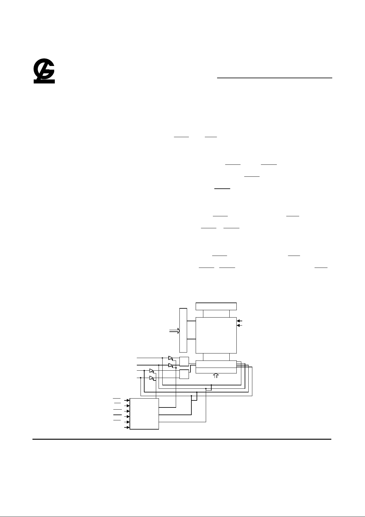
Function Block Diagram :
Row Select
Memory Array
2048 x 2048
Pre-Charge Circuit
I/O Circuit
Column Select
Data
Circuit
Data
Circuit
Vcc
Vss
WE
OE
BLE
BHE
CE1
I/O8 - I/O
15
I/O0 - I/O
7
Control
Logic
CE2
Column Address
Row Address
G-LINK
GLT6400M16
Ultra Low Power 256k x 16 CMOS SRAM
May 2001(Rev. 1.1)
G-Link Technology Corporation
2701 Northwestern Parkway
Santa Clara, CA 95051, U.S.A.
G-Link Technology Corporation, Taiwan
6F No. 24-2, Industry E. RD. IV, Science Based
Industrial Park, Hsin Chu, Taiwan.
- 2 -
BHE
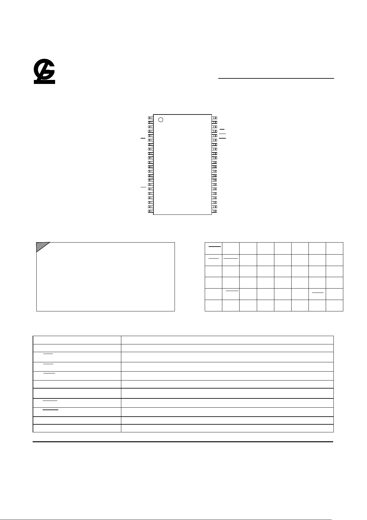
Pin Configurations :
GLT6400M16
A4
1
2
3
4
5
6
7
9
10
12
13
14
Vcc
8
15
16
17
18
19
20
21 24
25
26
27
28
29
30
31
32
33
35
36
37
38
39
40
41
42
43
44
CE1
I/O0
OE
BLE
22 23
3411Vcc
WE
A3
A2
A
1
A0
I/O1
I/O2
I/O3
Vss
I/O4
I/O5
I/O6
I/O7
A17
A16
A15
A14 A11
A10
A9
A8
NC
I/O8
I/O9
I/O10
I/O11
Vss
I/O12
I/O13
I/O14
I/O15
BHE
A7
A6
A5
A13 A12
48 Ball fpBGA :
1 2 3 4 5 6 7 8 A B C D E F G H
¡¡¡¡¡¡¡
¡
1
BLE
I/O9 I/O10 Vss Vcc I/O15 I/O16 NC
¡ ¡ ¡ ¡ ¡ ¡ ¡ ¡
2
OE
I/O11 I/O12 I/O13 I/O14 NC A8
¡ ¡ ¡ ¡ ¡ ¡ ¡ ¡
3
A0 A3 A5 A17 NC A14 A12 A9
¡ ¡ ¡ ¡ ¡ ¡ ¡ ¡
4
A1 A4 A6 A7 A16 A15 A13 A10
¡ ¡ ¡ ¡ ¡ ¡ ¡ ¡
5
A2
CE1
I/O2 I/O4 I/O5 I/O6
WE
A11
¡ ¡ ¡ ¡ ¡ ¡ ¡ ¡
6
CE2 I/O1 I/O3 Vcc Vss I/O7 I/O8 NC
Note : NC means no Ball.
Pin Descriptions:
Name
Function
A0 – A
17
Address Inputs
CE
1
and CE
2
Chip Enable Input
OE
Output Enable Input
WE
Write Enable Input
I/O0 – I/O
15
Data Input and Data Output
V
CC
2.5V Power Supply
BLE
Lower Byte Enable Input ( I/O0 to I/O7)
BHE
Higher Byte Enable Input ( I/O8 to I/O15)
GND Ground
NC No Connection
G-LINK
GLT6400M16
Ultra Low Power 256k x 16 CMOS SRAM
May 2001(Rev. 1.1)
G-Link Technology Corporation
2701 Northwestern Parkway
Santa Clara, CA 95051, U.S.A.
G-Link Technology Corporation, Taiwan
6F No. 24-2, Industry E. RD. IV, Science Based
Industrial Park, Hsin Chu, Taiwan.
- 3 -
Truth Table:
CE1
CE2
OE WE BLE BHE
I/O0-I/O7 I/O8-I/O15 Power Mode
HXXXX
X
High-Z High-Z
Standby
Deselected
XLXXX
X
High-Z High-Z
Standby
Deselected
XXXXH
H
High-Z High-Z
Standby
Deselected
LHHHL
X
High-Z High-Z
Active
Output Disabled
LHHHX
L
High-Z High-Z
Active
Output Disabled
LHLHL
H
Data Out High-Z
Active
Lower Byte Read
LHLHH
L
High-Z Data Out
Active
Upper Byte Read
LHLHL
L
Data Out Data Out
Active
Word Read
LHXLL
H
Data In High-Z
Active
Lower Byte Write
LHXLH
L
High-Z Data In
Active
Upper Byte Write
LHXLL
L
Data In Data In
Active
Word Write
Note ; X means don care. (Must be low or high state).
Absolute Maximum Ratings*
Parameter Symbol Minimum Maximum Unit
Voltage on Any Pin Relative to Gnd Vt -0.5 Vcc + 0.5 V
Power Dissipation P
T
- 1.0 W
Storage Temperature (Plastic) Tstg -55 +150
°C
Temperature Under Bias Tbias -25 +85
°C
*Note : Stresses greater than those listed above Absolute Maximum Ratings may cause permanent damage to the device.
This is a stress rating only and functional operation of the device at these or any conditions outside those indicated
in the operational sections of this specification is not implied. Exposure to absolute maximum rating conditions for
extended periods may affect reliability.
Recommended Operating Conditions ( TA = -25°C to 85°C )
Parameter Symbol Min Typ Max Unit
V
CC
2.3 2.5 2.7 V
Supply Voltage
Gnd 0.0 0.0 0.0 V
V
IH
2.0 - VCC+0.2 V
Input Voltage
V
IL
-0.2* - 0.6 V
* VIL min = -2.0V for pulse width less than tRC/2.
G-LINK
GLT6400M16
Ultra Low Power 256k x 16 CMOS SRAM
May 2001(Rev. 1.1)
G-Link Technology Corporation
2701 Northwestern Parkway
Santa Clara, CA 95051, U.S.A.
G-Link Technology Corporation, Taiwan
6F No. 24-2, Industry E. RD. IV, Science Based
Industrial Park, Hsin Chu, Taiwan.
- 4 -
DC Operating Characteristics ( Vcc=2.3 to 2.7V, T
A
= -25°C to 85°C )
120
Parameter Sym. Test Conditions
Min Max
Unit
Input Leakage Current
I
LI
VCC = Max,
Vin = Gnd to V
CC
- 1
µA
Output Leakage
Current
I
LO
CE
1
=VIH or CE2 = V
IH
VCC = Max, V
OUT
= Gnd to V
CC
- 1
µA
Operating Power
Supply Current
I
CC
CE
1
=VIL ,CE2 = V
IH
VIN=VIH or VIL, I
OUT
=0mA
- 5
mA
I
CC1
CE
1
=VIL ,CE2 = V
IH
I
OUT
= 0mA,
Min Cycle, 100% Duty
- 30 mA
Average Operating
Current
I
CC2
CE
1
=0.2V
CE2 = VCC – 0.2V
I
OUT
= 0mA,
Cycle Time=1µs, 100% Duty
- 5 mA
Standby Power Supply
Current(TTL Level)
I
SB
CE
1
=VIH or CE2 = V
IL
- 0.3 mA
GLT6400M16LL
20
µA
Standby Power Supply
Current (CMOS Level)
I
SB1
CE
1
≥ VCC-
0.2V or
CE2 ≤ 0.2V, f=0
VIN ≤ 0.2V or
VIN ≥ VCC-0.2V
GLT6400M16SL
-
5
µA
Output Low Voltage V
OLIOL
= 0.5 mA - 0.4 V
Output High Voltage V
OHIOH
= -0.5 mA 2.0 - V
Data Retention
Parameter Sym. Test Conditions Min. Max. Unit
VCC for Data retention
V
DR
1.0 - V
Data Retention Current
I
CCDR
- 4
µA
Chip Deselect to Data Retention Time
t
CDR
0 - ns
Operating Recovery Time
(2)
t
R
CE1
≥
VCC -0.2V
CE2 ≤ +0.2V
V
IN
≥
VCC -0.2V or
V
IN
≤ 0.2V
t
RC
- ns
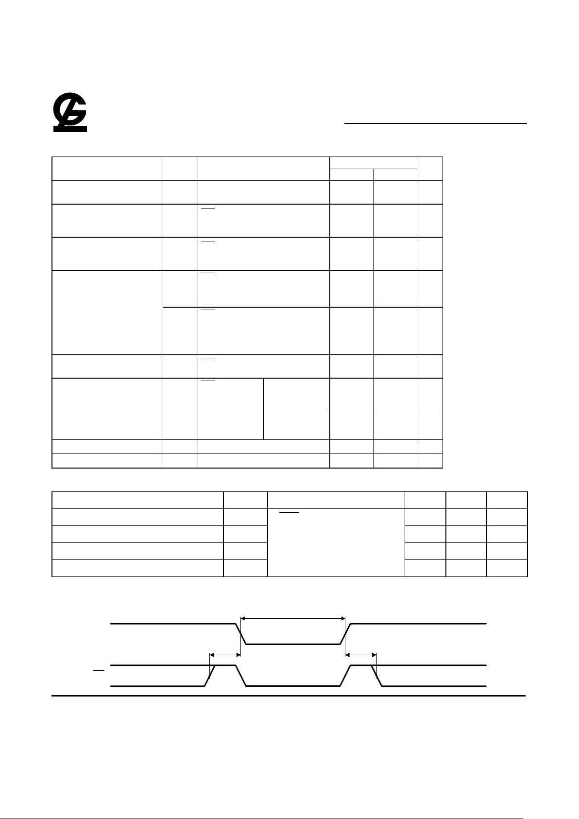
Data Retention Waveform (TA = -25°C to +85°C)
Data Retention Mode
Vcc
CE1
VDR
VDR >= 1.0V
tRtCDR
Vcc-typ
Vcc-typ
VIH
VIH