

G-LINK GLT6100L08SL-100TS, GLT6100L08SL-100ST, GLT6100L08LL-85TS, GLT6100L08LL-85ST, GLT6100L08LL-70TS Datasheet
...
G-LINK
GLT6100L08
Ultra Low Power 128k x 8 CMOS SRAM
Nov 2000(Rev. 02)
G-Link Technology Corporation
2701 Northwestern Parkway
Santa Clara, CA 95051, U.S.A.
G-Link Technology Corporation, Taiwan
6F No. 24-2, Industry E. RD. IV, Science Based
Industrial Park, Hsin Chu, Taiwan.
- 1 -
Features : Description :
∗ Low-power consumption.
-active: 30mA at 55ns.
-Stand by :
5 µA (CMOS input / output)
1 µA (CMOS input / output, SL)
∗ Single +2.7 to 3.3V Power Supply.
∗ Equal access and cycle time.
∗ 55/70/85/100 ns access time.
∗ Easy memory expansion with CE1 ,
CE2 and OE inputs.
∗ 2.0V data retention mode.
∗ TTL compatible, Tri-state input/output.
∗ Automatic power-down when
deselected.
The GLT6100L08 is a low power CMOS Static
RAM organized as 131,072 words by 8 bits. Easy
memory expansion is provided by an active LOW CE1
, an active HIGH CE2, an active LOW OE, and Tristate I/O’s. This device has an automatic powerdown mode feature when deselected.
Writing to the device is accomplished by taking
chip Enable 1 ( CE1 ) with Write Enable ( WE )
LOW, and Chip Enable 2 (CE2) HIGH. Reading from
the device is performed by taking Chip Enable 1 ( CE1
) with Output Enable ( OE ) LOW while Write Enable
( WE ) AND Chip Enable 2 (CE2) is HIGH. The I/O
pins are placed in a high-impedance state when the
device is deselected : the outputs are disabled during
a write cycle.
The GLT6100L08 comes with a 2V data retention
feature and Lower Standby Power. The GLT6100L08
is available in a 32-pin TSOPI / sTSOP / 48-fpBGA
packages.
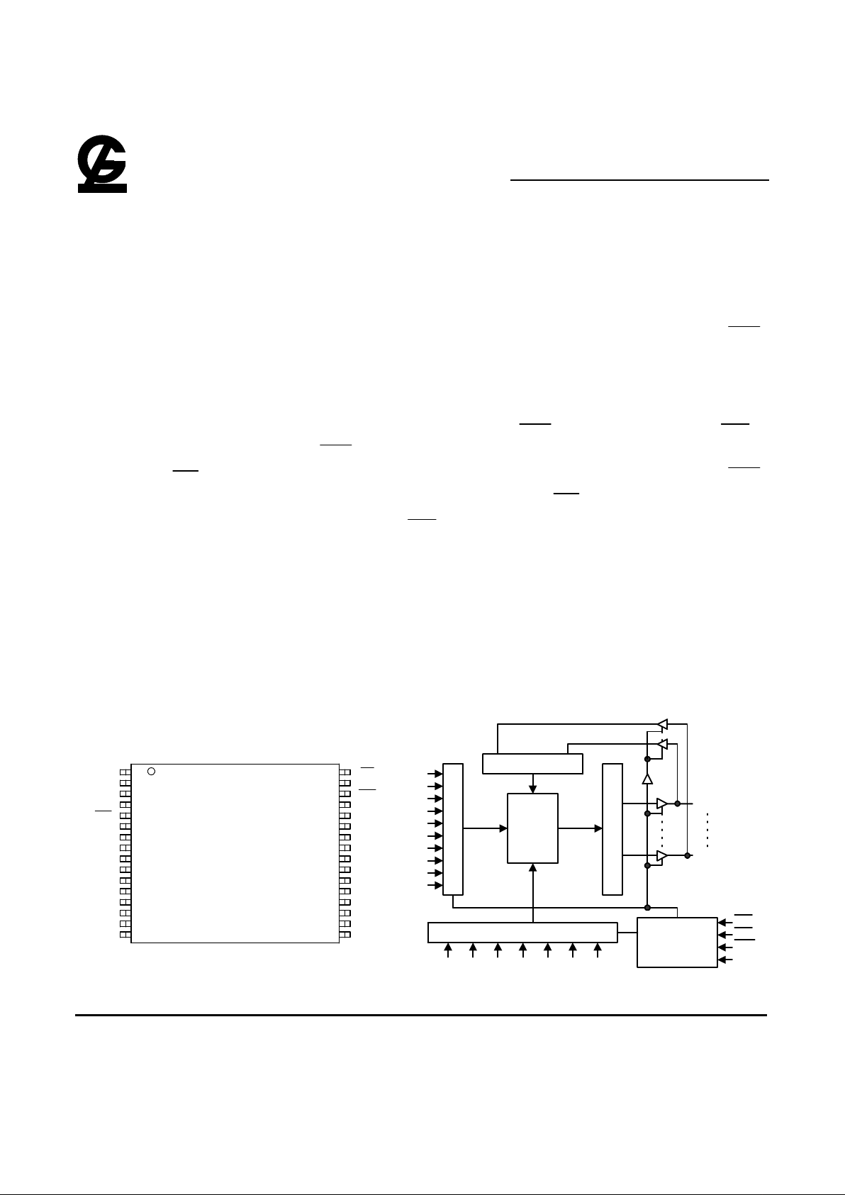
Pin Configurations :
GLT6100L08
A
16
A
7
1
2
3
4
5
6
8
9
10
11
12
13
22
21
19
18
17
26
25
2423GND
OE
A
10
14
27
28
I/O
8
I/O
7
20 A
0
7
WE
V
CC
NC
15
16
29
30
31
32A
11
A
9
A
8
A
13
CE
2
A
15
A
14
A
12
A
6
A
5
A
4
A
3
A
2
A1
I/O
1
I/O
2
I/O
3
I/O
4
I/O
5
I/O
6
CE
1
Function Block Diagram :
ROW DECODER
1024
x
1024
SENSE AMP
INPUT BUFFER
COLUMN DECODER
A10 A11A12A13A14A15A
16
A0
A1
A
2
A3
A
4
A
5
A6
A
7
A8
A9
CONTROL
CIRCUIT
OE
WE
CE1
CE2
I/O
8
I/O
1
G-LINK
GLT6100L08
Ultra Low Power 128k x 8 CMOS SRAM
Nov 2000(Rev. 02)
G-Link Technology Corporation
2701 Northwestern Parkway
Santa Clara, CA 95051, U.S.A.
G-Link Technology Corporation, Taiwan
6F No. 24-2, Industry E. RD. IV, Science Based
Industrial Park, Hsin Chu, Taiwan.
- 2 -
Pin Descriptions:
Name Function
A - A
0 16
Address Inputs
CE
1
and CE
2
Chip Enable Input
OE
Output Enable Input
WE
Write Enable Input
I O I O
0 7
/ /-
Data Input and Data Output
V
CC
3V Power Supply
GND Ground
NC No Connection
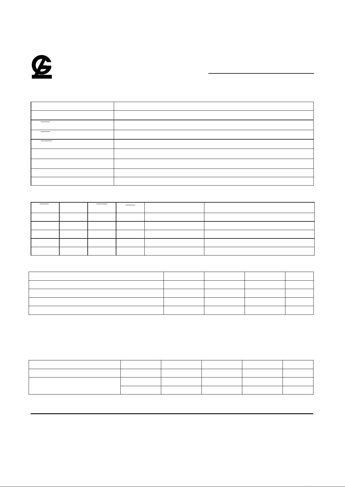
Truth Table:
CE
1
CE
2
WE
OE
Data Mode
HXXXHigh-Z
Standby
XLXXHigh-Z
Standby
LHHLData Out
Active, Read
LHHHHigh-Z
Active, Output Disable
LHLXData Out
Active, Write
Absolute Maximum Ratings*
Parameter Symbol Minimum Maximum Unit
Voltage on Any Pin Relative to Gnd Vt -0.5 4.6 V
Power Dissipation P
T
- 1.0 W
Storage Temperature (Plastic) Tstg -55 +150
°C
Temperature Under Bias Tbias -40 +85
°C
*Note : Stresses greater than those listed above Absolute Maximum Ratings may cause permanent damage to the device.
This is a stress rating only and functional operation of the device at these or any conditions outside those indicated
in the operational sections of this specification is not implied. Exposure to absolute maximum rating conditions for
extended periods may affect reliability.
Recommended Operating Conditions ( TA = -25°C to 85°C )**
Parameter Symbol Min Typ Max Unit
Supply Voltage V
CC
2.7 3.0 3.3 V
V
IH
2.2 - VCC+0.5 V
Input Voltage
V
IL
-0.5* - 0.6 V
* VIL min = -1.0V for pulse width less than tRC/2.
** For Industrial Temperature.
G-LINK
GLT6100L08
Ultra Low Power 128k x 8 CMOS SRAM
Nov 2000(Rev. 02)
G-Link Technology Corporation
2701 Northwestern Parkway
Santa Clara, CA 95051, U.S.A.
G-Link Technology Corporation, Taiwan
6F No. 24-2, Industry E. RD. IV, Science Based
Industrial Park, Hsin Chu, Taiwan.
- 3 -
DC Operating Characteristics ( Vcc=2.7V to 3.3V, T
A
=-25°C to 85°C )
55 70 85 100
Parameter Sym. Test Conditions
Min Max Min Max Min Max Min Max
Unit
Input Leakage Current
I
LI
VCC = Max,
Vin = Gnd to V
CC
1 1 1 1
µA
Output Leakage
Current
I
LO
CE
1
=VIH or CE2 = V
IH
VCC = Max, V
OUT
= Gnd to V
CC
1 1 1 1
µA
Operating Power
Supply Current
I
CC
CE
1
=VIL ,CE2 = V
IH
VIN=VIH or VIL, I
OUT
=0mA
3 3 3 3 mA
I
CC1
CE
1
=VIL ,CE2 = V
IH
I
OUT
= 0mA,
Min Cycle, 100% Duty
30 25 20 15 mA
Average Operating
Current
I
CC2
CE
1
=0.2V
CE2 = VCC – 0.2V
I
OUT
= 0mA,
Cycle Time=1µs, 100% Duty
3 3 3 3 mA
Standby Power Supply
Current(TTL Level)
I
SB
CE
1
=VIH or CE2 = V
IL
0.5 0.5 0.5 0.5 mA
GLT6100L08LL 5 5 5 5
µA
Standby Power Supply
Current (CMOS Level)
I
SB1
CE
1
≥ VCC-
0.2V or
CE2 ≤ 0.2V, f=0
VIN ≤ 0.2V or
VIN ≥ VCC-0.2V
GLT6100L08SL 1 1 1 1
µA
Output Low Voltage V
OLIOL
= 2 mA 0.4 0.4 0.4 0.4 V
Output High Voltage V
OHIOH
= 2 mA 2.4 2.4 2.4 2.4 V
Data Retention
Parameter Sym. Test Conditions Min. Max. Unit
VCC for Data retention
V
DR
1.0 - V
Data Retention Current
I
CCDR
5
µA
Chip Deselect to Data Retention Time
t
CDR
0 - ns
Operating Recovery Time
(2)
t
R
CE
1
≥
VCC -0.2V or
CE2 ≤ +0.2V,
V
IN
≥
VCC -0.2V or
V
IN
≤ 0.2V
t
RC
- ns

G-LINK
GLT6100L08
Ultra Low Power 128k x 8 CMOS SRAM
Nov 2000(Rev. 02)
G-Link Technology Corporation
2701 Northwestern Parkway
Santa Clara, CA 95051, U.S.A.
G-Link Technology Corporation, Taiwan
6F No. 24-2, Industry E. RD. IV, Science Based
Industrial Park, Hsin Chu, Taiwan.
- 4 -
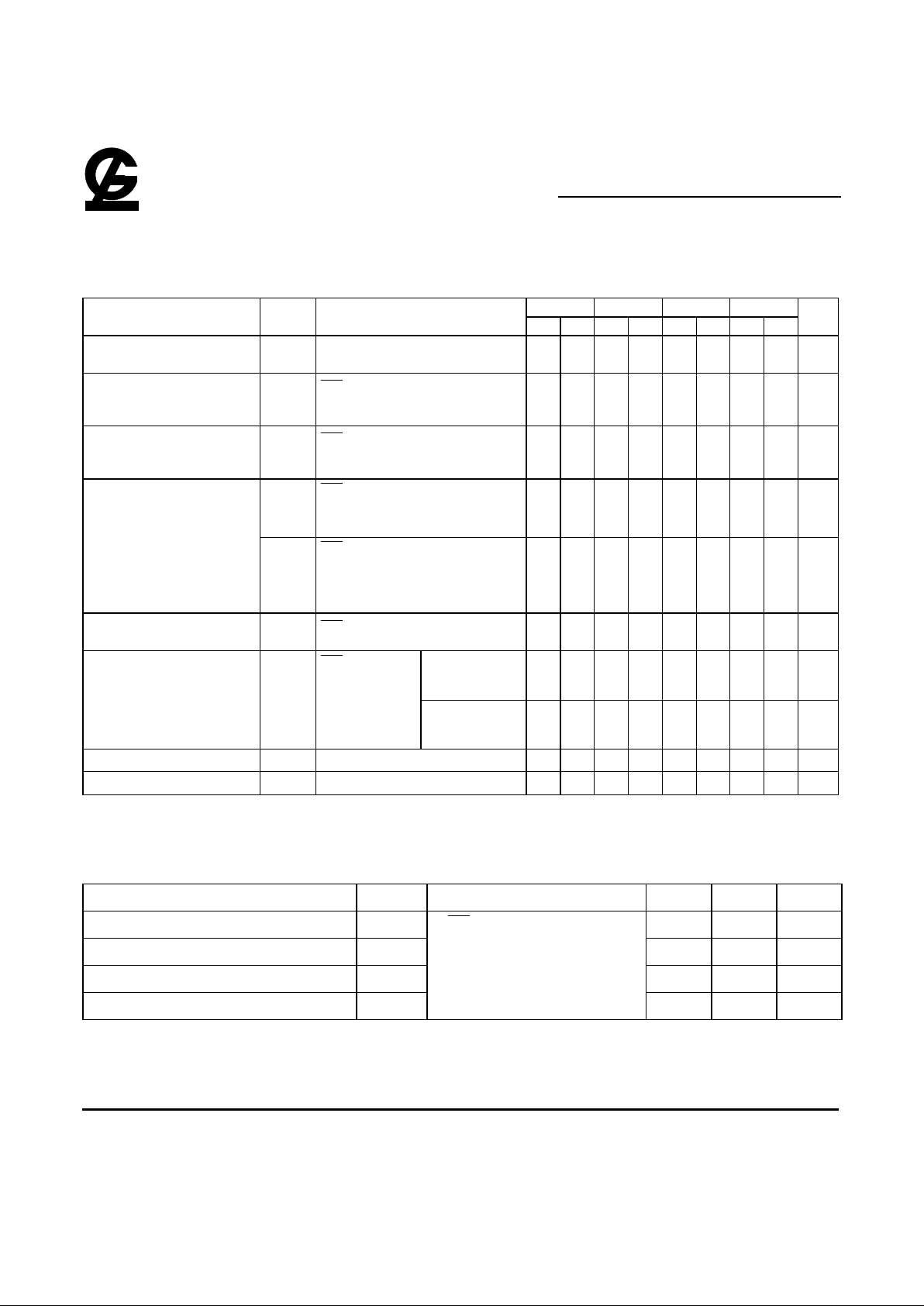
Data Retention Waveform (TA = -25°C to 85°C)
Data Retention Mode
Vcc
CE
VDR
VDR >= 1.0V
tRtCDR
2.7V
2.7V
V
IH
VIH
AC Test Conditions AC Test Loads and Waveforms
CL*
TTL
Output Load Condition *Including Scope and Jig Capacitance
70ns / 85ns CL = 30pf + 1TTL Load
Load 100ns / 120ns CL = 100pf + 1TTL Load
Read Cycle
(3,9)
( Vcc=2.7V to 3.3V, TA =-25°C to 85°C )
55 70 85 100
Parameter Symbol
Min Max Min Max Min Max Min Max
Unit Note
Read Cycle Time t
RC
55 70 85 100 ns
Address Access Time t
AA
55 70 85 100 ns
Chip Enable Access Time t
ACE
55 70 85 100 ns
Output Enable Access Time t
OE
35 40 40 50 ns
Output Hold from address Change t
OH
10 10 10 10 ns
Chip Enable to Output in Low-Z t
CLZ
10 10 10 10 ns 4,5
Chip Disable to Output in High-Z t
CHZ
25 30 35 40 ns 3,4,5
Output Enable to Output in Low-Z t
OLZ
5 5 5 5 ns
Output Disable to Output in High-Z t
OHZ
25 25 30 35 ns 4,5
Power-Up Time t
PU
0 0 0 0 ns 3,4,5
Power-Down Time t
PD
55 70 85 100 ns
Input Pulse Levels 0.6V to 2.2V
Input Rise and Fall Time
Input and Output Timing
Reference Level
5 ns
1.4V

G-LINK
GLT6100L08
Ultra Low Power 128k x 8 CMOS SRAM
Nov 2000(Rev. 02)
G-Link Technology Corporation
2701 Northwestern Parkway
Santa Clara, CA 95051, U.S.A.
G-Link Technology Corporation, Taiwan
6F No. 24-2, Industry E. RD. IV, Science Based
Industrial Park, Hsin Chu, Taiwan.
- 5 -
Timing Waveform of Read Cycle 1
(3,6,7,9)
(Address Controlled)
DOUT
tAA tOH
tRC
Data Valid
Address
Timing Waveform of Read Cycle 2
(5,6,8,9)
( CE1 Controlled)
t
OE
t
RC
Data Valid
CE1
t
OHZ
t
CHZ
t
PD
50%
50%
t
OLZ
t
ACE
t
CLZ
t
PU
Supply Current
OE
D
OUT
I
CC
I
SB
Timing Waveform of Read Cycle 1
(3,6,8,9)
(CE2 Controlled)
t
OE
t
RC
Data Valid
CE2
t
OHZ
t
CHZ
t
PD
50%
50%
t
OLZ
t
ACE
t
CLZ
t
PU
Supply Current
OE
D
OUT
I
CC
I
SB

G-LINK
GLT6100L08
Ultra Low Power 128k x 8 CMOS SRAM
Nov 2000(Rev. 02)
G-Link Technology Corporation
2701 Northwestern Parkway
Santa Clara, CA 95051, U.S.A.
G-Link Technology Corporation, Taiwan
6F No. 24-2, Industry E. RD. IV, Science Based
Industrial Park, Hsin Chu, Taiwan.
- 6 -
Write Cycle
(3,9)
( Vcc=2.7V to 3.3V, TA = -25°C to 85°C )
55 70 85 100
Parameter Symbol
Min Max Min Max Min Max Min Max
Unit Note
Write Cycle Time t
WC
55 70 85 100 ns
Chip Enable to Write End t
CW
45 60 70 80 ns
Address Setup to Write End t
AW
45 60 70 80 ns
Address Setup Time t
AS
0 0 0 0 ns
Write Pulse Width t
WP
45 50 60 70 ns
Write Recovering Time t
WR
0 0 0 0 ns
Data Valid to Write End t
DW
25 30 35 40 ns
Data Hold Time t
DH
0 0 0 0 ns
Write Enable to Output in High-Z t
WZ
25 30 35 40 ns
Output Active from Write End t
OW
5 5 5 5 ns
Timing Waveform of Write Cycle 1
(10,11)
( WE Controlled)
tWP
tAW
WE
tWC
tWR
tAS
t
DW
t
DH
tOW
tWZ
Data Valid
Address
DIN
DOUT

G-LINK
GLT6100L08
Ultra Low Power 128k x 8 CMOS SRAM
Nov 2000(Rev. 02)
G-Link Technology Corporation
2701 Northwestern Parkway
Santa Clara, CA 95051, U.S.A.
G-Link Technology Corporation, Taiwan
6F No. 24-2, Industry E. RD. IV, Science Based
Industrial Park, Hsin Chu, Taiwan.
- 7 -
Timing Waveform of Write Cycle 2
(10,11)
( CE1 Controlled)
tAW
WE
tWC
tWR
tDW tDH
Data Valid
Address
DIN
tAS tCW
t
WP
tWZ
CE1
DOUT
Timing Waveform of Write Cycle 1
(10,11)
(CE2 Controlled)
t
AW
WE
tWC
t
WR
tDW tDH
Data Valid
Address
D
IN
tAS tCW
tWP
tWZ
CE2
DOUT
G-LINK
GLT6100L08
Ultra Low Power 128k x 8 CMOS SRAM
Nov 2000(Rev. 02)
G-Link Technology Corporation
2701 Northwestern Parkway
Santa Clara, CA 95051, U.S.A.
G-Link Technology Corporation, Taiwan
6F No. 24-2, Industry E. RD. IV, Science Based
Industrial Park, Hsin Chu, Taiwan.
- 8 -
Notes :
1. L-version includes this feature.
2. This Parameter is samples and not 100% tested.
3. For test conditions, see AC Test Condition.
4. This parameter is tested with CL = 5pF. Transition is measured ± 500mV from steady – state
voltage.
5. This parameter is guaranteed, but is not tested.
6. WE is HIGH for read cycle.
7. CE1 and OE are LOW and CE2 is HIGH for read cycle.
8. Address valid prior to or coincident with CE1 transition LOW or CE2 transition HIGH.
9. All read cycle timings are referenced from the last valid address to the first transtion address.
10. CE1 or WE must be HIGH or CE2 must be LOW during address transition.
11. All write cycle timings are referenced from the last valid address to the first transition address.

G-LINK
GLT6100L08
Ultra Low Power 128k x 8 CMOS SRAM
Nov 2000(Rev. 02)
G-Link Technology Corporation
2701 Northwestern Parkway
Santa Clara, CA 95051, U.S.A.
G-Link Technology Corporation, Taiwan
6F No. 24-2, Industry E. RD. IV, Science Based
Industrial Park, Hsin Chu, Taiwan.
- 9 -
Ordering Information
GLT6100L08LL-55TS
55ns
Normal
TSOPI 32L
GLT6100L08LL-70TS
70ns
Normal
TSOPI 32L
GLT6100L08LL-85TS
85ns
Normal
TSOPI 32L
GLT6100L08LL-100TS
100ns
Normal
TSOPI 32L
GLT6100L08LL-55ST
55ns
Normal
sTSOPI 32L
GLT6100L08LL-70 ST
70ns
Normal
sTSOPI 32L
GLT6100L08LL-85 ST
85ns
Normal
sTSOPI 32L
GLT6100L08LL-100 ST
100ns
Normal
sTSOPI 32L
GLT6100L08SL-55TS
55ns
Normal
TSOPI 32L
GLT6100L08SL-70TS
70ns
Normal
TSOPI 32L
GLT6100L08SL-85TS
85ns
Normal
TSOPI 32L
GLT6100L08SL-100TS
100ns
Normal
TSOPI 32L
GLT6100L08SL-55ST
55ns
Normal
sTSOPI 32L
GLT6100L08SL-70 ST
70ns
Normal
sTSOPI 32L
GLT6100L08SL-85 ST
85ns
Normal
sTSOPI 32L
GLT6100L08SL-100 ST
100ns
Normal
sTSOPI 32L
Parts Numbers (Top Mark) Definition :
GLT 6 100 L 08 LL- 55 TS
Note : CÙCDROM , HÙHDD.
Example :
1.GLT710008-15T 1Mbit(128Kx8)15ns 5V SRAM PDIP(300mil)Package type.
2.GLT44016-40J4 4Mbit(256Kx16)40ns 5V DRAM SOJ(400mil)Package type.
4 : DRAM
6 : Standard
SRAM
7 : Cache SRAM
8 : Synchronous
Burst SRAM
-SRAM
064 : 64K
256 : 256K
512 : 512K
100 : 1M
-DRAM
10 : 1M(C/EDO)*
11 : 1M(C/FPM)*
12 : 1M(H/EDO)*
13 : 1M(H/FPM)*
20 : 2M(EDO)
21 : 2M(FPM)
40 : 4M(EDO)
41 : 4M(FPM)
80 : 8M(EDO)
81 : 8M(FPM)
*See note
VOLTAGE
Blank : 5V
L : 3.3V
M : 2.5V
N : 2.1V
CONFIG.
04 : x04
08 : x08
16 : x16
32 : x32
SPEED
-SRAM
10 : 10ns
12 : 12ns
15 : 15ns
20 : 20ns
70 : 70ns
-DRAM
35 : 35ns
40 : 40ns
45 : 45ns
50 : 50ns
60 : 60ns
PACKAGE
T : PDIP(300mil)
TS : TSOP(Type I)
ST : sTSOP (Type I)
TC : TSOP(Type ll)
PL : PLCC
FA : 300mil SOP
FB : 330mil SOP
FC : 445mil SOP
J3 : 300mil SOJ
J4 : 400mil SOJ
P : PDIP(600mil)
Q : PQFP
TQ : TQFP
LL : Low Low power
L : Low power
: Standard
SL : Super Low power

G-LINK
GLT6100L08
Ultra Low Power 128k x 8 CMOS SRAM
Nov 2000(Rev. 02)
G-Link Technology Corporation
2701 Northwestern Parkway
Santa Clara, CA 95051, U.S.A.
G-Link Technology Corporation, Taiwan
6F No. 24-2, Industry E. RD. IV, Science Based
Industrial Park, Hsin Chu, Taiwan.
- 10 -
Package Information
32 pin 8x20mm Small Outline J-form Package (TSOP)
32 pin 8x13.4mm Small Outline J-form Package (sTSOP)
 Loading...