

G-LINK GLT5160L16-8TC, GLT5160L16-7TC, GLT5160L16-6TC, GLT5160L16-10TC Datasheet
◆
◆
◆
◆
◆
◆
◆
◆
◆
◆
◆
◆
◆
◆
◆
GLT5160L16
16M (2-Bank x 524288-Word x 16-Bit) Synchronous DRAM
F
EATURES
Single 3.3 V ± 0.3 V power supply
Clock frequency 100 MHz / 125 MHz / 143 MHz/
166 MHz
Fully synchronous operation referenced to clock
rising edge
Dual bank operation controlled by BA (Bank
Address)
CAS
latency- 2 / 3 (programmable)
Burst length- 1 / 2 / 4 / 8 & Full Page (programmable)
Burst type- sequential / interleave (programmable)
Byte control by DQMU and DQML
G
ENERAL
The GLT5160L16 is a 2-bank x 524288-word x 16-bit Synchronous DRAM, with LVTTL interface. All inputs and
outputs are referenced to the rising edge of CLK. The
D
ESCRIPTION
Column access - random
Auto precharge / All bank precharge controlled by
A[10]
Auto refresh and Self refresh
4096 refresh cycles / 64 ms
LVTTL Interface
400-mil, 50-Pin Thin Small Outline Package (TSOP II)
with 0.8 mm lead pitch
Burst Read / Single Write capability by proper mode
register programming
GLT5160L16 achieves very high speed data rate up to
166 MHz, and is suitable for main memory or graphic
memory in computer systems.
ADVANCED
February 1999 (Rev.2)
1
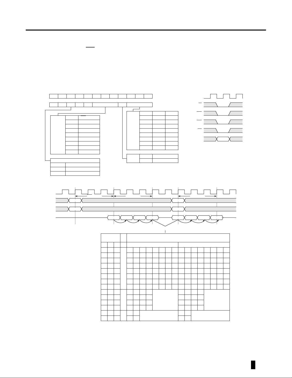
F
UNCTIONAL
A[10:0]
CLK
CKE
RAS
CAS
WE
DQML
DQMU
BA
CS
B
LOCK
Address Buffer
Clock Buffer
Signal Buffer
D
IAGRAM
Control
Mode
Register
Control Circuitry
Memory Array
Bank #0
Memory Array
Bank #1
I/O Buffer
DQ[15:0]
Figure 1. 16M (2-Bank x 524288-Word x 16-Bit) Synchronous DRAM
Signal Description
Signal
CLK Input Master Clock: All other inputs are referenced to the rising edge of CLK.
CKE Input Clock Enable: CKE controls internal clock. When CKE is low, internal clock for the following cycle is ceased. CKE
CS Input Chip Select: When CS is high, any command means No Operation.
RAS, CAS, WE Input Combination of RAS, CAS, WE defines basic commands.
A[10:0] Input A[10:0] specify the Row / Column Address in conjunction with BA. The Row Address is specified by A[10:0]. The
BA Input Bank Address: BA is not simply A[11]. BA specifies the bank to which a command is applied. BA must be set with
DQ[15:0] Input / Output Data In and Data out are referenced to the rising edge of CLK.
DQML Input Lower Din[7:0] Mask / Lower Output[7:0] Disable: When DQML is high in burst write, lower Din[7:0] for the current
DQMU Input Upper Din[15:8] Mask / Upper Output[15:8] Disable: When DQMU is high in burst write, upper Din(8-15) for the
, V
Power Supply Power Supply for the memory array and peripheral circuitry.
V
DD
SS
V
, V
DDQ
Power Supply V
SSQ
Type Description
is also used to select auto / self refresh. After self refresh mode is started, CKE becomes asynchronous input.
Self refresh is maintained as long as CKE is low.
Column Address is specified by A[7:0]. A[10] is also used to indicate precharge option. When A[10] is high at a
read / write command, an auto precharge is performed. When A[10] is high at a precharge command, both banks
are precharged.
ACT, PRE, READ, WRITE commands.
cycle is masked. When DQML is high in burst read, lower Dout[7:0] is disabled at the next but one cycle.
current cycle is masked. When DQMU is high in burst read, upper Dout[15:8] is disabled at the next but one
cycle.
DDQ
and V
are supplied to the Output Buffers only.
SSQ
2
G-LINK Technology
February 1999 (Rev.2)
F
UNCTIONAL
The GLT5160L16 provides basic functions, bank (row)
activate, burst read / write, bank (row) precharge, and
auto / self refresh. Each command is defined by control
signals of RAS
tion to 3 signals, CS
select, refresh option, and precharge option, respectively.
To know the detailed definition of commands, please see
the command truth table.
CLK
CS
RAS
CAS
WE
CKE
A[10]
D
ESCRIPTION
, CAS and WE at CLK rising edge. In addi-
, CKE and A[10] are used as chip
Chip Select: L=select, h=deselect
Command
Command
Command
Refresh option @refresh command
Precharge Option @ precharge or
read/write command
Define Basic Commands
Read (READ) [RAS = H, CAS = L, WE = H]
READ command starts burst read from the active bank
indicated by BA. First output data appears after CAS
latency. When A[10] = H at this command, the bank is
deactivated after the burst read (auto-precharge, READA).
Write (WRITE) [RAS
WRITE command starts burst write to the active bank
indicated by BA. Total data length to be written is set by
burst length. When A[10] = H at this command, the bank
is deactivated after the burst write (auto-precharge,
WRITEA).
= H, CAS =WE = L]
Precharge (PRE) [RAS = L, CAS = H, WE = L]
PRE command deactivates the active bank indicated by
BA. This command also terminates burst read / write
operation. When A[10] = H at this command, both banks
are deactivated (precharge all, PREA).
Activate (ACT) [RAS = L, CAS = WE = H]
Auto-Refresh (REFA)
ACT command activates a row in an idle bank indicated
by BA.
Command
[1]
Mnemonic CKE n-1 CKE n CS RAS CAS WE BA A[10] A[9:0]
L H L H H H X X X
Command T ruth Tab le
Deselect DESEL H X H X X X X X X
No Operation NOP H X L H H H X X X
Row Address Entry & Bank Activate ACT H X L L H H V V V
Single Bank Precharge PRE H X L L H L V L X
Precharge All Banks PREA H X L L H L V H X
Column Address Entry & Write WRITE H X L H L L V L V
Column Address Entry & Write with Auto-Precharge WRITEA H X L H L L V H V
Column Address Entry & Read READ H X L H L H V L V
Column Address Entry & Read with Auto-Precharge READA H X L H L H V H V
Auto-Refresh REFA H H L L L H X X X
Self-Refresh Entry REFS H L L L L H X X X
Self-Refresh Exit REFSX L H H X X X X X X
Burst Terminate TBST H X L H H L X X X
Mode Register Set MRS H X L L L L L L V
1. H = High Level, L = Low Level, V = Valid, X = Don't Care, n = CLK cycle number
= CAS = L, WE = CKE = H]
[RAS
REFA command starts auto-refresh cycle. Refresh
address including bank address are generated internally.
After this command, the banks are precharged automatically. Any other command should not be asserted until
t
is met.
RC
G-LINK Technology
February 1999 (Rev.2)
3
Function T ruth Tab le
Current State
[1] [2]
CS RAS CAS WE Address
[3]
Command
Action
[4]
IDLE H X X X X DESEL NOP
L H H H X NOP NOP
L H H L BA TBST ILLEGAL
L H L X BA, CA, A[10] READ / WRITE ILLEGAL
[5]
[5]
L L H H BA, RA ACT Bank Active, Latch RA
L L H L BA, A[10] PRE / PREA NOP
L L L H X REFA Auto-Refresh
L L L L Op-Code, Mode-Add MRS Mode Register Set
[6]
[7]
[7]
ROW ACTIVE H X X X X DESEL NOP
L H H H X NOP NOP
L H H L BA TBST NOP
L H L H BA, CA, A[10] READ / READA Begin Read, Latch CA, Determine Auto-
Precharge
L H L L BA, CA, A[10] WRITE / WRITEA Begin Write, Latch CA, Determine Auto-
Precharge
L L H H BA, RA ACT Bank Active / ILLEGAL
[5]
L L H L BA, A[10] PRE / PREA Precharge / Precharge All
L L L H X REFA ILLEGAL
L L L L Op-Code, Mode-Add MRS ILLEGAL
READ H X X X X DESEL NOP (Continue Burst to END)
L H H H X NOP NOP (Continue Burst to END)
L H H L BA TBST Terminate Burst
L H L H BA, CA, A[10] READ / READA Terminate Burst, Latch CA, Begin New
Read, Determine Auto-Precharge
L H L L BA, CA, A[10] WRITE / WRITEA Terminate Burst, Latch CA, Begin Write,
Determine Auto-Precharge
L L H H BA, RA ACT Bank Active / ILLEGAL
[5]
L L H L BA, A[10] PRE / PREA Terminate Burst, Precharge
L L L H X REFA ILLEGAL
L L L L Op-Code, Mode-Add MRS ILLEGAL
WRITE H X X X X DESEL NOP (Continue Burst to END)
L H H H X NOP NOP (Continue Burst to END)
L H H L BA TBST Terminate Burst
L H L H BA, CA, A[10] READ / READA Terminate Burst, Latch CA, Begin Read,
Determine Auto-Precharge
L H L L BA, CA, A[10] WRITE / WRITEA Terminate Burst, Latch CA, Begin Write,
Determine Auto-Precharge
L L H H BA, RA ACT Bank Active / ILLEGAL
[5]
L L H L BA, A[10] PRE / PREA Terminate Burst, Precharge
L L L H X REFA ILLEGAL
L L L L Op-Code, Mode-Add MRS ILLEGAL
[8]
[8]
[8]
[8]
4
G-LINK Technology
February 1999 (Rev.2)
Function T ruth Tab le
Current State
READ with AUTO
PRECHARGE
[1] [2]
(Continued)
CS RAS CAS WE Address
[3]
Command
Action
H X X X X DESEL NOP (Continue Burst to END)
L H H H X NOP NOP (Continue Burst to END)
L H H L X TBST ILLEGAL
L H L H BA, CA, A[10] READ / READA ILLEGAL
L H L L BA, CA, A[10] WRITE / WRITEA ILLEGAL
L L H H BA, RA ACT Bank Active / ILLEGAL
L L H L BA, A[10] PRE / PREA ILLEGAL
[5]
L L L H X REFA ILLEGAL
L L L L Op-Code, Mode-Add MRS ILLEGAL
WRITE with AUTO
PRECHARGE
H X X X X DESEL NOP (Continue Burst to END)
L H H H X NOP NOP (Continue Burst to END)
L H H L X TBST ILLEGAL
L H L H BA, CA, A[10] READ / READA ILLEGAL
L H L L BA, CA, A[10] WRITE / WRITEA ILLEGAL
L L H H BA, RA ACT Bank Active / ILLEGAL
L L H L BA, A[10] PRE / PREA ILLEGAL
[5]
L L L H X REFA ILLEGAL
L L L L Op-Code, Mode-Add MRS ILLEGAL
PRE -CHARGING H X X X X DESEL NOP (Idle after t
L H H H X NOP NOP (Idle after t
L H H L X TBST ILLEGAL
L H L X BA, CA, A[10] READ / WRITE ILLEGAL
L L H H BA, RA ACT ILLEGAL
L L H L BA, A[10] PRE / PREA NOP
[5]
[5]
[5]
[6]
(Idle after t
)
RP
)
RP
RP
L L L H X REFA ILLEGAL
L L L L Op-Code, Mode-Add MRS ILLEGAL
ROW ACTIVATING H X X X X DESEL NOP (Row Active after t
L H H H X NOP NOP (Row Active after t
L H H L X TBST ILLEGAL
L H L X BA, CA, A[10] READ / WRITE ILLEGAL
L L H H BA, RA ACT ILLEGAL
L L H L BA, A[10] PRE / PREA ILLEGAL
[5]
[5]
[5]
[5]
L L L H X REFA ILLEGAL
L L L L Op-Code, Mode-Add MRS ILLEGAL
WRITE RECOVERING H X X X X DESEL NOP
L H H H X NOP NOP
L H H L X TBST ILLEGAL
L H L X BA, CA, A[10] READ / WRITE ILLEGAL
L L H H BA, RA ACT ILLEGAL
L L H L BA, A[10] PRE / PREA ILLEGAL
[5]
[5]
[5]
[5]
L L L H X REFA ILLEGAL
L L L L Op-Code, Mode-Add MRS ILLEGAL
[4]
[5]
[5]
)
)
RCD
)
RCD
G-LINK Technology
February 1999 (Rev.2)
5
Function T ruth Tab le
Current State
[1] [2]
(Continued)
CS RAS CAS WE Address
[3]
Command
REFRESHING H X X X X DESEL NOP (Idle after t
L H H H X NOP NOP (Idle after t
L H H L X TBST ILLEGAL
L H L X BA, CA, A[10] READ / WRITE ILLEGAL
L L H H BA, RA ACT ILLEGAL
L L H L BA, A[10] PRE / PREA ILLEGAL
L L L H X REFA ILLEGAL
L L L L Op-Code, Mode-Add MRS ILLEGAL
MODE REGISTER
SETTING
H X X X X DESEL NOP (Idle after t
L H H H X NOP NOP (Idle after t
L H H L X TBST ILLEGAL
L H L X BA, CA, A[10] READ / WRITE ILLEGAL
L L H H BA, RA ACT ILLEGAL
L L H L BA, A[10] PRE / PREA ILLEGAL
L L L H X REFA ILLEGAL
L L L L Op-Code, Mode-Add MRS ILLEGAL
1. H = High Level, L= Low Level, X = Don't Care.
2. All entries assume that CKE was High during the preceding clock cycle and the current clock cycle.
3. BA = Bank Address, RA = Row Address, CA = Column Address, NOP = No OPeration.
4. ILLEGAL = Device operation and/or data-integrity are not guaranteed.
5. ILLEGAL to bank in specified state; function may be legal in the bank indicated by BA, depending on the state of that bank.
6. NOP to bank precharging or in idle state. May precharge bank indicated by BA.
7. ILLEGAL if any bank is not idle.
8. Must satisfy bus contention, bus turn around, write recovery requirements.
Action
)
RC
)
RC
)
RSC
)
RSC
[4]
6
G-LINK Technology
February 1999 (Rev.2)
Function T ruth Tab le for CKE
Current State
SELF-REFRESH
[2]
H X X X X X X INVALID
CKE n-1 CKE n CS RAS CAS WE Add Action
[1]
L H H X X X X Exit Self-Refresh (Idle after t
L H L H H H X Exit Self-Refresh (Idle after t
L H L H H L X ILLEGAL
L H L H L X X ILLEGAL
L H L L X X X ILLEGAL
L L X X X X X NOP (Maintain Self-Refresh)
POWER DOWN H X X X X X X INVALID
L H X X X X X Exit Power Down to Idle
L L X X X X X NOP (Maintain Self-Refresh)
ALL BANKS IDLE
[3]
H H X X X X X Refer to Function Truth Table
H L L L L H X Enter Self-Refresh
H L H X X X X Enter Power Down
H L L H H H X Enter Power Down
H L L H H L X ILLEGAL
H L L H L X X ILLEGAL
H L L L X X X ILLEGAL
L X X X X X X Refer to Current State = Power Down
ANY STATE other than
listed above
H H X X X X X Refer to Function Truth Table
H L X X X X X Begin CLK Suspend at Next Cycle
L H X X X X X Exit CLK Suspend at Next Cycle
L L X X X X X Maintain CLK Suspend
1. H = High Level, L= Low Level, X = Don't Care.
2. CKE Low to High transition will re-enable CLK and other inputs asynchronously. A minimum setup time must be satisfied before any command other than EXIT.
3. Power-Down and Self-Refresh can be entered only from the All Banks Idle State.
4. Must be legal command.
)
RC
)
RC
[4]
[4]
G-LINK Technology
February 1999 (Rev.2)
7
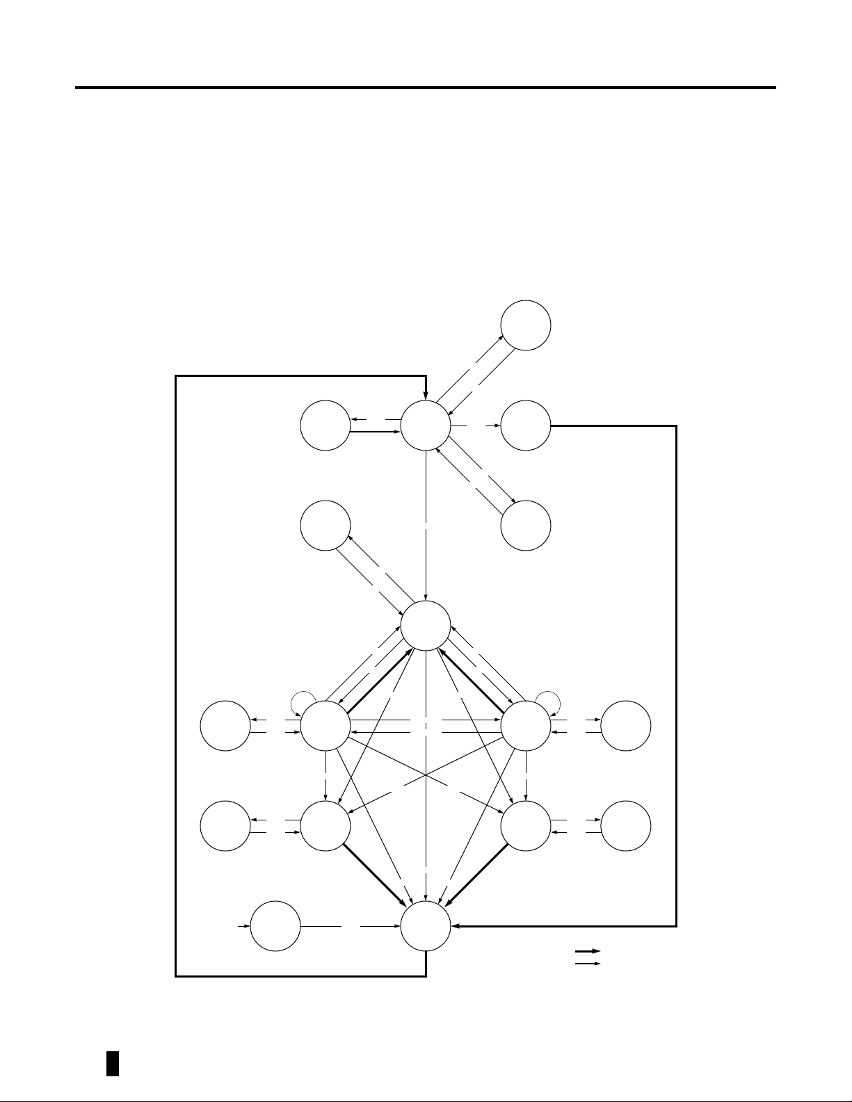
Power On Sequence
Before starting normal operation, the following power on
sequence is necessary to prevent damage or malfunction.
1. Apply power and start clock. Attempt to maintain
CKE high, DQMU / DQML high and NOP condition
at the inputs.
2. Maintain stable power, stable clock, and NOP input
conditions for a minimum of 200 µ s.
MODE
REGISTER
SET
CLK
SUSPEND
MRS
3. Issue precharge commands for all banks. (PRE or
PREA)
4. After all banks become idle state (after t
), issue 2
RP
or more auto-refresh commands.
5. Issue a mode register set command to initialize the
mode register.
After this sequence, the SDRAM is idle state and ready for
normal operation.
SELF
REFRESH
REFS
REFSX
CKEL
AUTO
REFRESH
POWER
DOWN
IDLE
ACT
REFA
CKEH
WRITE
SUSPEND
WRITE A
SUSPEND
POWER
APPLIED
CKEL
CKEH
CKEH
CKEL
CKEH
ROW ACTIVE
TBST TBST
WRITE READ
WRITE A READE A
WRITE READ
WRITE A READE A
WRITE A READ A
PRE
READ
WRITE
WRITE A READE A
PRE
PRE
PRE
PRECHARGEPOWER ON
CKEL
CKEH
CKELCKEL
CKEH
READ
SUSPEND
READ A
SUSPEND
Automatic Sequence
Command Sequence
Figure 2. Simplified State Diagram
8
G-LINK Technology
February 1999 (Rev.2)
Mode Register
Burst Length, Burst Type and CAS Latency can be programmed by setting the mode register (MRS). The mode
register stores these data until the next MRS command,
which may be issued when both banks are in idle state.
After t
new command.
from a MRS command, the SDRAM is ready for
RSC
BA A10 A9 A8 A7 A6 A5 A4 A3 A2 A1 A0
0 0 WBL 0 Ø LTMODE BT BL
CL
CAS LATENCY
000
001
0
LATENCY
MODE
A9
CLK
Command READ
Address
DQ
1
0
1
1
0
1
0
1
1
1
1
Write Burst Length (WBL)
Length
ø
= BL specified
1
Single bit (BL = 1)
R
R
0
2
1
3
0
R
1
R
0
R
1
R
CAS Latency Burst Length Burst Length
Y
Q0 Q1 Q3
BL
BT = 0 BT = 1
000
001
0
BURST
0
LENGTH
1
1
1
1
0BURST
TYPE
1
Q2 D0 D1 D3D2
1
1
0
0
1
1
0
1
0
1
0
1
Full Page
1
2
4
8
R
R
R
SEQUENTIAL
INTERLEAVED
Burst Type
1
2
4
8
R
R
R
R
WRITE
Y
CLK
CS
RAS
CAS
WE
BA, A[10:0]
Initial
Address BL Column Addressing
A2 A1 A0 Sequential Interleaved
00080123456701234567
001 1234567010325476
010 2345670123016745
011 3456701232107654
100 4567012345670123
101 5670123454761032
110 6701234567452301
111 7012345676543210
–0040123 0123
–01 1230 1032
–10 2301 2301
–11 3012 3210
––0201 01
––1 10 10
G-LINK Technology
February 1999 (Rev.2)
9
O
PERATIONAL
D
ESCRIPTION
Bank Activate
The SDRAM has two independent banks. Each bank is
activated by the ACT command with the bank address
(BA). A row is indicated by the row address A[10:0] The
minimum activation interval between one bank and the
other bank is t
Command
CLK
A[9:0]
A[10]
RRD
BA
DQ
.
ACT ACT READ PRE ACT
t
RRD
Xa
Xa
0
Xb Ya
Xb 0
01 1
Figure 3. Bank Activation and Precharge All (BL=4, CL=3)
Precharge
The PRE command deactivates the bank indicated by BA.
When both banks are active, the precharge all command
(PREA, PRE + A[10] = H) is available to deactivate them at
the same time. After t
mand can be issued.
t
RAS
1
Qa2Qa1Qa0 Qa3
from the precharge, an ACT com-
RP
t
RP
Precharge All
Xb
Xb
10
G-LINK Technology
February 1999 (Rev.2)
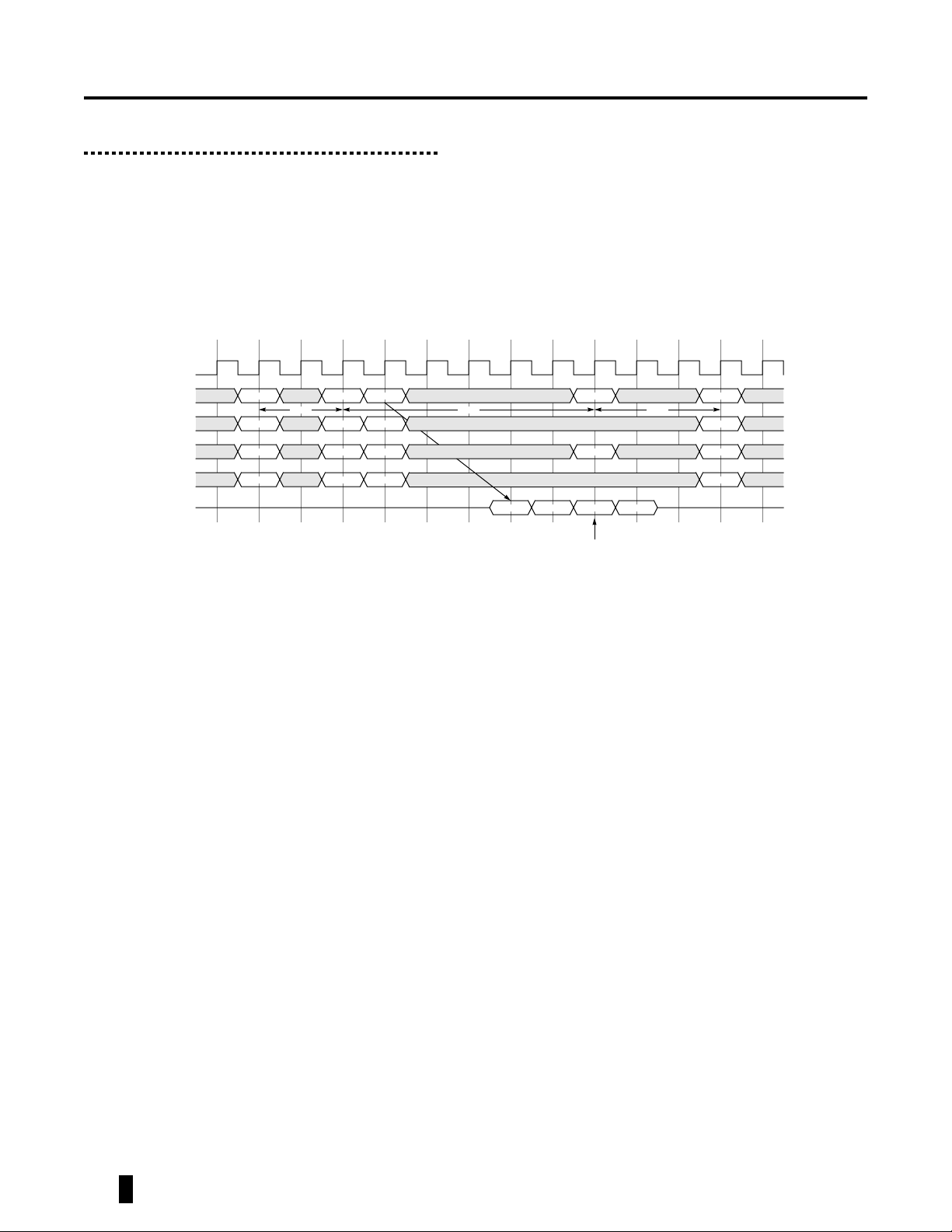
Read
After t
can be issued. 1st output data is available after the CAS
Latency from the READ, followed by (BL-1) consecutive
data when the Burst Length is BL. The start address is
specified by A[7:0], and the address sequence of burst
data is defined by the Burst Type. A READ command may
be applied to any active bank, so the row precharge time
from the bank activation, a READ command
RCD
CLK
(t
) can be hidden behind continuous output data (in
RP
case of BL ≥ 4) by interleaving the dual banks. When A[10]
is high at a READ command, the auto-precharge (READA)
is performed. Any command (READ, WRITE, PRE, ACT) to
the same bank is inhibited till the internal precharge is
complete. The internal precharge start timing depends on
Burst Length. The next ACT command can be issued after
t
from the internal precharge timing.
RP
Command
A[9:0]
A[10]
CLK
Command
A[9:0]
A[10]
ACT READ ACT PRE
Xa Ya Xb Yb
Xa 0 Xb 00
BA
DQ
0 0 1 01
t
RCD
CAS Latency
READ
Burst Length
Qa2Qa1Qa0 Qa3
Qb0 Qb1 Qb2
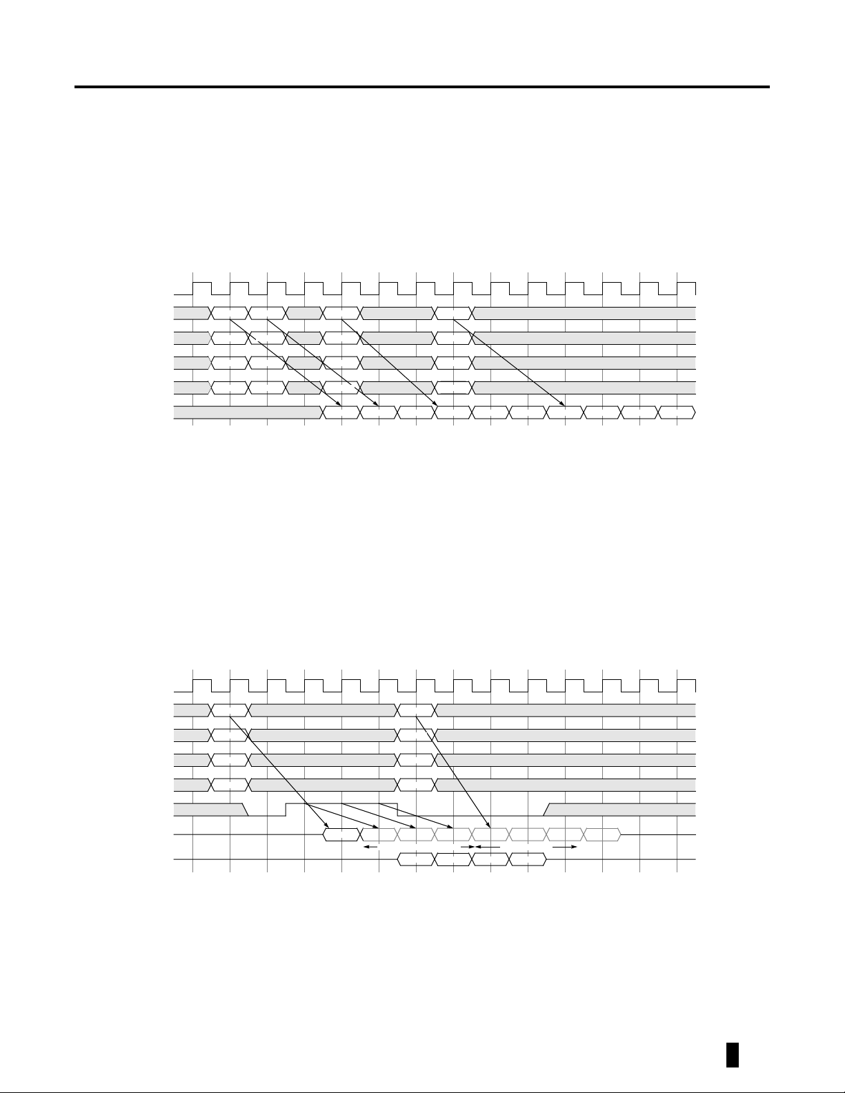
Figure 4. Dual Bank Interleaving READ (BL=4, CL=3)
ACT READ A ACT
Xa Y Xa
Xa 1 Xa
BA
DQ
0 0 0
t
RCD
Internal Precharge begins
t
RP
Qa2Qa1Qa0 Qa3
Figure 5. READ with Auto-Precharge (BL=4, CL=3)
CLK
Command
CL=3 DQ
CL=2 DQ
ACT READ A
Figure 6. READ Auto-Precharge Timing (BL=4)
Qa2Qa1Qa0 Qa3
Qa2Qa1Qa0 Qa3
Internal Precharge Start Timing
G-LINK Technology
February 1999 (Rev.2)
11
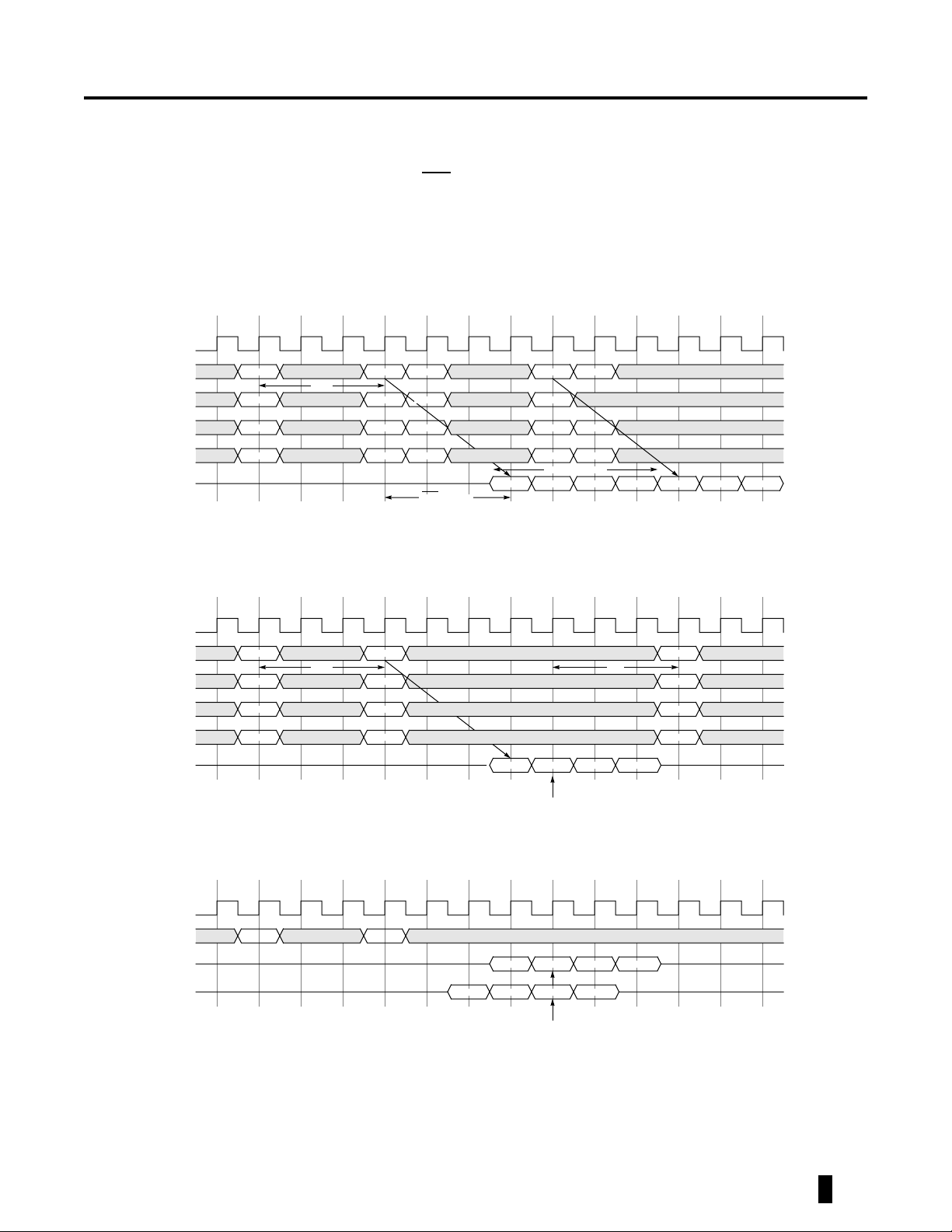
Write
After t
can be issued. 1st input data is set at the same cycle as
the WRITE. Following (BL-1) data are written into the
RAM, when the Burst Length is BL. The start address is
specified by A[7:0], and the address sequence of burst
data is defined by the Burst Type. A WRITE command
may be applied to any active bank, so the row precharge
time (t
from the bank activation, a WRITE command
RCD
) can be hidden behind continuous input data (in
RP
CLK
Command
A[9:0]
A[10]
BA
DQ
ACT WRITE ACT PREWRITE
Xa Y Xb Y
Xa 0 Xb 00
0 0 1 01
t
RCD
Figure 7. Dual Bank Interleaving WRITE (BL=4)
Burst Length
case of BL ≥ 4) by interleaving the dual banks. From the
last input data to the PRE command, the write recovery
time (t
) is required. When A[10] is high at a WRITE
RDL
command, the auto-precharge (WRITEA) is performed.
Any command (READ, WRITE, PRE, ACT) to the same
bank is inhibited till the internal precharge is complete.
The internal precharge begins at t
after the last input
RDL
data cycle. The next ACT command can be issued after
t
from the internal precharge timing.
RP
t
RCD
t
(1 CLK)
RDL
Da2Da1Da0 Da3
Db1Db0 Db3Db2
CLK
Command
A[9:0]
A[10]
ACT WRITE ACT
Xa Y Xa
Xa 1 Xa
BA
DQ
0 0 0
t
RCD
t
RDL
Da2Da1Da0 Da3
Internal Precharge Begins
t
RP
Figure 8. WRITE with Auto-Precharge (BL=4)
12 G-LINK Technology
February 1999 (Rev.2)
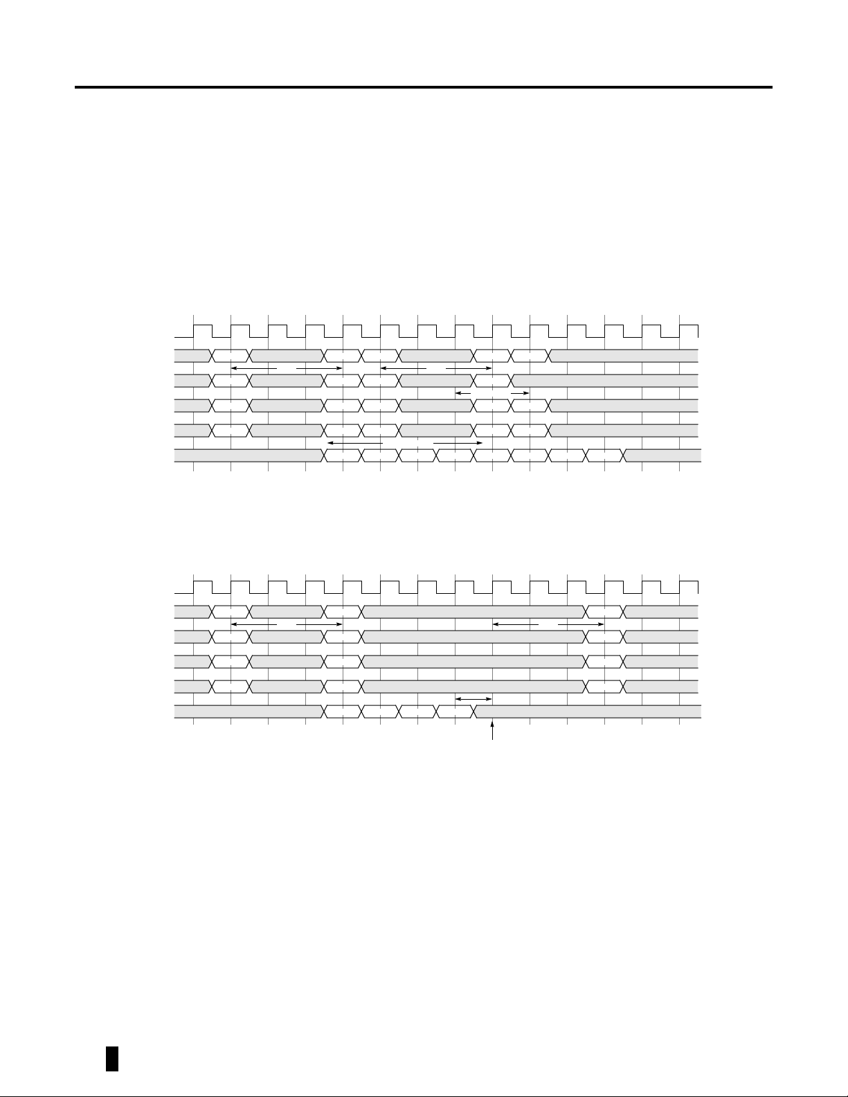
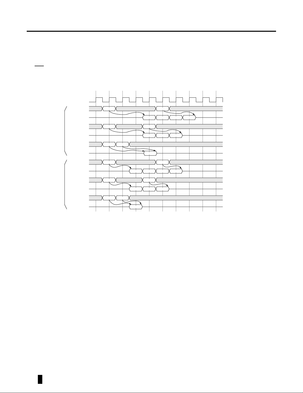
Burst Interruption
[Read Interrupted by Read]
The burst read operation can be interrupted by a new
read of the same or the other bank. GLT5160L16 allows
random column access. READ to READ interval is 1 CLK
minimum.
CLK
Command
A[9:0]
A[10]
BA
DQ
READ READ READ
READ
Yi Yk YlYj
0 0 00
0 10
Figure 9. READ Interrupted by READ (BL=4, CL=3)
[Read Interrupted by Write]
Burst read operation can be interrupted by write of the
same or the other bank. Random column access is
allowed. In this case, the DQ should be controlled adequately by using the DQMU / DQML to prevent the bus
contention. The output is disabled automatically 2 cycles
after WRITE assertion.
CLK
Command
READ
Qj1Qj0Qi0 Qk0
WRITE
0
Qk2Qk1 Ql1Ql0
Internal Precharge Start Timing
Ql2 Ql3
A[9:0]
A[10]
BA
DQMU, DQML
Q
D Dj0
Yi Yj
0 0
0 0
Figure 10. READ Interrupted by WRITE (BL=4, CL=3)
Qi0
DQM U/ DQML control Write control
Dj1
Dj3Dj2
13G-LINK Technology
February 1999 (Rev.2)
[Read Interrupted by Precharge]
Burst read operation can be interrupted by precharge of
the same bank. READ to PRE interval is minimum 1 CLK.
A PRE command disables the data output, depending on
the CAS
when the data-out is terminated.
Latency. The figure below shows examples,
CLK
CL=3
CL=2
Command
Command
Command
Command
Command
Command
READ PRE
DQ
READ PRE
DQ
READ PRE
DQ
READ PRE
DQ
READ PRE
DQ
READ PRE
DQ
Q 0 Q 1 Q 2 Q 3
Q 0 Q 1 Q 2
Q 0
Q 0 Q 1 Q 2 Q 3
Q 0 Q 1 Q 2
Q 0
Figure 11. READ Interrupted by Precharge (BL=4)
14 G-LINK Technology
February 1999 (Rev.2)
 Loading...