

Datasheet GLT41016-35J4, GLT41016-30TC, GLT41016-30J4, GLT41016-45J4, GLT41016-40J4 Datasheet (G-LINK)
G-LINK
CAS
RAS
CAS
RAS
CAS
RAS
CAS
64K X 16 CMOS DYNAMIC RAM WITH EXTENDED DATA OUTPUT
Features : Description :
GLT41016
Dec 1998 (Rev 2.1)
∗ 65,536 words by 16 bits organization.
∗ Fast access time and cycle time.
∗ Dual
Input.
∗ Low power dissipation.
∗ Read-Modify-Write,
-Before-
Refresh and Test Mode Capability.
Refresh, Hidden
-Only Refresh,
∗ 256 refresh cycles per 4ms.
∗ Available in 40-pin 400 mil SOJ and 40/44
pin TSOP (II).
∗ Single 5.0V±10% Power Supply.
∗ All inputs and Outputs are TTL
compatible.
∗ Extended Data-Out(EDO) Page Mode
operation.
The GLT41016 is a 65,536 x 16 bit highperformance CMOS dynamic random access
memory. The GLT41016 offers Fast Page
mode with Extended Data Output, and has
both BYTE WRITE and WORD WRITE
access cycles via two
pins. The
GLT41016 accepts 256-cycle refresh in 4ms
interval.
All inputs are TTL compatible. EDO
Page Mode operation allows random access
up to 256 x 16 bits, within a page, with cycle
times as short as 12ns.
The GLT41016 is best suited for
graphics, and DSP applications requiring
high performance memories.
HIGH PERFORMANCE 30 35 40 45
Max.
Access Time, (t
RAC
)
30 ns 35 ns 40 ns 45 ns
Max. Column Address Access Time, (tAA) 15 ns 18 ns 20 ns 22 ns
Min. Extended Data Out Page Mode Cycle Time, (tPC) 12 ns 13 ns 15 ns 18 ns
Min. Read/Write Cycle Time, (tRC) 65 ns 70 ns 75 ns 80 ns
Max.
G-Link Technology Corporation
2701Northwestern Parkway
Santa Clara, CA 95051, U.S.A.
Access Time (t
CAC
)
10 ns 11 ns 12 ns 12 ns
G-Link Technology Corporation, Taiwan
2F, No.12, R&D Rd. II, Science-Based Industrial Park,
Hsin Chu, Taiwan, R.O.C.
- 1 -
G-LINK
RAS
UCAS
LCAS
WE
OE
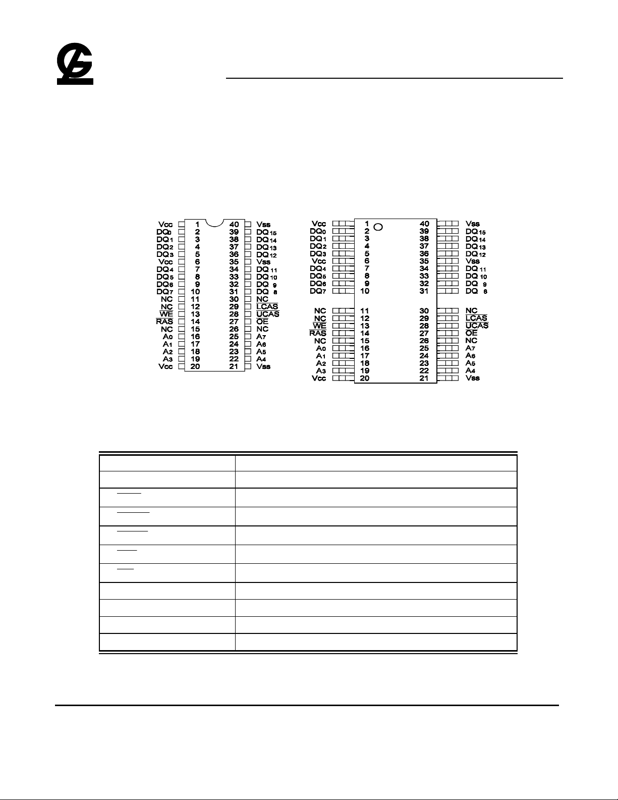
Pin Configuration :
GLT41016
64K X 16 CMOS DYNAMIC RAM WITH EXTENDED DATA OUTPUT
Dec 1998 (Rev 2.1)
Pin Descriptions:
GLT41016
SOJ Top View
TSOP(Type II)
Top View
Name Function
A0 - A
DQ0 - DQ
V
V
7
15
CC
SS
NC No Connection
G-Link Technology Corporation
2701Northwestern Parkway
Santa Clara, CA 95051, U.S.A.
Address Inputs
Row Address Strobe
Column Address Strobe/Upper Byte Control
Column Address Strobe/Lower Byte Control
Write Enable
Output Enable
Data Inputs / Outputs
+5V Power Supply
Ground
G-Link Technology Corporation, Taiwan
2F, No.12, R&D Rd. II, Science-Based Industrial Park,
Hsin Chu, Taiwan, R.O.C.
- 2 -
G-LINK
RAS
LCAS
UCAS
WE,OE
CAS
UCAS
LCAS
CAS
RAS
RAS
64K X 16 CMOS DYNAMIC RAM WITH EXTENDED DATA OUTPUT
Absolute Maximum Ratings* Capacitance*
TA=25°C, VCC=5V±10%, VSS=0V
GLT41016
Dec 1998 (Rev 2.1)
Operating Temperature, TA (ambient)
Symbol
.......................................-0°C to +70°C
C
Storage Temperature(plastic)....-55°C to +150°C
Voltage Relative to VSS...............-1.0V to + 7.0V
IN1
C
IN2
Short Circuit Output Current......................50mA
C
Power Dissipation......................................1.0W
*Note: Operation above Absolute Maximum Ratings
can adversely affect device reliability.
OUT
*Note: Capacitance is sampled and not 100% tested
Electrical Specifications
l
l All voltages are referenced to GND.
l After power up, wait more than 100µs and then, execute eight
means
and
.
refresh cycles as dummy cycles to initialize internal circuit.
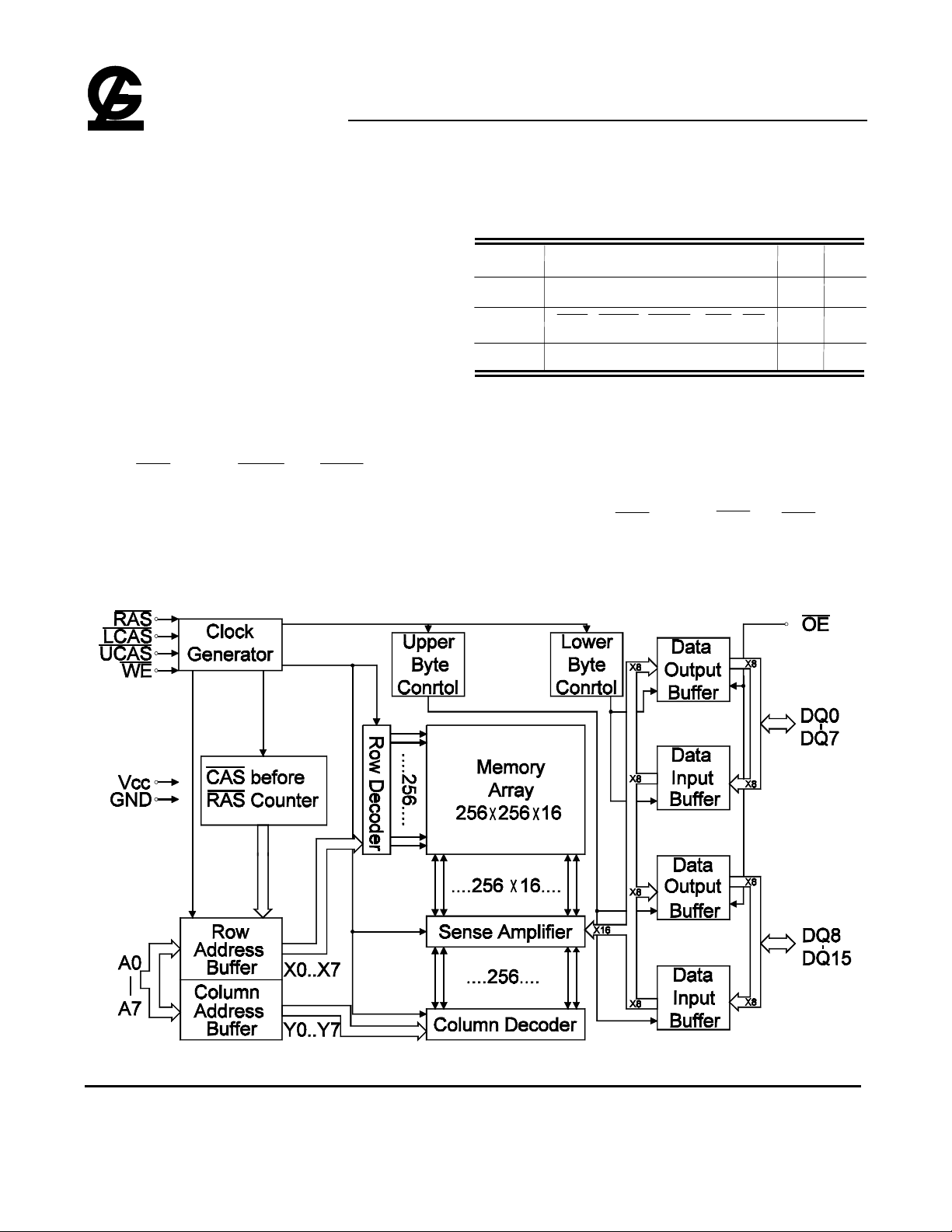
Block Diagram :
Parameter
Address Input
,
Data Input/ Output
,
-before-
Max.
,
or
Unit
5
pF
7
pF
7
pF
-only
G-Link Technology Corporation
2701Northwestern Parkway
Santa Clara, CA 95051, U.S.A.
G-Link Technology Corporation, Taiwan
2F, No.12, R&D Rd. II, Science-Based Industrial Park,
Hsin Chu, Taiwan, R.O.C.
- 3 -
G-LINK
CAS
CAS
CAS
CAS
CAS
CAS
RAS
64K X 16 CMOS DYNAMIC RAM WITH EXTENDED DATA OUTPUT
GLT41016
Dec 1998 (Rev 2.1)
Extended Data Output (EDO) Page Mode
The EDO page mode is a kind of page mode with enhanced features. The two major features
of the EDO page mode are as follows.
1. Data output time is extended.
In the EDO page mode, the output data is held to the next
cycle‘s falling edge,
instead of the rising edge. For this reason, valid data output time in the EDO page mode is
extended compared with the fast page mode (=data extend function). In the fast page mode,
the data output time becomes shorter as the
cycle time becomes shorter. Therefore, in
the EDO page mode, the timing margin in read cycle is larger than of the fast page mode
even if the
2. The
In the EDO page mode, due to the data extend function, the
cycle time becomes shorter.
cycle time in the EDO page mode is shorter than that in the fast page mode.
cycle time can be
shorter than in the fast page mode if the timing margin is the same.
Taking a device whose t
is 60ns as an example, the
RAC
cycle time in the EDO page
mode is 25ns while that in the fast page mode is 40ns.
In the EDO page mode, read (data out) and write (data in) cycles can be executed
repeatedly during one
cycle. The EDO page mode allows both read and write
operations during one cycle, but the performance is equivalent to that of the fast page mode
in that case.
G-Link Technology Corporation
2701Northwestern Parkway
Santa Clara, CA 95051, U.S.A.
G-Link Technology Corporation, Taiwan
2F, No.12, R&D Rd. II, Science-Based Industrial Park,
Hsin Chu, Taiwan, R.O.C.
- 4 -
G-LINK
RAS
CASL
CASH
WE
OE
RAS
UCAS
LCAS
UCAS
LCAS
UCAS
LCAS
Truth Table: GLT41016
GLT41016
64K X 16 CMOS DYNAMIC RAM WITH EXTENDED DATA OUTPUT
Dec 1998 (Rev 2.1)
Function
Standby H
Read: Word L L L H L ROW/COL Data Out
Read: Lower Byte L L H H L ROW/COL Lower Byte,Data-
Read: Upper Byte L H L H L ROW/COL Lower Byte,High-Z
Write: Word(Early Write) L L L L X ROW/COL Data-In
Write: Lower Byte (Early) L L H L X ROW/COL Lower Byte,Data-In
Write: Upper Byte (Early) L H L L X ROW/COL Lower Byte,High-Z
Read Write L L L
EDO-PageMode Read
EDO-PageMode Write
1st Cycle
2nd Cycle
1st Cycle
2nd Cycle
L
L
L
L
H→X H→X
H→L
H→L
H→L
H→L
H→L
H→L
H→L
H→L
X X High-Z
H→L L→H
H
H
L
L
ADDRESS DQs Notes
Out
Upper Byte,High-Z
Upper Byte,DataOut
Upper Byte,High-Z
Upper Byte,Data-In
ROW/COL Data-Out,Data-In 1,2
L
L
X
X
ROW/COL
COL
ROW/COL
COL
Data-Out
Data-Out
Data-In
Data-In
1
1
2
2
EDO-PageMode ReadWrite
Hidden
Refresh
-Only Refresh
CBR Refresh
1st Cycle
2nd Cycle
Read
Write
L
L
L→H→L
L→H→L
L H H X X ROW High-Z
H→L
H→L
H→L
H→L
H→L
L
L
L L X X High-Z 4
H→L
H→L
L
L
H
L
Notes:
1. These READ cycles may also be BYTE READ cycles (either
2. These WRITE cycles may also be BYTE READ cycles (either
3. EARLY WRITE only.
4. At least one of the two CAS signals must be active (
G-Link Technology Corporation
2701Northwestern Parkway
Santa Clara, CA 95051, U.S.A.
- 5 -
L→H
L→H
or
ROW/COL
COL
L
ROW/COL
X
ROW/COL
or
or
).
G-Link Technology Corporation, Taiwan
2F, No.12, R&D Rd. II, Science-Based Industrial Park,
Hsin Chu, Taiwan, R.O.C.
Data-Out,Data-In
Data-Out,Data-In
Data-Out
Data-In
active).
active).
1,2
1,2
1
2,3
G-LINK
CC1
CC2
RAS
UCAS
LCAS
CC3
RAS
RAS
UCAS
LCAS
CC4
RAS
UCAS
LCAS
CC5
RAS
RAS
UCAS
LCAS
CC6
RAS
UCAS
LCAS
64K X 16 CMOS DYNAMIC RAM WITH EXTENDED DATA OUTPUT
DC and Operating Characteristics (1-2)
TA = 0°C to 70°C, VCC=5V±10%, VSS=0V, unless otherwise specified.
GLT41016
Dec 1998 (Rev 2.1)
Sym
Parameter Test Conditions Access
.
I
Input Leakage Current
LI
(any input pin)
I
Output Leakage Current
LO
(for High-Z State)
I
Operating Current,
Random READ/WRITE tRC = tRC (min.)
I
Standby Current,(TTL)
I
Refresh Current,
-Only
I
Operating Current,
EDO Page Mode
I
Refresh Current,
CAS Before
I
Standby Current, (CMOS)
0V ≤ V
≤ 5.5V
IN
(All other pins not under
test=0V)
0V ≤ V
out
≤ 5.5V
Output is disabled (Hiz)
,
V
other inputs ≥V
IH
cycling,
at V
,
at
SS
,
IH
tRC = tRC (min.)
at VIL,
,
cycling: t
,
address
= tPC(min.)
PC
,
address cycling:
t
= tRC (min.)
RC
≥VCC-0.2V,
≥VCC-0.2V,
t
RAC
t
RAC
t
RAC
t
RAC
t
RAC
t
RAC
t
RAC
t
RAC
t
RAC
t
RAC
t
RAC
t
RAC
t
RAC
t
RAC
t
RAC
t
RAC
Time
= 30ns
= 35ns
= 40ns
= 45ns
= 30ns
= 35ns
= 40ns
= 45ns
= 30ns
= 35ns
= 40ns
= 45ns
= 30ns
= 35ns
= 40ns
= 45ns
Min. Typ Max. Unit Notes
-10 +10
-10 +10
180
170
160
150
4 mA
180
170
160
150
180
170
160
150
180
170
160
150
2 mA
µA
µA
mA 1,2
mA 2
mA 1,2
mA 1
≥VCC-0.2V,
All other inputs V
SS
VILInput Low Voltage -1 +0.8 V 3
VIHInput High Voltage 2.4 VCC+1 V 3
VOLOutput Low Voltage IOL = 4.2mA 0.4 V
VOHOutput High Voltage IOH = -5mA 2.4 V
Notes:
1. ICC is dependent on output loading when the device output is selected. Specified ICC(max.) is measured with the output
open.
2. ICC is dependent upon the number of address transitions specified ICC(max.) is measured with a maximum of one
transition per address cycle in random Read/Write and EDO Fast Page Mode.
3. Specified VIL(min.) is steady state operation. During transitions VIL(min.) may undershoot to -1.0V for a period not to
exceed 20ns. All AC parameters are measured with VIL(min.)≥VSS and VIH(max.)≤VCC.
G-Link Technology Corporation
2701Northwestern Parkway
Santa Clara, CA 95051, U.S.A.
G-Link Technology Corporation, Taiwan
2F, No.12, R&D Rd. II, Science-Based Industrial Park,
Hsin Chu, Taiwan, R.O.C.
- 6 -
G-LINK
CAS
RAS
RAS
RAS
RAS
RAS
CAS
CAS
CAS
RAS
RAS
OE
CAS
CAS
RAS
RAS
CAS
RAS
RAS
RAS
CAS
RAS
64K X 16 CMOS DYNAMIC RAM WITH EXTENDED DATA OUTPUT
AC Characteristics
TA = 0°C to 70°C , VCC = 5 V ± 10%, VIH/VIL = 2.4/0.8 V, VOH/VOL = 2.0/0.8V
GLT41016
Dec 1998 (Rev 2.1)
An initial pause of 100 µs and 8
-before-
or
-only refresh cycles are required after power-up.
30 35 40 45
Parameter Symbol Min. Max. Min. Max. Min. Max. Min. Max. Unit Notes
Read or Write Cycle Time
Read Modify Write Cycle Time
Precharge Time
Pulse Width
Access Time from
Access Time from
Access Time from Column Address
to Output Low-Z
to Output High-Z
Hold Time
Hold Time Referenced to
Hold Time
Pulse Width
to CAS Delay Time
to Column Address Delay Time
to
Precharge Time
Row Address Set-Up Time
Row Address Hold Time
Column Address Set-Up Time
Column Address Hold Time
Column Address to
Lead Time
Column Address Hold Time Referenced to
t
RC
t
RWC
t
RP
t
RAS
t
RAC
t
CAC
t
AA
t
CLZ
t
CEZ
t
RSH
t
ROH
t
CSH
t
CAS
t
RCD
t
RAD
t
CRP
t
ASR
t
RAH
t
ASC
t
CAH
t
RAL
t
AR
65 70 75 80 ns
90 95 100 103 ns
25 25 25 30 ns
30 100k 35 100k 40 100k 45 100k ns
30 35 40 45 ns 1,2,3
10 11 12 12 ns 1,5,10
15 18 20 22 ns 1,5,6
0 0 0 0 ns
3 8 3 8 3 8 3 8 ns
10 12 12 13 ns
7 8 8 9 ns
25 30 34 40 ns
6 10k 6 10k 6 10K 7 10K ns
13 20 17 24 18 28 18 33 ns
10 15 12 17 13 20 13 23 ns 7
5 5 5 5 ns
0 0 0 0 ns
6 7 8 8 ns
0 0 0 0 ns
6 6 6 6 ns
15 18 20 23 ns
26 30 34 39 ns
Read Command Set-Up Time
Read Command Hold Time Referenced to
Read Command Hold Time Referenced to
Write Command Set-Up Time
Write Command Hold Time
Write Command Pulse Width
G-Link Technology Corporation
2701Northwestern Parkway
Santa Clara, CA 95051, U.S.A.
t
RCS
t
RCH
t
RRH
t
WCS
t
WCH
t
WP
0 0 0 0 ns
0 0 0 0 ns 4
0 0 0 0 ns 4
0 0 0 0 ns 8,9
6 6 6 6 ns
6 6 6 6 ns
G-Link Technology Corporation, Taiwan
2F, No.12, R&D Rd. II, Science-Based Industrial Park,
Hsin Chu, Taiwan, R.O.C.
- 7 -

G-LINK
RAS
CAS
RAS
RAS
CAS
RAS
CAS
CAS
CAS
RAS
OE
OE
OE
OE
CAS
RAS
WE
OE
CAS
CAS
OE
OE
CAS
CAS
RAS
CAS
CAS
RAS
GLT41016
64K X 16 CMOS DYNAMIC RAM WITH EXTENDED DATA OUTPUT
Dec 1998 (Rev 2.1)
AC Characteristics
30 35 40 45
Parameter Symbol Min. Max. Min. Max. Min. Max. Min. Max. Unit Notes
Write Command to
Write Command to
Lead Time
Lead Time
Data Set-Up Time
Data Hold Time
Data Hold Time Referenced to
to WE Delay Time
to WE Delay Time
Column Address to WE Delay Time
to
Access Time from
Precharge Time
Precharge
EDO Page Mode Cycle Time
EDO Page Mode Read-Modify-Write Cycle Time
Precharge Time (EDO Page Mode)
Pulse Width (EDO Page Mode Only)
Access Time from
to Data Delay Time
to Output High-Z
Command Hold Time
Data Output Hold after
low
to Output High-Z
to Output High-Z
to
Hold Time
Hold Time to
Precharge Time
Set-Up Time for
Hold Time for
-before-
-before-
Cycle
Cycle
Transition Time
Refresh Period
t
RWL
t
CWL
t
DS
t
DH
t
DHR
t
RWD
t
CWD
t
AWD
t
RPC
t
CPA
t
PC
t
PRWC
t
CP
t
RASP
t
OEA
t
OED
t
OEZ
t
OEH
t
DOH
t
REZ
t
WEZ
t
OCH
t
CHO
t
OEP
t
CSR
t
CHR
t
T
t
REF
10 11 12 12 ns
10 11 12 12 ns
0 0 0 0 ns
6 7 8 8 ns
26 31 36 41 ns
44 49 54 59 ns
22 23 24 24 ns
25 30 32 34 ns
0 0 0 0 ns
17 20 22 24 ns
12 13 15 18 ns
43 47 50 52 ns
5 5 5 7 ns
30 100k 35 100k 40 100k 45 100k ns
10 11 12 12 ns
8 8 8 8 ns
3 8 3 8 3 8 3 8 ns
6 6 7 7 ns
3 3 3 5 ns
3 8 3 8 3 8 3 8 ns
3 10 3 10 3 10 3 10 ns
8 8 8 8 ns
8 8 8 8 ns
8 8 8 8 ns
10 10 10 10 ns
10 10 10 10 ns
1.5 50 2 50 2 50 2 50 ns
4 4 4 4 ms
G-Link Technology Corporation
2701Northwestern Parkway
Santa Clara, CA 95051, U.S.A.
G-Link Technology Corporation, Taiwan
2F, No.12, R&D Rd. II, Science-Based Industrial Park,
Hsin Chu, Taiwan, R.O.C.
- 8 -

G-LINK
CAS
WE
GLT41016
64K X 16 CMOS DYNAMIC RAM WITH EXTENDED DATA OUTPUT
Dec 1998 (Rev 2.1)
Notes:
1. Measure with a load equivalent to two TTL inputs and 50 pF.
2. Assumes that t
dominant.
3. Assumes that t
controlled by t
4. Either t
RRH
or t
5. Access time is determined by the longest of tAA, t
6. Assumes that t
7. Operation within the t
is specified as a reference point only. If t
limit, the access time is controlled by tAA and t
8. t
9. t
, t
WCS
WCS
, t
RWD
AWD
(min.) must be satisfied in an Early Write Cycle.
10. tDS and tDH are referenced to the latter occurrence of
11. tT is measured between VIH (min.) and VIL (max.). AC-measurements assume tT = 2 ns.
≤ t
RCD
≤ t
RAD
.
CAC
must be satisfied for a Read Cycle.
RCH
≥ t
RAD
and t
(max.). If t
RCD
(max.). If t
RAD
(max.).
RAD
(max.) limit ensures that t
RAD
are not restrictive operating parameters.
CWD
is greater than t
RCD
is greater than t
RAD
is greater than the specified t
RAD
CAC
(max.), access time will be t
RCD
(max.), access time will be
RCD
and t
CAC
(max.) can be met. t
RAC
CPA
.
.
of
(max.)
RAD
(max.)
RAD
.
AA
G-Link Technology Corporation
2701Northwestern Parkway
Santa Clara, CA 95051, U.S.A.
G-Link Technology Corporation, Taiwan
2F, No.12, R&D Rd. II, Science-Based Industrial Park,
Hsin Chu, Taiwan, R.O.C.
- 9 -

G-LINK
Read CYCLE
Note : DIN = OPEN
GLT41016
64K X 16 CMOS DYNAMIC RAM WITH EXTENDED DATA OUTPUT
Dec 1998 (Rev 2.1)
G-Link Technology Corporation
2701Northwestern Parkway
Santa Clara, CA 95051, U.S.A.
G-Link Technology Corporation, Taiwan
2F, No.12, R&D Rd. II, Science-Based Industrial Park,
Hsin Chu, Taiwan, R.O.C.
- 10 -

G-LINK
Early Write Cycle
NOTE : D
= OPEN
OUT
GLT41016
64K X 16 CMOS DYNAMIC RAM WITH EXTENDED DATA OUTPUT
Dec 1998 (Rev 2.1)
G-Link Technology Corporation
2701Northwestern Parkway
Santa Clara, CA 95051, U.S.A.
G-Link Technology Corporation, Taiwan
2F, No.12, R&D Rd. II, Science-Based Industrial Park,
Hsin Chu, Taiwan, R.O.C.
- 11 -

G-LINK
OE
Controlled Write Cycle
NOTE : D
= OPEN
OUT
GLT41016
64K X 16 CMOS DYNAMIC RAM WITH EXTENDED DATA OUTPUT
Dec 1998 (Rev 2.1)
G-Link Technology Corporation
2701Northwestern Parkway
Santa Clara, CA 95051, U.S.A.
G-Link Technology Corporation, Taiwan
2F, No.12, R&D Rd. II, Science-Based Industrial Park,
Hsin Chu, Taiwan, R.O.C.
- 12 -

G-LINK
Read - Modify - Write Cycle
GLT41016
64K X 16 CMOS DYNAMIC RAM WITH EXTENDED DATA OUTPUT
Dec 1998 (Rev 2.1)
G-Link Technology Corporation
2701Northwestern Parkway
Santa Clara, CA 95051, U.S.A.
G-Link Technology Corporation, Taiwan
2F, No.12, R&D Rd. II, Science-Based Industrial Park,
Hsin Chu, Taiwan, R.O.C.
- 13 -

G-LINK
EDO Page Mode Read Cycle
GLT41016
64K X 16 CMOS DYNAMIC RAM WITH EXTENDED DATA OUTPUT
Dec 1998 (Rev 2.1)
G-Link Technology Corporation
2701Northwestern Parkway
Santa Clara, CA 95051, U.S.A.
G-Link Technology Corporation, Taiwan
2F, No.12, R&D Rd. II, Science-Based Industrial Park,
Hsin Chu, Taiwan, R.O.C.
- 14 -

G-LINK
64K X 16 CMOS DYNAMIC RAM WITH EXTENDED DATA OUTPUT
EDO Page Mode Early Write Cycle
NOTE : D
= OPEN
OUT
GLT41016
Dec 1998 (Rev 2.1)
G-Link Technology Corporation
2701Northwestern Parkway
Santa Clara, CA 95051, U.S.A.
G-Link Technology Corporation, Taiwan
2F, No.12, R&D Rd. II, Science-Based Industrial Park,
Hsin Chu, Taiwan, R.O.C.
- 15 -

G-LINK
64K X 16 CMOS DYNAMIC RAM WITH EXTENDED DATA OUTPUT
EDO Page Mode Read - Modify - Write Cycle
NOTE : D
= OPEN
OUT
GLT41016
Dec 1998 (Rev 2.1)
G-Link Technology Corporation
2701Northwestern Parkway
Santa Clara, CA 95051, U.S.A.
G-Link Technology Corporation, Taiwan
2F, No.12, R&D Rd. II, Science-Based Industrial Park,
Hsin Chu, Taiwan, R.O.C.
- 16 -

G-LINK
CAS
RAS
GLT41016
64K X 16 CMOS DYNAMIC RAM WITH EXTENDED DATA OUTPUT
Dec 1998 (Rev 2.1)
- Before -
Refresh Cycle
RAS-Only Refresh Cycle
G-Link Technology Corporation
2701Northwestern Parkway
Santa Clara, CA 95051, U.S.A.
G-Link Technology Corporation, Taiwan
2F, No.12, R&D Rd. II, Science-Based Industrial Park,
Hsin Chu, Taiwan, R.O.C.
- 17 -

G-LINK
Hidden Refresh Cycle ( Read )
GLT41016
64K X 16 CMOS DYNAMIC RAM WITH EXTENDED DATA OUTPUT
Dec 1998 (Rev 2.1)
G-Link Technology Corporation
2701Northwestern Parkway
Santa Clara, CA 95051, U.S.A.
G-Link Technology Corporation, Taiwan
2F, No.12, R&D Rd. II, Science-Based Industrial Park,
Hsin Chu, Taiwan, R.O.C.
- 18 -

G-LINK
Hidden Refresh Cycle ( Write )
NOTE : D
= OPEN
OUT
GLT41016
64K X 16 CMOS DYNAMIC RAM WITH EXTENDED DATA OUTPUT
Dec 1998 (Rev 2.1)
G-Link Technology Corporation
2701Northwestern Parkway
Santa Clara, CA 95051, U.S.A.
G-Link Technology Corporation, Taiwan
2F, No.12, R&D Rd. II, Science-Based Industrial Park,
Hsin Chu, Taiwan, R.O.C.
- 19 -

G-LINK
CAS
RAS
Read Cycle
Write Cycle
Read-Modify-Write
GLT41016
64K X 16 CMOS DYNAMIC RAM WITH EXTENDED DATA OUTPUT
Dec 1998 (Rev 2.1)
-Before-
Refresh Counter Test Cycle
Ordering Information
G-Link Technology Corporation
2701Northwestern Parkway
Santa Clara, CA 95051, U.S.A.
G-Link Technology Corporation, Taiwan
2F, No.12, R&D Rd. II, Science-Based Industrial Park,
Hsin Chu, Taiwan, R.O.C.
- 20 -

G-LINK
64K X 16 CMOS DYNAMIC RAM WITH EXTENDED DATA OUTPUT
Part Number SPEED POWER FEATURE PACKAGE
GLT41016-30J4 30ns Normal EDO SOJ 400mil 40L
GLT41016-35J4 35ns Normal EDO SOJ 400mil 40L
GLT41016-40J4 40ns Normal EDO SOJ 400mil 40L
GLT41016-45J4 45ns Normal EDO SOJ 400mil 40L
GLT41016-30TC 30ns Normal EDO TSOP 400mil 44L
GLT41016-35TC 35ns Normal EDO TSOP 400mil 44L
GLT41016-40TC 40ns Normal EDO TSOP 400mil 44L
GLT41016-45TC 45ns Normal EDO TSOP 400mil 44L
Parts Numbers (Top Mark) Definition :
GLT41016
Dec 1998 (Rev 2.1)
4 : DRAM
6 : Standard
SRAM
7 : Cache SRAM
8 : Synchronous
Burst SRAM
GLT 4 10 16 - 40 J4
-SRAM
064 : 8K
256 : 256K
512 : 512K
100 : 1M
-DRAM
10 : 1M(C/EDO)*
11 : 1M(C/FPM)*
12 : 1M(H/EDO)*
13 : 1M(H/FPM)*
20 : 2M(EDO)
21 : 2M(FPM)
40 : 4M(EDO)
41 : 4M(FPM)
80 : 8M(EDO)
81 : 8M(FPM)
*See note
CONFIG.
04 : x04
08 : x08
16 : x16
32 : x32
VOLTAGE
Blank : 5V
L : 3.3V
M : Mix Voltage
SPEED
-SRAM
12 : 12ns
15 : 15ns
20 : 20ns
70 : 70ns
-DRAM
35 : 35ns
40 : 40ns
45 : 45ns
50 : 50ns
60 : 60ns
PACKAGE
T : PDIP(300mil)
TS : TSOP(Type I)
TC : TSOP(Type ll)
PL : PLCC
FA : 300mil SOP
FB : 330mil SOP
FC : 445mil SOP
J3 : 300mil SOJ
J4 : 400mil SOJ
P : PDIP(600mil)
Q : PQFP
TQ : TQFP
Note : CÙCDROM , HÙHDD.
Example :
1.GLT710008-15T 1Mbit(128Kx8)15ns 5V SRAM PDIP(300mil)Package type.
2.GLT44016-40J4 4Mbit(256Kx16)40ns 5V DRAM SOJ(400mil)Package type.
G-Link Technology Corporation
2701Northwestern Parkway
Santa Clara, CA 95051, U.S.A.
- 21 -
G-Link Technology Corporation, Taiwan
2F, No.12, R&D Rd. II, Science-Based Industrial Park,
Hsin Chu, Taiwan, R.O.C.

G-LINK
64K X 16 CMOS DYNAMIC RAM WITH EXTENDED DATA OUTPUT
Package Information
400mil 40 pin Small Outline J-form Package (SOJ)
GLT41016
Dec 1998 (Rev 2.1)
G-Link Technology Corporation
2701Northwestern Parkway
Santa Clara, CA 95051, U.S.A.
G-Link Technology Corporation, Taiwan
2F, No.12, R&D Rd. II, Science-Based Industrial Park,
Hsin Chu, Taiwan, R.O.C.
- 22 -

G-LINK
64K X 16 CMOS DYNAMIC RAM WITH EXTENDED DATA OUTPUT
40/44 Lead Thin Small Outline Package TSOP(Type II)
GLT41016
Dec 1998 (Rev 2.1)
G-Link Technology Corporation
2701Northwestern Parkway
Santa Clara, CA 95051, U.S.A.
G-Link Technology Corporation, Taiwan
2F, No.12, R&D Rd. II, Science-Based Industrial Park,
Hsin Chu, Taiwan, R.O.C.
- 23 -
 Loading...