G-LINK GLT41016-10E Datasheet

1
GLT41016-10E
64k x 16 Embedded EDO DRAM
F
EATURES
◆
Logical organization: 64k x 16 bits
◆
Physical organization: 256 x 256 x 16
◆
Single 3.3V
±
0.3V power supply
◆
256 cycle refresh in 4 ms
◆
Refresh modes: RAS only, CBR, and Hidden
◆
Dual CAS
for Byte Write and Byte Read control
◆
Separate I/O operation
◆
100 MHz page mode EDO cycle
◆
30 ns row access time
◆
Redundancy: 2 WL/256K, 2 CS/1M
G
ENERAL
D
ESCRIPTION
The 1 Mbit Embedded DRAM (EmDRAM) is an asynchronous design with non-multiplexed row and column
addressing scheme. The memory operations are controlled by RAS
, CASH/CASL, and WE. Byte access is
controlled by CASH
(upper byte) and CASL (lower byte).
The EmDRAM has been designed to support 200Mbyte
data rate with a 30 ns latency when operated in the page
mode with extended data output (EDO). this maximum
rate can be sustained for one page of 12 bytes.
Performance Data
Parameter
-30
Max. RAS access time, t
RAC
30 ns
Max. column address access time, t
AA
12 ns
Max. CAS
access time, t
CAC
8 ns
Min. extended data out page mode cycle time, t
PC
10 ns
Min. read/write cycle time, t
RC
60 ns
May 1997 (Rev. 1)

2
G-LINK Technology
GLT41016-10E
May 1997 (Rev. 1)
F
UNCTIONAL
B
LOCK
D
IAGRAM
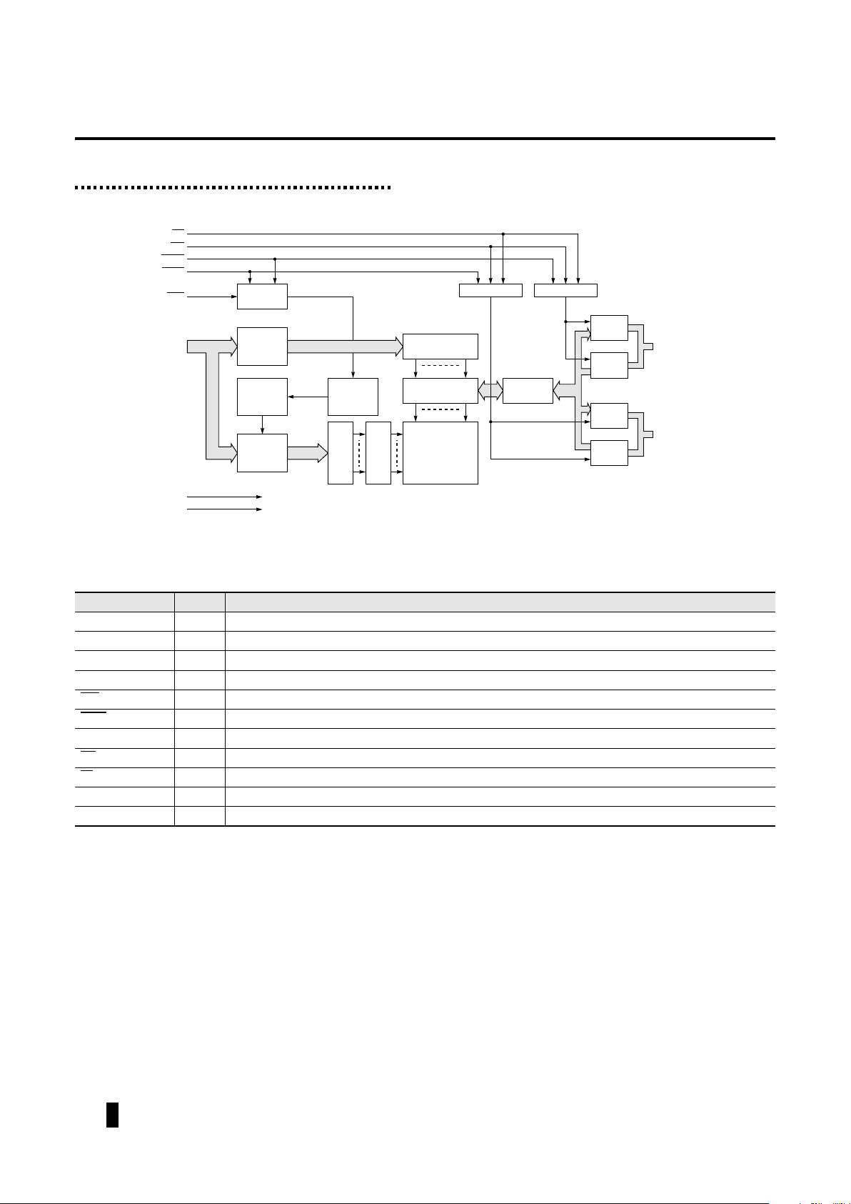
1. On-chip power supply to the EmDRAM should be separated from the Logic portion.
RAS
Timing
Generator
LCAS
Column
Address
Buffers
Internal
Address
Counter
Row
Address
Buffers
Refresh
Control
Clock
Column Decoders
Sense Amps
Memory Cells
Word Drivers
Row Decoders
A[8:0]
I/O Selector
Output
Buffer
Input
Buffer
DQ[15:8]
V
SS
V
CC
Output
Buffer
Input
Buffer
DQ[7:0]
UCAS
I/O Controller I/O Controller
WE
OE
Figure 1. GLT44016 - 256K X 16
Y[8:0]
X[8:0]
Signal Descriptions
[1]
Symbol
Type Description
DI[15:0] Input Data in.
DO[15:0] Output Data out.
XRA[7:0] Input Row address.
XCA[7:0] Input Column address.
RAS Input Row address strobe (active low).
CASH Input Column address strobe, access DI/DO[15:8] (active low)
CASL Input Column address strobe, access DI/DO[7:0] (active low)
WE Input Write enable (active low).
OE Input Output enable (active low).
V
DD
Supply 3.3v voltage supply, 2 pairs double bond minimum
V
SS
Supply Ground (voltage return), 2 pairs double bond minimum

3
G-LINK Technology
GLT41016-10E
May 1997 (Rev. 1)
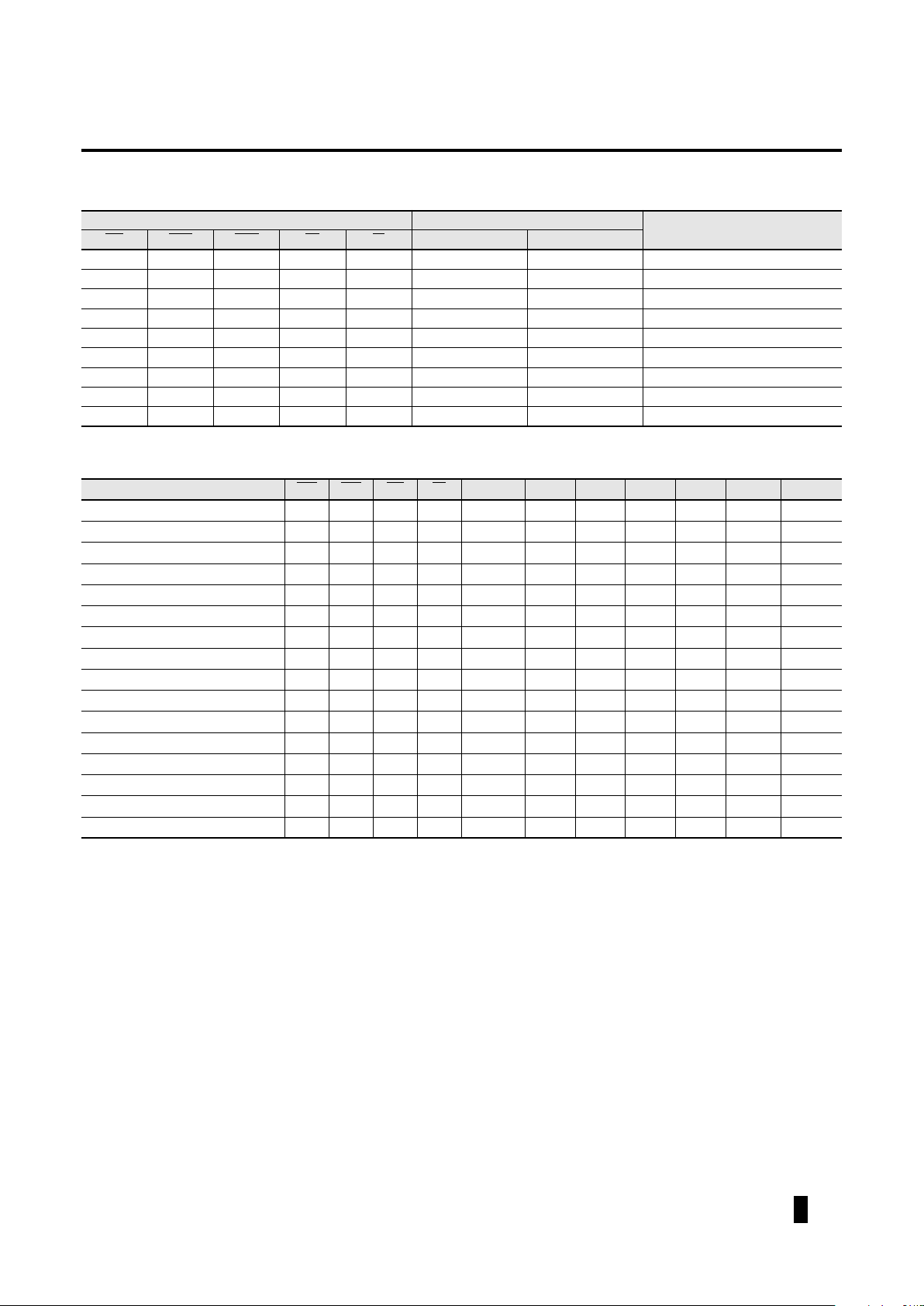
Function T able
Input Pin
DQ Pin
Functional ModeRAS LCAS UCAS WE OE DQ[7:0] DQ[15:8]
H–––– High-Z High-Z Standby
L H H – – High-Z High-Z Refresh
LLHHL D
OUT
High-Z Lower Byte Read
LHLHL High-Z Dout Upper Byte Read
L L L H L Dout Dout Word Read
LLHLH Din Don’t Care Lower Byte Write
L H L L H Don’t Care Din Upper Byte Write
LLLLH Din DinWord Write
L L L H H High-Z High Z –
T ruth Tab le
Function
RAS CAS WE OE Address DQM0 DQM1 DQM2 DQM3 DI[31:0] DO[31:0]
Standby H H X X X XXXX XHigh-Z
Read L L H L Row/Col XXXX XData Out
Write (Early) L L L X Row/Col HHHHData In High-Z
Write DI[7:0] L L L X Row/Col L H H H Data In High-Z
Write DI[15:8] L L L X Row/Col H L H H Data In High-Z
Write DI[23:16] L L L X Row/Col H H L H Data In High-Z
Write DI[31:24] L L L X Row/Col H H H L Data In High-Z
Read-Write L L H
→
LL
→
H Row/Col HHHHData In Data Out
Page-Mode Read (First Cycle) L H
→
L H L Row/Col XXXX XData Out
Page-Mode Read (Subsequent Cycles) H
→
LHLCol XXXX XData Out
Page-Mode Write (First Cycle) L H
→
L L X Row/Col HHHHData In High-Z
Page-Mode Write (Subsequent Cycle) L H
→
LLXCol HHHHData In High-Z
Page-Mode R-W (First Cycle) L H
→
LH
→
LL
→
H Row/Col HHHHData In Data Out
Page-Mode R-W (Subsequent Cycle) L H
→
LH
→
LL
→
HCol HHHHData In Data Out
CBR Refresh H
→
LLXX X XXXX XHigh-Z
RAS-only Refresh L H X X Row XXXX XHigh-Z

4
G-LINK Technology
GLT41016-10E
May 1997 (Rev. 1)
E
LECTRICAL
S
PECIFICATIONS
1. Permanent device damage may occur if ABSOLUTE MAXIMUM RATINGS are exceeded. Functional operation should be restricted to the conditions as detailed in the
operational sections of this data sheet. Exposure to absolute maximum rating conditions for extended periods may affect device reliability.
1. I
CC
Max. is specified for I
CC
for the output open condition.
2. Address can be changed once or less while RAS
= V
IL
.
3. Address can be changed once or less while CAS
= V
IH
.
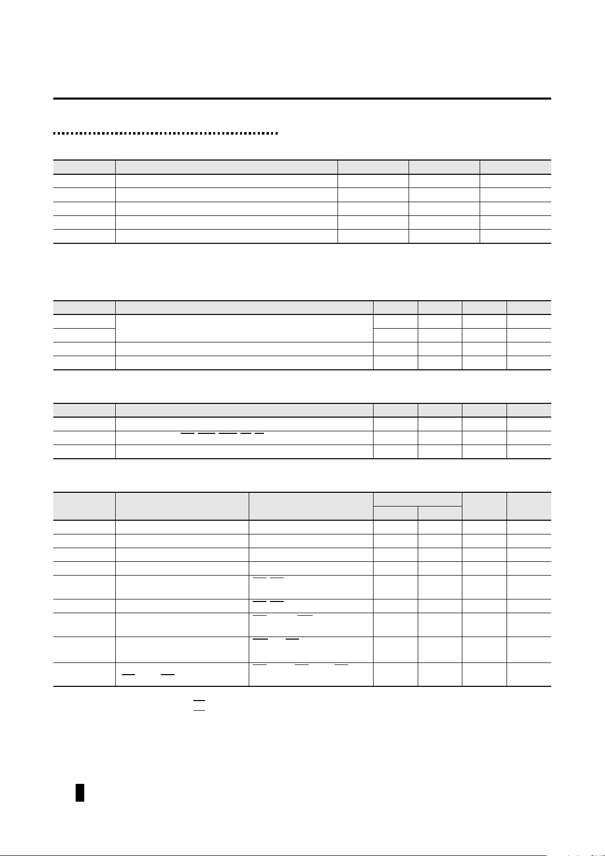
Absolute Maximum Ratings
[1]
Symbol
Parameter Conditions Value Unit
V
T
Voltage on any pin relative to V
SS
T
A
= 25 ˚C -0.5 to +4.6 V
I
OS
Short circuit output current T
A
= 25 ˚C 50 mA
P
D
Power dissipation T
A
= 25 ˚C 1 W
T
OPR
Operating temperature – 0 to +70
°
C
T
STG
Storage temperature – -55 to +150
°
C
Recommended Operating Conditions (T
A
= 0 ° C to +70 ° C)
Symbol
Parameter Min Typ Max Unit
V
CC
Power supply voltage 3.0 3.3 3.6 V
V
SS
000V
V
IH
Input high voltage 2.4 – V
CC
+1 V
V
IL
Input low voltage -1.0 – 0.8 V
Capacitance (V
CC
= 5V ± 10%, T
A
= 25 ° C, f = 1 MHz)
Symbol
Parameter Min Typ Max Unit
C
IN1
Input capacitance (A[8:0]) – 1 pF
C
IN2
Input capacitance (RAS
, LCAS, UCAS, WE, OE)–1pF
C
I/O
Input/Output capacitance (DQ[15:0]) – 1 pF
DC Characteristics (V
CC
= 5V ± 10%, T
A
= 0 ° C to +70 ° C)
Symbol
Parameter Condition
-30
Units
Note
Min Max
V
OH
Output High Voltage I
OH
= -2 mA 2.4 V
CC
V
V
OL
Output Low Voltage I
OL
= -1.0mA 0 0.4 V
I
LI
Input Leakage Current 0V
≤
V
IN
≤
V
CC
-2 -2
µ
A
I
LO
Output Leakage Current DQi Disable 0V
≤
V
O
≤
3.6V -10 -10
µ
A
I
CC1
Average Power Supply Current
(Operating)
RAS, CAS Cycling, t
RC
=Min. 200 mA
[1] [2]
I
CC2
Power Supply Current (Standby) RAS, CAS = V
IH
mA
[1]
I
CC3
Average Power Supply Current
(RAS-only Refresh)
RAS -Cycling, CAS = V
IH,
t
RC
= Min. 200 mA
[1] [2]
I
CC4
Average Power Supply Current
(Fast Page Mode)
RAS = V
IL,
CAS Cycling, t
HCP
= Min. 140 mA
[1] [3]
I
CC5
Average Power Supply Current
(CAS-before-RAS Refresh)
RAS Cycling, CAS-before-RAS 200 mA
 Loading...