

Page 1

250-Watt Gold Line Power Amplifier Issue 1, Rev. C: 10/21/96
Gold Line GL-T8500
250-Watt, 900-MHz Power Amplifier
USER MANUAL
PN 9110.0 0160 (old part number = 916-8500-000)
REV C
RELEASED
Specifications subject to change without notice
Copyright © 1996 Glenayre
All rights reserved. No part of this work may be reproduced or copied in any form or by
any means—graphic, electronic, or mechanical, including photocopying, recording,
taping, or information-ret rieva l system— without writte n perm issio n of Glenayre.
Print Date: 12/17/96 Copyright © 1996 Glenayre
Page 2

250-Watt Gold Line Power Amplifier Glenayre Do cument Number : 9110.00160
Document Change Record Issue 1, Rev. C: 10/21/96
Document Change Record
Revision: 0, Preliminary
Date: 05/04/95
Changes: none, original
Issue: Rev B
Date: 02/02/96
Changes: new format
Issue: Rev C
Date: 10/21/96
Changes: made released
Copyright © 1996 Glenayre Print Date: 12/17/96
Page 3

Glenayre Document Number: 9110.00160 250-Watt Gold Line Power Amplifier
Issue 1, Rev. C: 10/21/96 Table of Contents
Table of Contents
1 GENERAL . . . . . . . . . . . . . . . . . . . . . . . . . . . . . . . . . . . . 1-1
1.1 Manual Scope . . . . . . . . . . . . . . . . . . . . . . . . 1-1
1.2 Applicable Doc u ment s . . . . . . . . . . . . . . . . . . . . . 1-1
1.3 Manual Sections . . . . . . . . . . . . . . . . . . . . . . . 1-1
2 SPECIFICAT ION S . . . . . . . . . . . . . . . . . . . . . . . . . . . . . . . . 2-1
3 DESCRIPTION . . . . . . . . . . . . . . . . . . . . . . . . . . . . . . . . . . 3- 1
3.1 Introduction . . . . . . . . . . . . . . . . . . . . . . . . . 3-1
3.2 Physical Description. . . . . . . . . . . . . . . . . . . . . . 3 -1
3.2.1 Mounting Provisions . . . . . . . . . . . . . . . . . . . . . . . .3-1
3.2.2 PA Front. . . . . . . . . . . . . . . . . . . . . . . . . . . . . . .3-1
3.2.2.1 Driv e r Board . . . . . . . . . . . . . . . . . . . . . .3-1
3.2.2.2 PA Boards. . . . . . . . . . . . . . . . . . . . . . . .3-4
3.2.2.3 Combiner B oard . . . . . . . . . . . . . . . . . . . . . 3- 4
3.2.2.4 Metering Board . . . . . . . . . . . . . . . . . . . . .3 -4
3.2.3 PA Rear . . . . . . . . . . . . . . . . . . . . . . . . . . . . . . .3-4
3.2.3.1 Isolator . . . . . . . . . . . . . . . . . . . . . . . . .3-4
3.2.3.2 Fan . . . . . . . . . . . . . . . . . . . . . . . . . . .3 -4
3.3 Functional Description . . . . . . . . . . . . . . . . . . . . . 3-5
3.3.1 RF Amplifier . . . . . . . . . . . . . . . . . . . . . . . . . . . .3-5
3.3.2 Isolator . . . . . . . . . . . . . . . . . . . . . . . . . . . . . . . 3 -5
3.3.3 Metering . . . . . . . . . . . . . . . . . . . . . . . . . . . . . . .3- 6
4 INSTALL ATI ON AND SET UP . . . . . . . . . . . . . . . . . . . . . . . . . 4-1
4.1 Installation . . . . . . . . . . . . . . . . . . . . . . . . . 4-1
4.2 Setup. . . . . . . . . . . . . . . . . . . . . . . . . . . . 4-1
4.3 Ultimate Disposition . . . . . . . . . . . . . . . . . . . . . 4-1
5 OPERATIO N . . . . . . . . . . . . . . . . . . . . . . . . . . . . . . . . . . . 5-1
5.1 Controls and Indicators . . . . . . . . . . . . . . . . . . . . 5-1
5.2 Operation . . . . . . . . . . . . . . . . . . . . . . . . . . 5-1
5.2.1 Turn PA On and Off . . . . . . . . . . . . . . . . . . . . . . . .5 -1
3.2.3.3 Equipm ent Connectors . . . . . . . . . . . . . . . . . 3- 4
5.2.2 Turn Fan On and Off . . . . . . . . . . . . . . . . . . . . . . . .5-1
5.2.3 Key and Unkey PA . . . . . . . . . . . . . . . . . . . . . . . . .5-1
6 THEORY OF OPERATI ON . . . . . . . . . . . . . . . . . . . . . . . . . . . 6 -1
6.1 Power Distribu tio n . . . . . . . . . . . . . . . . . . . . . . 6 -1
6.1.1 Primary Power . . . . . . . . . . . . . . . . . . . . . . . . . . .6-1
Print Date: 12/17/96 Copyright © 1996 Glenayre Page: -i
Page 4

250-Watt Gold Line Power Amplifier Glenayre Do cument Number : 9110.00160
Table of Contents Issue 1, Rev. C: 10/21/96
6.1.1.1 Metering Board +25V Signal Flow. . . . . . . . . . . 6-1
6.1.1.2 Power Amplifiers +25V Signal Flow . . . . . . . . . . 6-1
6.1.2 Secondary Power . . . . . . . . . . . . . . . . . . . . . . . . . . 6-2
6.1.2.1 Metering Board +13.5V Signal Flow . . . . . . . . . . 6-2
6.1.2.2 Preamplifier Module +13.5V Signal Flow . . . . . . .6-2
6.1.3 Fan Power. . . . . . . . . . . . . . . . . . . . . . . . . . . . . . 6-2
6.2 RF Distribution . . . . . . . . . . . . . . . . . . . . . . . 6-3
6.2.1 Driver Board RF Flow . . . . . . . . . . . . . . . . . . . . . . . 6-3
6.2.2 PA Board RF Flow . . . . . . . . . . . . . . . . . . . . . . . . . 6-4
6.2.3 Combiner Board RF Flow . . . . . . . . . . . . . . . . . . . . .6-4
6.2.4 Isolator RF Flow . . . . . . . . . . . . . . . . . . . . . . . . . . 6-5
6.3 Control Di stri but i on . . . . . . . . . . . . . . . . . . . . . 6-5
6.3.1 AGC Signal Flow. . . . . . . . . . . . . . . . . . . . . . . . . . 6-5
6.3.2 Multiplexer Control Signal Flow . . . . . . . . . . . . . . . . . . 6-6
6.4 Status Distribut ion . . . . . . . . . . . . . . . . . . . . . . 6-6
6.4.1 Mux Analog Status Signal Flow . . . . . . . . . . . . . . . . . . 6-6
6.4.2 PA Fault Signal Flow. . . . . . . . . . . . . . . . . . . . . . . . 6-6
7 MAINTENANCE . . . . . . . . . . . . . . . . . . . . . . . . . . . . . . . . . 7-1
8 CHEC KOUT AND TROUBL ES HOOTI NG . . . . . . . . . . . . . . . . . . 8-1
9 REMOVAL AND REINST AL LAT ION . . . . . . . . . . . . . . . . . . . . 9-1
9.1 PA Chassis Removal and Reinstallation . . . . . . . . . . . . . 9-1
9.2 PA RF Module Removal and Reinstallation . . . . . . . . . . . . 9-1
9.3 Metering Board Removal and Reinstallation. . . . . . . . . . . . 9-1
Page: -ii Copyright © 1996 Glenayre Print Date: 12/17/96
Page 5

Glenayre Document Number: 9110.00160 250-Watt Gold Line Power Amplifier
Issue 1, Rev. C: 10/21/96 List of Figures
List of Figures
Figure 3-1 250-Watt, 900-MHz Power Amplif ier
Front View . . . . . . . . . . . . . . . . . . . . . . . . . . . . . . . . 3-2
Figure 3-2 250-Watt, 900-MHz Power Amplif ier
Rear View . . . . . . . . . . . . . . . . . . . . . . . . . . . . . . . . . 3- 3
Figure 3-3 PA Simplified-Block Diagram . . . . . . . . . . . . . . . . . . . . . . 3-5
Figure 5-1 Front-Panel Vie w wit h Cove r Rem o ved . . . . . . . . . . . . . . . . . 5-2
Figure 6-1 250-Watt PA Interconnection Diagram. . . . . . . . . . . . . . . . . . 6-8
Figure 6-2 250-Watt PA Functional Diagram . . . . . . . . . . . . . . . . . . . . 6-9
Figure 6-3 250-Watt PA Detailed Functional Diagram . . . . . . . . . . . . . . .6-10
Figure 6-4 Metering Board Functional Diagram . . . . . . . . . . . . . . . . . . . 6-12
Figure 9-1 PA Removal and Reinstalllation . . . . . . . . . . . . . . . . . . . . . 9-2
Figure 9-2 PA RF Module Removal and Reinstallation . . . . . . . . . . . . . . . 9-3
Figure 9-3 Metering Board Removal and Reinstallation . . . . . . . . . . . . . . . 9-5
Print Date: 12/17/96 Copyright © 1996 Glenayre Page: -iii
Page 6

250-Watt Gold Line Power Amplifier Glenayre Do cument Number : 9110.00160
List of Figures Issue 1, Rev. C: 10/21/96
Page: -iv Copyright © 1996 Glenayre Print Date: 12/17/96
Page 7

Glenayre Document Number: 9110.00160 250-Watt Gold Line Power Amplifier
Issue 1, Rev. C: 10/21/96 List of Tables
List of Tables
Table 1-1 Applicable Documents . . . . . . . . . . . . . . . . . . . . . . . . . . 1-1
Table 1-2 Manual Sections . . . . . . . . . . . . . . . . . . . . . . . . . . . . . 1-2
Table 2-1 Power Amplifier Specifications. . . . . . . . . . . . . . . . . . . . . . 2-1
Table 3-1 PA Circuit Boards. . . . . . . . . . . . . . . . . . . . . . . . . . . . . 3-1
Table 6-1 Multiplexer Analog Status Inputs. . . . . . . . . . . . . . . . . . . . . 6-7
Print Date: 12/17/96 Copyright © 1996 Glenayre Page: -v
Page 8

250-Watt Gold Line Power Amplifier Glenayre Do cument Number : 9110.00160
List of Tables Issue 1, Rev. C: 10/21/96
Page: -vi Copyright © 1996 Glenayre Print Date: 12/17/96
Page 9

Glenayre Document Number: 9110.00160 250-Watt Gold Line Power Amplifier
Issue 1, Rev. C: 10/21/96 GENERAL
1 GENERAL
1.1 Manual Scope
This manual provid es informa tion for the 250-watt, 9 00-MHz Gold Line powe r ampl ifier,
part number 265-0082-013. Also included is information for the optional triple isolator,
part number 7914.00010.
1.2 Applicable Documents
This manual is incomplete wi thout a dd iti on al Gol d Line ma nu als. R efer to Table 1-1 fo r a
listing and function of these manuals.
Table 1-1 Applicable Documents
document part number function
1.3 Manual Sections
GL-T8500/8600 system manual
VDT manual 9110.00164 describes PA contro l so ftwa re
exciter manual 9110.00172 describes exci ter/ PA cont ro l
250-watt PA 9110.00160 this manual
power supply manual 9110.00159 describes 50A/ 90A pow er suppl y
Table 1-2 lists the section s of thi s man u a l wit h a summary of thei r cont en t s.
9110.00163 describes fully racke d-up G old
Line tr an smitt er
installed in exciter
equipment in transmitter
equipment in transmitter
Print Date: 12/17/96 Copyright © 1996 Glenayre Page: 1-1
Page 10

250-Watt Gold Line Power Amplifier Glenayre Do cument Number : 9110.00160
GENERAL Issue 1, Rev. C: 10/21/96
Table 1-2 Manual Sections
section contents
1. General introduct ion and purpose of manu al
2. Specificatio ns significa nt measu rem ent s of power am plifie r
3. Descripti on introdu ction and princi pal charac teristics of power
amplifier
4. Installation and Setup initial installation and activation of power amplifier
5. Operation operation of power amplifier
6. Theory of Operati on detailed func tiona l d esc ript ion of circ u itry wi thi n
power amplifier
7. Mainten ance proced ure s to be performe d on specifi c int erv al s to
maintain optimum performance of power amplifier
8. Checkout and Troubleshooting verification of proper operation, correction to proper
operation of power amplifier
9. Removal and Reinst alla tio n replacemen t proce dure s for power am pli fie r and
selected subassemblies
Page: 1-2 Copyright © 1996 Glenayre Print Date: 12/17/96
Page 11

Glenayre Document Number: 9110.00160 250-Watt Gold Line Power Amplifier
Issue 1, Rev. C: 10/21/96 SPECIFICATIONS
2 SPECIFICATIONS
Table 2-1 lists the significant equipment-level specifications for the Gold Line power
amplifier.
Table 2-1 Power Amplifie r Specificatio n s
measurem ent specification
height 8.75 in (22.23 cm)
width 19 in (48.3 cm)
depth 8 in (20.3 cm)
weight 26 lb (12 kg)
RF output power 100 - 250 watts
RF bandwidth 900 - 960 MHz
RF input power 200 - 400 mW
RF impedance 50 ohms
operating voltages 25 vdc, 25 Vdc, 13.5 Vdc
PA 25 Vdc current 72 mA - 33 A
fan 25 Vdc current 750 m A
13.5 Vdc current 3.3 A
ambient temperature -30° - +70° C
humidity 0 - 95% noncondensing
altitude to 10,000 ft (3050 m)
Print Date: 12/17/96 Copyright © 1996 Glenayre Page: 2-1
Page 12

250-Watt Gold Line Power Amplifier Glenayre Do cument Number : 9110.00160
SPECIFICATIONS Issue 1, Rev. C: 10/21/96
Page: 2-2 Copyright © 1996 Glenayre Print Date: 12/17/96
Page 13

Glenayre Document Number: 9110.00160 250-Watt Gold Line Power Amplifier
Issue 1, Rev. C: 10/21/96 DESCRIPTION
3 DESCRIPTION
3.1 Introduction
Figure 3-1, 250-Watt, 900-MHz Power Amplifier Front View, and Figure 3-2, 250-Watt,
900-MHz Power Amplifier Rear View,show th e Gold Line power amplifi er (PA). This is a
250-watt PA intended for use in a GL-T8500 paging transmitter with an RF of 900 MHz
nominal. Th is PA is characteri zed by int egrated mon itoring dev ices that suppl y critical
status informat ion to a Gold Li ne exciter/ PA control (exciter). This exci ter contains d iagnostic softw a re that can dete ct and report a fault y PA circuit board.
3.2 Physical Description
3.2.1 Mounting Provisions
The P A is mounted to the front of most standar d 19-inch equipment racks by means of eight
screws. The fron t panel of the PA may by removed wh ile the PA is mounted in the rack.
T wo quarter-turn fasteners secure the front panel to the PA. Most PA circuit boards may be
replaced while the PA is mounted in the rack.
3.2.2 PA Front
Figure 5-1 shows the front view of the PA with the front pa nel removed. This expos es the
RF and shielded compartments, which contain the PA circuit boards. Table 3-1 lists the PA
circuit boards.
Table 3-1 PA Circuit Boards
nomencla ture part number location
driver board A1 263-0082-022 RF compartment
PA1 board A2 263-0082-007 RF compartment
PA2 board A3 263-0082-007 RF compartment
combiner board A4 263-0082-021 RF compartment
metering board A5 263-0082-018 shielded compartment
3.2.2.1 Driver Board
The driver board (A1) contain s the preamp module, the intermediate PA (IPA), and the PA
drivers (driver-1 and driver-2). These device s, in addition to on e resistor, are mounted
directly o n th e PA heat sink. T he dr i v er board co nta i ns three co n n ec to rs: t w o o n t h e f ron t
(J1 and J2) and one on the back (J3). Two RG316-type cables (not shown) are attached to
the front of the board.
Print Date: 12/17/96 Copyright © 1996 Glenayre Page: 3-1
Page 14
250-Watt Gold Line Power Amplifier Glenayre Do cument Number : 9110.00160
DESCRIPTION Issue 1, Rev. C: 10/21/96
v0222.hgl
Figure 3-1 250-Watt, 900-MHz Power Amplifier
Front View
Page: 3-2 Copyright © 1996 Glenayre Print Date: 12/17/96
Page 15

Glenayre Document Number: 9110.00160 250-Watt Gold Line Power Amplifier
Issue 1, Rev. C: 10/21/96 DESCRIPTION
v0221.hgl
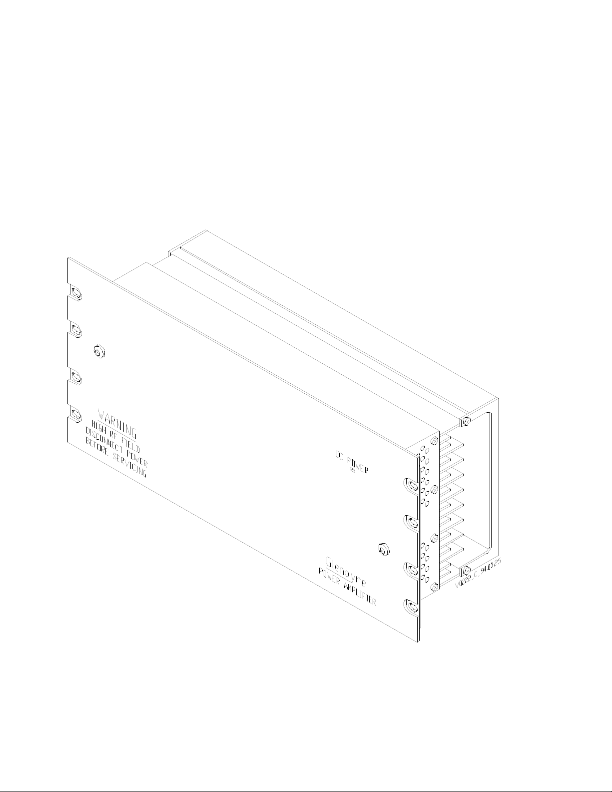
Figure 3-2 250-Watt, 900-MHz Power Amplifier
Rear View
Print Date: 12/17/96 Copyright © 1996 Glenayre Page: 3-3
Page 16

250-Watt Gold Line Power Amplifier Glenayre Do cument Number : 9110.00160
DESCRIPTION Issue 1, Rev. C: 10/21/96
3.2.2.2 PA Boards
Two PA boards, PA1 (A2) and PA2 (A3), contain the power amplifiers. The PA boards are
identical but are mounte d with different orientations. Each PA board conta ins an A and a B
pair of power amplifiers. These amplifiers and six resistors are mounted directly on the PA
heat sink. Conn ect ors J1 and J3 and an RG142-type ca ble (not sh own) are attached to the
front of each board.
3.2.2.3 Combiner Board
The combin e r bo ard comb i nes th e outpu t s of the PA boards. The comb i ner bo a rd con t ain s
a resistor, mounted directly on the PA heat sink. Connectors J1, J2, and J3 are on the front
of the board. An RG 393-t ype cable is atta ched to the ba ck of the board . This cable terminates with a type-N connector and extends through t he rear of the PA.
3.2.2.4 Metering Board
The metering boar d contai ns the monitori ng circui ts for the PA. A bank of nine aut omoti ve
spade-ty pe fu se s prot ec t the PA. A transist o r is mounted di rec tl y on th e PA heat sink . The
metering board contains connectors J1, J2, J4, J5, and P1 on the front and J3 on the back.
The board contains one LED (DC POWER).
3.2.3 PA Rear
Figure 3-2 sh ow s the back view of the PA. The PA back pan el c onc eals the fan c ompart-
ment. The isolator and fan are mounted on the back panel. The PA equipment connectors
terminate on cables that are routed through grommeted holes in the back panel.
3.2.3.1 Isolator
The s ta n da rd iso l at o r (s how n ) i mp ro ves the i nt ermodu l at io n perform a nc e o f th e PA by 25
dB. This isolat or is mounted on its own heat si nk , wh ich extends i nto t he fan compartment .
The optional triple isola tor (not shown ) improves the interm odulation performance of the
P A by 75 dB, and is mounted on the PA. Both isolators contains three connectors: two typeN and one BNC.
3.2.3.2 Fan
A si ngle fa n pr ovides cool ing for the PA and sta nda r d is olat or. T he f an i s lo c at ed w i th i n the
fan compartment and is covered by a finger guard. The fan runs co ntinuously whenever
power is applied by the power supply equipment.
3.2.3.3 Equipment Connectors
There are five equipment connectors in addition to those on the isolator. Two 1/4-inch ring
lugs are desi g nat ed a s plus (red) a n d mi n us (black). A 9-pin plug-an d-socket con nect or i s
designated as P2. A DB15-type connector is designated as PA CONTROL. A BNC
connector is designated as P3.
Page: 3-4 Copyright © 1996 Glenayre Print Date: 12/17/96
Page 17

Glenayre Document Number: 9110.00160 250-Watt Gold Line Power Amplifier
A
A
A
A
A
A
A
A
A
A
A
A
A
A
A
A
A
A
A
A
A
A
A
A
A
A
A
A
A
A
A
Issue 1, Rev. C: 10/21/96 DESCRIPTION
3.3 Functional Description
Figure 3-3 shows a si mplifi ed, func ti onal diagr am of t he PA. The driver, comb iner , and PA
boards constitute the RF amplifier circuitry of the PA. Monitoring and controlling this RF
amplifier is the metering board. Figure 3-1 shows the RF amplifier, is olator, and meteri ng
circuit ry within the PA.
BNC
RF
IN
1/4 LUGS
DC
IN
25V
13.5V
AA
AA
AA
AA
AA
AA
AA
AA
AA
AA
AA
AA
AA
AA
P2
METERED
POWER
RF
AMPLIFIER
STATUS
VOLTAGES
METERING
POWER
AMPLIFIER
TYPE N TYPE N
AA
AA
AA
AA
AA
AA
AA
AAA
AAA
ISOLATOR
AAAA
AAAA
BNC
AA
AA
AA
AA
AA
AA
AA
VSWR
SAMPLE
AA
AA
STATU S/
AA
AA
AA
AA
CONTROL
AA
DB-15
RF
OUT
3.3.1 RF Amplifie r
3.3.2 Isolator
Figure 3-3 PA Simplified-Block Diagram
The RF amplifie r receives its RF i nput thro ugh the BNC co nnector P3. A detecto r circuit
in the RF amplifier monitors this RF input. The RF input is amplified by means of four
amplifier stages. Each amplifier stage receives its dc input power through the metering
circuit. Power detectors at critical locations throughout the RF amplifier provide sample
voltages to th e me terin g circ u it. Th e amplified output of the RF amplifier is appli ed to the
input type-N con nector on the isolator.
The isolator prevents intermodulation of the RF signal that may occur from nearby transmissions. The RF signal is routed through input and output type N connectors. A detector
circuit in the isolator moni tors the reflected power (VSW R) present at the ou tput type-N
connector. A sample voltage representing the VSWR level is output through the BNC
connector. The opt ion al t ripl e iso lat o r fu nctio n s id ent ical ly t o t he s ta nda rd is olato r e xcept
with a higher level of intermodulat ion prevention.
Print Date: 12/17/96 Copyright © 1996 Glenayre Page: 3-5
Page 18

250-Watt Gold Line Power Amplifier Glenayre Do cument Number : 9110.00160
DESCRIPTION Issue 1, Rev. C: 10/21/96
3.3.3 Metering
The me terin g boa rd perf o rms co ntro l and st atu s repo rtin g for the PA. The meteri ng bo ard
accepts a 25-Vdc power input through the 1/4-inch lugs and a 13.5-Vdc power input
through connector P2. These voltages are regulated and distributed.
Page: 3-6 Copyright © 1996 Glenayre Print Date: 12/17/96
Page 19

Glenayre Document Number: 9110.00160 250-Watt Gold Line Power Amplifier
Issue 1, Rev. C: 10/21/96 INSTALLATION AND SETUP
4 INSTALLATION AND SETUP
4.1 Installation
The PA is shipped alre ady insta lled in a cabin et. To remove or rei nstall t he PA, refer to
Section 9.
4.2 Setup
Setup of the PA is performed at the system level using an exciter/PA control unit. Refer to
the GL-T8500 system manual. The system manual includes instructions for these
applicable setup procedures:
• adjust forward power
• set low power alarm
• calibrate reflected power
4.3 Ultimate Disposition
Caution
This equipment may contain hazardous materials.
Check with the local EPA or other environmental
authority before disposing of this equipment.
Print Date: 12/17/96 Copyright © 1996 Glenayre Page: 4-1
Page 20

250-Watt Gold Line Power Amplifier Glenayre Do cument Number : 9110.00160
INSTALLATION AND SETUP Issue 1, Rev. C: 10/21/96
Page: 4-2 Copyright © 1996 Glenayre Print Date: 12/17/96
Page 21

Glenayre Document Number: 9110.00160 250-Watt Gold Line Power Amplifier
Issue 1, Rev. C: 10/21/96 OPERATION
5 OPERATION
5.1 Controls and Indicators
The PA has one indicator and no controls. Figure 5-1, Front-Panel View with Cover
Remo ved shows the location of the PA indicator LED1.
5.2 Operation
5.2.1 Turn PA On and Off
The PA does not contain an on/of f switch, but turns on and off whenever the power supply
equipment is turned on and off. When the PA is on, it remains in a standby condition until
keyed. Refe r to the pow er su ppl y man u al for turn -o n and turn-off procedu res.
5.2.2 Turn Fan On and Off
The fan doe s not contain an on/off swi tch, bu t turns on an d off whenever the p ow er supply
equipment is turned on and off. The fan runs continuously whenever the power supply
equipmen t is on. Re f e r to the po w e r su pply manual fo r tu rn-on an d tu rn - o ff pr o cedures.
5.2.3 Key and Unkey PA
The PA does not contain a key switch, but is keyed and unkeye d by the exciter/PA control
equipment. This exciter must be keyed and unkeyed remotely through transmitter
controller, or locally through a video display terminal (VDT). Refer to the controller
manual for remote key and unkey instru ctions, or to the VDT manual for local key and
unkey instruc ti ons.
Print Date: 12/17/96 Copyright © 1996 Glenayre Page: 5-1
Page 22

250-Watt Gold Line Power Amplifier Glenayre Do cument Number : 9110.00160
OPERATION Issue 1, Rev. C: 10/21/96
v0224.hgl
Figure 5-1 Front-Pane l View with Cover Rem oved
Page: 5-2 Copyright © 1996 Glenayre Print Date: 12/17/96
Page 23

Glenayre Document Number: 9110.00160 250-Watt Gold Line Power Amplifier
Issue 1, Rev. C: 10/21/96 THEORY OF OPERATIO N
6 THEORY OF OPERATION
6.1 Power Distribution
The PA requires three separate power inputs: primary 25-volt dc power, secondary 13.5volt dc pow er, and fan 25-volt d c power. All power i nputs are n ormally provided by the
Gold Line power supply.
6.1.1 Primary Power
Refer to Figure 6-2. Primary 25-volt dc operati ng power is receive d through the powe r
cables termin ating wi th 1/4-inch ring lugs . The ( - ) inpu t (bla ck c abl e) is bolted directl y to
PA chassis ground. The (+) input (red cable) is bolted to P1 on the metering board . P1
powers the +25V power bus on the me terin g board. Thi s bus distri bu tes p rimary powe r to
the metering board an d to eac h common-b a se co l lect o r (C BC ) po we r am pli f ie r in the PA.
6.1.1.1 Metering Board +25V Signal Flow
Refer to Figure 6-4. +25 volts from the power bus is supplied through fuse F13 to these
places on the meterin g board : LED 1, +25V components, divider circuitry, +5V regulator
and di v ider circuitry, and +1.2V regulator circuitry.
• LED1 activates to illuminate the DC POWER indicator on the front of the PA.
• +25V components receive operating power. These components include the current
detector amp l ifie rs.
• Divider circuit reduces the input to a sample voltage, which determines the PA 25V
meteri ng.
• +5V regulator/divider circui try generates +5V operating power for the metering board
+5V components. A portion of this +5V is reduced to a sample voltage, which determines the PA 5V metering.
• +1.2V regul ator circuitry generates the compensa tion voltage for the curren t detector
amplifiers.
6.1.1.2 Power Amplifiers +25V Signal Flow
Refer to Figure 6-1. +25 volts operating power from the power bus is paralleled through
seven resistors. Th es e resi stors are a compon ent of a current detec tio n circu it.
Current-Detection Theo ry
Current-det ecti on monitorin g occurs on the me tering boa rd. The moni tore d current is
routed through a sma ll res ist or, resu lt i ng in a slig ht vol ta ge dro p across the resist o r.
This voltage drop is amplified by a current detector amplifier, which generates an output voltage proportional to the current flowing through the resistor. This output voltage
is the current sample for the monito re d current .
Print Date: 12/17/96 Copyright © 1996 Glenayre Page: 6-1
Page 24

250-Watt Gold Line Power Amplifier Glenayre Do cument Number : 9110.00160
THEORY OF OPERATION Issue 1, Rev. C: 10/21/96
The seven mon itored +25-vol t signals are indi vidually fused before leavin g the metering
board. The signals provide operating power for power amplifiers located on the driver and
PA boards. Each signal is routed through a dc bias network.
Dc-Bias Network Theory
Dc bias networks are locat ed on the driver boa rd and PA board s. +25-v olt operat ing
power from the metering board is applied to the power amplifiers through a dc bias network . T he n etwor k is t une d and f iltere d t o cause a hi gh im p eda nc e to si gnals fr om dc to
above operating frequency. This prevents RF from transmitting backwards into the metering board.
6.1.2 Secondary Power
Seco nda ry 13 .5-v ol t dc pow er f or t he PA is ex ter nal ly fu se d, at the pow er su pply e qui pment. Refer to Figure 6-1. Secondary power is received through connector P2, which
mates w i th J 2 o n the system interco n n ect harne ss. Secon da ry power is connected to J 5 o n
the metering boa rd. The +13.5 input from J5 is distributed to the met ering board and the
preamp module.
6.1.2.1 Metering Board +13.5V Signal Flow
Refer to Figure 6-2. +13.5-volt power from J5 is paralleled to these places on the metering
board: +13.5V components, divider circuitry, and heat sink temperature trans duc er U17.
• +13.5V component s receive operat ing power. Th ese compon ents include those wit hin
the AGC integrator circuit.
• Divider circuit reduces the input to a sample voltage, which determines the system PA
13.5V metering.
• Heat-sink-temperature transducer U17 generates a vol tage proportional to the tempe ra-
ture of the PA heat sink, which determines the temperature metering.
6.1.2.2 Preamplifier Module +13.5V Signal Flow
Refer to Figure 6-2. +13.5-volt power fr om J5 is r ou ted thr o ugh a resi st or , a component of
a current-detection circuit. The sample provided by this circuit determines the preamplifier
current metering. The +13.5-volt power through the resistor is fused by F4 before distribution to the meterin g boa rd an d preampl ifi er mo dul e, on the dri ver boa rd.
6.1.3 Fan Power
25-volt dc fan power is fused externally at the power supply equipment. Refer to Figure 6-
1. Fan power is received through connector P2, which mates with J2 on the system inter-
connect harness. Fan powe r is applied directly to the fan via a qu ick-release jack (not
shown).
Page: 6-2 Copyright © 1996 Glenayre Print Date: 12/17/96
Page 25

Glenayre Document Number: 9110.00160 250-Watt Gold Line Power Amplifier
Issue 1, Rev. C: 10/21/96 THEORY OF OPERATION
6.2 RF Distribution
Refer to Figure 6-1. The PA RF input is received through a BNC connector, which mates
with J3 on the exciter/PA control. This RF input signal (at a nominal 350 mW) is split and
amplified into two RF signals (at a nominal 40 watts) by the driver board. Each RF signal
is amplifie d (to a nom inal 150 watts ) by a PA board. These RF signals are c ombin ed i nto
one RF signal (at a nominal 275 watts) by the combiner board. This is the PA RF output,
and is applie d to an isolator. The isolator R F output (at a n omin al 250 wa tts for st andard)
is sup p li ed t o an ante nna fo r trans mis s ion. A ll p ower l ev el s give n her e and in t he f ol lo wing
paragraphs are typica l; actual powe r level s wil l vary from tho se given .
6.2.1 Driver Board RF Flow
The driver bo ard splits and amplifies a 350-mW RF inpu t into two 40-watt RF outputs.
Refer to Figure 6-3. The RF i nput to the dr iver board i s ap pli ed to t he preampli fier modul e
(Q1). A portion of the RF input is appli ed to an RF-detec tion circuit on the boa rd. This
circuit rectifie s and filt er s the RF inp ut into an OK s ignal. Loss of the RF input and the OK
signal resu l ts in an exci te r output fault.
The preamplifier module is a three-stage RF power amplifier on a single IC. The first and
third stages are powered by an AGC signal. These are the variable gain stages, and control
the forward power output of the PA. The first and third stages of the preamp module are
powered by an AGC signal, generated on the metering board. AGC signal voltage is
monitored for status only. The second stage of the preamplifier module is a nonvariablegain stage, powered by +13. 5-volt power. The current draw n by the AG C and +13.5-vo lt
power signal s contribu t es to the preampli f ier curre n t meteri ng .
The amplified RF outpu t from t h e preamp module is appli e d to t he IPA (Q2). The current
drawn from the IPA’s +25-volt powe r source is mon itored to determine the IPA current
metering. The amplified RF output from the IPA is monitored for forward and reflected
power levels. The power sampl es detected at this location determine the IPA forward - and
reflected-po wer me terin g.
Power-Moni toring Theory
Power-m on i tor circ u it s are loca t ed on th e driv er boa rd, PA boa rd s, an d com bin e r
board. A microstrip line parallel to the RF signal path couples a small portion of the ac
signal ac ross a rectifier and filtering circuit. The ac signal may be rectified to detect either the forward or reflected power. After filtering, a dc sample voltage is available that
is proportional to the power detected at the monitored location.
Print Date: 12/17/96 Copyright © 1996 Glenayre Page: 6-3
Page 26

250-Watt Gold Line Power Amplifier Glenayre Do cument Number : 9110.00160
THEORY OF OPERATION Issue 1, Rev. C: 10/21/96
After monitoring, the amplified RF output from the IPA is split in two by means of an RF
splitter, common ly known as a Wilkinson splitter. The two split RF sig nals are appl ied to
driver-1 (Q3) and driver-2 (Q4). The current draw n from each driver ’s +25-volt power
source is monitored to determine the driver-1 and driver-2 current metering. The amplified
RF outputs from the two drivers are the driver board’s 40-watt RF outputs.
Wilkinson Spl itter/ Co m biner Th eor y
Wilkinson splitter and combiner networks are located in the RF signal path on the driver board, PA boa rd s, an d combiner board . A wa ste r resi sto r is lo c ated a pre ci se dis tance from th e sig n al jun c ti o n . Th is resistor dissipate s any o ut-of-pha se im ba la n ce or
amplifier imbalance that may exist between the RF signals being split or combined, resulting in a more sta ble am plifier.
6.2.2 PA Board RF Flow
Each P A board a mplifies a 40-watt RF input into a 150-watt RF output. Refer to Figure 6-
3. The RF input to the P A board is split into four signals by means of three Wilkinson split-
ters. Each RF signal drives a power amplifier, for a total of four amplifiers (Q1, Q2, Q3,
and Q4). Q1 and Q2 receive operating power from a common +25-volt power source. The
current drawn by thi s source is monitored to det ermine the PA board’s A-pair curren t.
Likewise, the current drawn by Q3 and Q4 common +25-volt power source is monitored to
determin e the PA board’s B-pair current.
The amplified RF out puts from the four power amplifiers are c ombined into one by mean s
of three Wilkinson combiners. The RF signal from the last Wilkinson combiner is
monitored for forward and reflected power levels. The power samples detected at this
location determine the PA board’s forward and reflected power metering. The combined
and monitored RF signal is the PA board’s 150-watt RF output.
6.2.3 Combiner Board RF Flow
The combiner board combines two 150-watt RF inputs into a single 275-watt RF output.
Refer to Figure 6-3. The two RF inputs are com bined by a Wilkinson combiner. The
combined RF is monitored for forward power level. The power sample detected at this
loca ti on det er mi n es the t ota l f or war d p ow er me te r in g. Th e com b i ned an d mo ni to r e d sig na l
is the combiner board’s 275-watt RF output.
6.2.4 Isolator RF Flow
The isolator conducts its 275-watt RF input only in the forward direction, suppressing any
intermodulation or VSWR present at its RF output. Refer to Figure 6-3. The RF input is
applied throu gh a circulato r. The optional triple isolator RF inpu t is applied thro ugh three
circulators.
Circulator Th eor y
A circulator consists of several circular layers of copper, ferrite, and a magnetic material that biases th e ferrit e. The circ ula tor ha s th ree inpu t s/ou t put s. The biase d ferrit e co nducts electric ity only in one dire ction , outpu ttin g the signa l appli ed at its previou s
input. Each circulator prov id es 25 d B of isola ti on.
Page: 6-4 Copyright © 1996 Glenayre Print Date: 12/17/96
Page 27

Glenayre Document Number: 9110.00160 250-Watt Gold Line Power Amplifier
Issue 1, Rev. C: 10/21/96 THEORY OF OPERATION
The circulato r RF ou tput i s applied throu gh a notc h filt er to rem ove the seco nd harmo nic s
generated by the circulator. This filtered RF is the isolator’s RF output. This RF output is
ty pica lly 250 wa tts for a stan dard i solator o r 225 watt s for a tripl e isolat or. Any reflected
power present at the isolator RF output is conducted back through the circulator to a
rectifier and filtering circuit. This circuit generates a dc sample voltage proportional to the
VSWR present a t the isolator RF o utput. The sample vo l tage d etermines the to t al r ef l ec tedpower metering.
6.3 Control Distribution
Refer to Figure 6-1. The PA control inputs are received through a DB15 connector, which
mates with J6 on the exciter/PA control. Two ty pes of control inputs are received: AGC
referenc e and mul ti ple xer.
6.3.1 AGC Signal Flow
The metering board c ompares the AGC referenc e signal (from the exciter) wi th the total
forward power sample (from the combiner board) to create an AGC signal (to the driver
board). Refer to Figure 6-2. The AGC reference signal and the total forward power sample
are applied t o an integ rator circu it, which ge nerates the AGC signa l. An increa se in the
AGC refere nce si gn al or a decre ase in th e tota l forw ard po wer sa mple causes an in crease
in the AGC signal. This AGC signal provides operating power for the first and third
amplifie r stag e s of the pre am pli fier. Divider c ircu i try red uce s a port ion of th e AG C sig nal
to a sample voltage, which determines the AGC metering.
6.3.2 Multiplexer Control Signal Flow
6.4 Status Distribution
Analog Multiplexer Theory
Three analog multiplexers are located on the metering board. Each multiplexer receives as many as eight analog inputs, at a sample voltage which represents a PA parameter or status. Control lines from the exciter command the multiplexer to connect
one of the inputs to a common output, which is measured by the exciter. The multiplexer is switched quickly between the analog inputs, resulting in a multiplexed analog
output.
Refer to Figure 6-2. The exciter controls each multiplexer by four control lines: three
address lines and a lat ch. The addres s lines (0, 1, a nd 2) are binary signals wi th a total of
eight possible states. The address lines sequence through the eight states in about 360
microse conds. A s each s tate occurs, the la tch line i s toggled, selectin g the an alog input
corresponding to that address state. The voltag e present at the multiplexer commo n out put
is the most recently latched analog input.
Refer to Figure 6-1. The PA status outputs are supplied through the same DB15-type
connector as the PA control inputs, which mates with J6 on the exciter/PA control. Two
types of status outputs are supplied: multiplexed (mux) analog and PA fault.
Print Date: 12/17/96 Copyright © 1996 Glenayre Page: 6-5
Page 28

250-Watt Gold Line Power Amplifier Glenayre Do cument Number : 9110.00160
THEORY OF OPERATION Issue 1, Rev. C: 10/21/96
6.4.1 Mux Analo g Stat us Sig nal Flow
Mux analog status signals consist of dc voltages that repres ent a paramete r or fault within
the PA. These s ignals are ge nerated by c urrent detecto rs, power mon itors, and mete ring
dividers, which supply a status voltage propo rtional to the leve l of parameter i t is representing, or the existence of the fault it is representing. Refer to Figure 6-2. These status
voltages are applied to one of the three multiplexers located on the metering board. The
multiplexers ro u te t he a ppro pria te st at us v olt age t o the ex cit er i n the fo rm o f mu x a n alo g.
Table 6-1 lis ts a ll s tatus vo lta ge nom enc latur e, the mu lt ipl exer that rou tes t ha t vo lta ge , a nd
the control address that directs the multiplexer to route that voltage.
6.4.2 PA Fault Signal Flow
A PA fault signal is activated when a reflected power threshold is exceeded by the PA1 or
P A2 board. Refer to Figure 6-2. A port ion o f the P A 1 boa rd an d PA2 board re flect ed p ower
status voltages are applied to a comparator and switching circuit. When either status
exceeds a voltage repre senting a bout 20 watts, the switch is activa ted. Th e switch appl ies
a PA fault to the exciter, which shuts down the transmitter.
Table 6-1 Multiplexer Analog Status Inputs
addr multiplexer 1 multiplexer 2 multiplexer 3
000 PA1-A current preamp current total forward power
001 PA1-B current IPA current (no input)
010 PA2-A current driver-1 current IPA forward power
011 PA2-B current driver-2 current IPA reflected powe r
100 PA1 forward power (no input) +25V voltage level
101 reflected power (no input) +13.5V voltage level
110 PA2 forw ard power exciter output fault +5V voltage level
111 PA2 reflected power AGC voltage level PA heat sink temp
Page: 6-6 Copyright © 1996 Glenayre Print Date: 12/17/96
Page 29

Glenayre Document Number: 9110.00160 250-Watt Gold Line Power Amplifier
Issue 1, Rev. C: 10/21/96 THEORY OF OPERATION
v0229.hgl
Figure 6-1 250-Watt PA Interconnection Diagr am
Print Date: 12/17/96 Copyright © 1996 Glenayre Page: 6-7
Page 30

250-Watt Gold Line Power Amplifier Glenayre Do cument Number : 9110.00160
THEORY OF OPERATION Issue 1, Rev. C: 10/21/96
v0203.hgl
Figure 6-2 250-W att PA Functional Diagram
Page: 6-8 Copyright © 1996 Glenayre Print Date: 12/17/96
Page 31

Glenayre Document Number: 9110.00160 250-Watt Gold Line Power Amplifier
Issue 1, Rev. C: 10/21/96 THEORY OF OPERATION
v0202l.hgl
Figure 6-3 2 50-Watt PA Detailed Functional Diagram
Print Date: 12/17/96 Copyright © 1996 Glenayre Page: 6-9
Page 32

250-Watt Gold Line Power Amplifier Glenayre Do cument Number : 9110.00160
THEORY OF OPERATION Issue 1, Rev. C: 10/21/96
v0202r.hgl
250-Watt PA Detailed Functional Diagram
Page: 6-10 Copyright © 1996 Glenayre Print Date: 12/17/96
Page 33

Glenayre Document Number: 9110.00160 250-Watt Gold Line Power Amplifier
Issue 1, Rev. C: 10/21/96 THEORY OF OPERATION
v0204l.hgl
Figure 6-4 Metering Bo ard Functi onal Diagr am
Print Date: 12/17/96 Copyright © 1996 Glenayre Page: 6-11
Page 34

250-Watt Gold Line Power Amplifier Glenayre Do cument Number : 9110.00160
THEORY OF OPERATION Issue 1, Rev. C: 10/21/96
0204r.hgl
Metering Board Functional Diagram
Page: 6-12 Copyright © 1996 Glenayre Print Date: 12/17/96
Page 35

Glenayre Document Number: 9110.00160 250-Watt Gold Line Power Amplifier
Issue 1, Rev. C: 10/21/96 MAINTENANCE
7 MAINTENANCE
Refer to the system and VDT manuals.
Print Date: 12/17/96 Copyright © 1996 Glenayre Page: 7-1
Page 36

250-Watt Gold Line Power Amplifier Glenayre Do cument Number : 9110.00160
MAINTENANCE Issue 1, Rev. C: 10/21/96
Page: 7-2 Copyright © 1996 Glenayre Print Date: 12/17/96
Page 37

Glenayre Document Number: 9110.00160 250-Watt Gold Line Power Amplifier
Issue 1, Rev. C: 10/21/96 CHECKOUT AND TROUBLESHOOTING
8 CHECKOUT AND TROUBLESHOOTING
Refer to the system and VDT manuals.
Print Date: 12/17/96 Copyright © 1996 Glenayre Page: 8-1
Page 38

250-Watt Gold Line Power Amplifier Glenayre Do cument Number : 9110.00160
CHECKOUT AND TROUBLESHOOTING Issue 1, Rev. C: 10/21/96
Page: 8-2 Copyright © 1996 Glenayre Print Date: 12/17/96
Page 39

Glenayre Document Number: 9110.00160 250-Watt Gold Line Power Amplifier
Issue 1, Rev. C: 10/21/96 REMOVAL AND REINSTALLATION
9 REMOVAL AND REINSTALLATION
9.1 PA Chassis Removal and Reinstallation
Figure 9-1 sh o w s d etails of removin g an d reinstall i ng t h e c h assis. Cal ibration of fo rward
and reflected power is required after reinstallation.
9.2 PA RF Module Removal and Reinstallation
Figure 9-2 shows details of removing and reinst al ling P A RF modules.
9.3 Metering Board Removal and Reinstallation
Figure 9-3 shows details of removing and reinstalling the metering board.
Print Date: 12/17/96 Copyright © 1996 Glenayre Page: 9-1
Page 40

250-Watt Gold Line Power Amplifier Glenayre Do cument Number : 9110.00160
REMOVAL AND REINSTALLATION Issue 1, Rev. C: 10/21/96
v0223.hgl
Figure 9-1 PA Removal and Reinstalllation
Page: 9-2 Copyright © 1996 Glenayre Print Date: 12/17/96
Page 41

Glenayre Document Number: 9110.00160 250-Watt Gold Line Power Amplifier
Issue 1, Rev. C: 10/21/96 REMOVAL AND REINSTALLATION
Print Date: 12/17/96 Copyright © 1996 Glenayre Page: 9-3
Page 42

250-Watt Gold Line Power Amplifier Glenayre Do cument Number : 9110.00160
REMOVAL AND REINSTALLATION Issue 1, Rev. C: 10/21/96
v0225.hgl
Figure 9-2 PA RF Module Removal a nd Reinst all ati on
Page: 9-4 Copyright © 1996 Glenayre Print Date: 12/17/96
Page 43

Glenayre Document Number: 9110.00160 250-Watt Gold Line Power Amplifier
Issue 1, Rev. C: 10/21/96 REMOVAL AND REINSTALLATION
Figure 9-2 PA R F Module Removal and Reinstallation (continue d)
Print Date: 12/17/96 Copyright © 1996 Glenayre Page: 9-5
Page 44

250-Watt Gold Line Power Amplifier Glenayre Do cument Number : 9110.00160
REMOVAL AND REINSTALLATION Issue 1, Rev. C: 10/21/96
v0228.hgl
Figure 9-3 Metering Board Removal and Reinstallation
Page: 9-6 Copyright © 1996 Glenayre Print Date: 12/17/96
Page 45

Glenayre Document Number: 9110.00160 250-Watt Gold Line Power Amplifier
Issue 1, Rev. C: 10/21/96 REMOVAL AND REINSTALLATION
v0227.hgl
Figure 9-3 Metering Board Removal and Reinstallation (continued)
Print Date: 12/17/96 Copyright © 1996 Glenayre Page: 9-7
Page 46

250-Watt Gold Line Power Amplifier Glenayre Do cument Number : 9110.00160
REMOVAL AND REINSTALLATION Issue 1, Rev. C: 10/21/96
Page: 9-8 Copyright © 1996 Glenayre Print Date: 12/17/96
 Loading...