

Page 1

Overview
1.
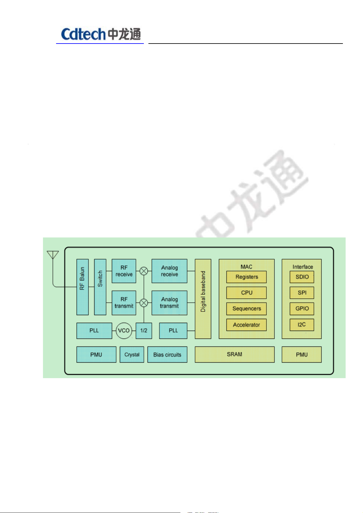
The ES8266 A1T1 offers a complete and s
to either host the application or to offload all Wi-Fi networking functions from another application
processor.
When The ES8266 A1T1 hosts the application, and when it is the only application processor in
the device, it is able to boot up directly from an external flash. It has integrated cache to improve
the performance of the system in such applications, and to minimize the memory requirements.
Alternately, serving as a Wi-Fi adapter, wireless internet access can be added to any
microcontroller-based design with simple connectivity through UART interface or the CPU
AHB bridge interface.
The ES8266 A1T1 on-board proc
the sensors and other application specific devices through its GPIOs with minimal development
up-front and minimal loading during runtime. With its high degree of on-chip integration, which
includes the antenna switch balun, power management converters, it requires minimal external
essing and storage capabilities allow it to be integrated with
elf-contained Wi-Fi networking solution, allowing it
circuitry, and the entire solution, including front-end module, is designed to occupy minimal PCB
area.
Sophisticated system-level features include fast sleep/wake context switching for energy-
efficient VoIP, adaptive radio biasing for low-power operation, advance signal processing, and
spur cancellation and radio co-existence features for common cellular, Bluetooth, DDR, LVDS,
LCD interference mitigation.
2. Features
•
802.11 b/g/n protocol
•
Wi-Fi Direct (P2P), soft-AP
•
Integrated TCP/IP protocol stack
•
Integrated TR switch, balun, LNA, power amplifier and matching network
•
Integrated PLL, regulators, and power management units
•
+18.5dBm output power in 802.11b mode
•
Integrated temperature sensor
Page 2
•
Supports antenna diversity
•
Power down leakage current of < 10uA
•
Integrated low power 32-bit CPU could be used as application processor
•
SDIO 2.0, SPI, UART
•
STBC, 1×1 MIMO, 2×1 MIMO
•
A-MPDU & A-MSDU aggregation & 0.4µs guard interval
•
Wake up and transmit packets in < 2ms
•
Standby power consumption of < 1.0mW (DTIM3)
3. Block Diagram
4.General Specification
Page 3
Model
Product Name WI-Fi 11b/g/n 1T1R
Major Chipset Esp8266
Standard 802.11b/g/n
Data Transfer Rate maximum of 72.2Mbps
Modulation Method BPSK/ QPSK/ 16-QAM/ 64-QAM
Frequency Band 2.4~2.4835 GHz ISM Band
ES8266 A1T1
Spread Spectrum
RF Output Power
Operation Mode Ad hoc, Infrastructure
WLAN Receiver
Sensitivity
Operation Range Up to 180 meters in open space
OS Support Win7 32/64,Win8 32/64,Android
Security WEP, TKIP, AES, WPA, WPA2
Interface SDIO 2.0
Power Consumption DC 3.3V Maximum power dissipation in 600mA
Operating
Temperature
Storage Temperature -40 ~ 85°C ambient temperature
IEEE 802.11b: DSSS (Direct Sequence Spread Spectrum) IEEE
802.11g/n:OFDM (Orthogonal Frequency Division Multiplexing)
11n > 12dBm,11g > 13dBm,11b > 16dBm
11b CCK11(PER<8%) < -85dBm , 11g OFDM54(PER<10%) <
-72dBm , 11n HT20 MCS7(PER<10%) < -69dBm ,
-20~ +60° C ambient temperature
Humidity 5 to 90 % maximum (non-condensing)
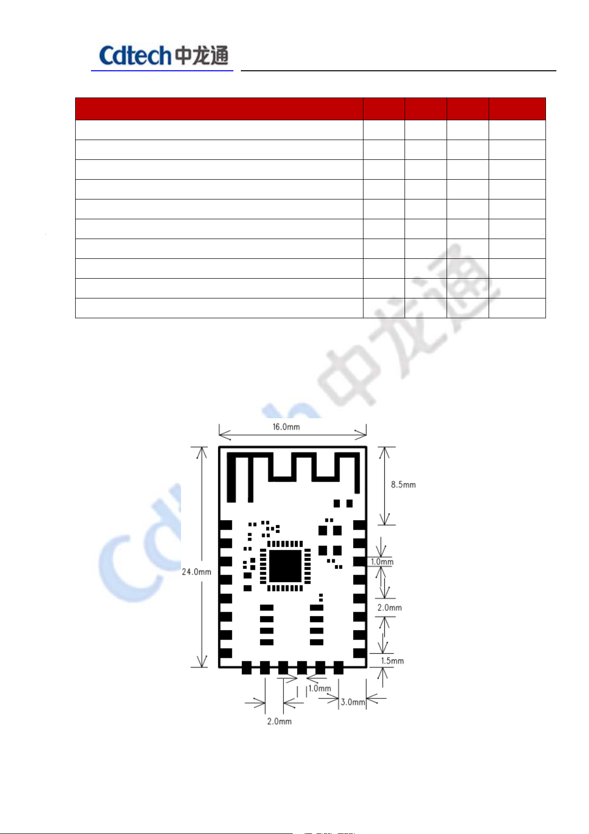
Dimension 24*16mm (LxW) +-0.2MM
5.DC Characteristics
Page 4
Mode Min
Typ
Ma
x
Uni
t
Transmit 802.11b, CCK 11Mbps, P
Transmit 802.11g, OFDM 54Mbps, P
Transmit 802.11n, MCS7, P
Receive 802.11b, packet length=1024 byte, -80dBm
Receive 802.11g, packet length=1024 byte, -70dBm
Receive 802.11n, packet length=1024 byte, -65dBm
Modem-Sleep
Light-Sleep
Deep-Sleep
Off 5
OUT
=+13dBm
OUT
OUT
=+17dBm
=+15dBm
170
140
120
WLAN current consumption
Note: All result is measured at the antenna port and VDD33 is 3.3V
6. Pin Description and PCB size
mA
mA
mA
50 mA
56 mA
56 mA
15 mA
0.9 mA
10 uA
uA
Page 5

NO Name Description
1
2
3
4
5
6
7
8
9
10
11
12
13
14
15
16
RST
ADC ADC
EN
GPIO16
GPIO14
GPIO12
GPIO13
VCC 3.3V
CS0
MISO
GPIO9
GPIO10
MOSI
SCLK
GND
GPIO15
Reset
Chip enable, active high
Chip Select
17
18
19
20
21
22
Operating mode
UART
GPIO2
GPIO0
GPIO4
GPIO5
RXD UART RXD
TXD UART TXD
下载
Flash boot
GPIO0 GPIO2 GPIO15
低高 低
高高 低
Page 6
7.Modular
对应物料 型号规格 供应厂家
Crystal 26Mhz
PCBA VER 132-8782660-00 怡科通,博敏
晶威特,福晶
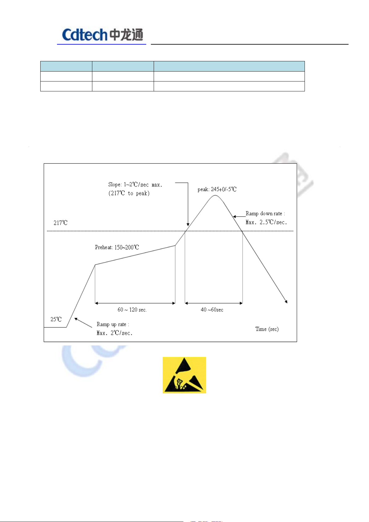
8. Recommended Reflow Profile
Referred IPC/JEDEC standard.
Peak Temperature : <250°C
Number of Times : 2times
ESD CAUTION
The ES8266 A1T1 is ESD (electrostatic discharge) sensitive dev
damaged with ESD or spike v
tion circuitry, please handle with care to avoid the permanent malfunction or the
protec
performance degradation.
oltage. Although ES8266 A1T1 is with built-in ESD
ice and may be
Page 7
This device is intended only for OEM integrators under the following conditions:
1) The antenna must be installed such that 20 cm is maintained between the antenna
and users, and
2) The transmitter module may not be co-located with any other transmitter or antenna,
3) For all products market in US, OEM has to limit the operation channels in CH1 to
CH11 for 2.4G band by supplied firmware programming tool. OEM shall not supply
any tool or info to the end-user regarding to Regulatory Domain change.
As long as 3 conditions above are met, further transmitter test will not be required.
However, the OEM integrator is still responsible for testing their end-product for any
additional compliance requirements required with this module installed
The host will Satisfy Class I or Class Ⅱ permissive change based this module FCC ID.
If the FCC identification number is not visible when the module is installed inside the host, then
the outside of the device into which the module is installed must also display a label referring to
the enclosed module. This exterior label can use wording such as the following: “Contains
Transmitter Module Contains FCC ID:2ASLM-ES8266A1T1 or “Contains FCC ID:2ASLM-
ES8266A1T1 .Any similar wording that expresses the same meaning may be used.
20C
 Loading...