

Giga-tronics GT 9000 Operation & Maintenance Manual

Manual Number : 120AM00250
Revision: C
Configuratio n Code: 14
Print Date : September 1998
Operation & Maintenance Manual
Model GT 9000
Microwave Synthesizer
. . . . . . . . . . . . . . . . . . . . . . . . . . . . . . . . . . . . . . . . . . . Certified Product
ISO 9001
Registra: BSI, Certification No. FM 34226, Registered 04 June 1996
Giga-tronics Incorporated ❖ 4650 Norris Canyon Road ❖ San Ramon, California 94583
Telephone (925) 328-4650, or (800) 726-4442 ❖ Telefax (925) 328-4700
Customer Service: Telephone (800) 444-2878 ❖ Telefax (925) 328-4702
. . . . . . . . . . . . . . . . . . . . . . . . . . . . . . . . Certified Process
Web Site: www.gigatronics.com

All technical data and specifications in this manual are subject to change without prior notice and
do not represent a commitment on the part of Giga-tronics Incorporated.
© Copyright Giga-tron ics Incorporated 1998. All rights reserved .
Printed in U.S.A.
WARRANTY
Giga-tronics products are warranted against defective materials and
workmanship for one year from date of shipment. Giga-tr onics will at its
option repair or replace products that are proven defective during the
warranty period. This warranty DOES NOT cover damage resulting from
improper use, nor workmanship other than Giga- tronics service. There is
no implied warranty of fitness for a particular purpose, nor is
Giga-tronics liable for any consequential damages. Specification and
price change privileges are reserved by Giga-tronics.
Giga-tronics Service Contacts
Territory Primary Contact Secondary Contact
Customer Service: USA & Canada (800) 444-2878
Pacific Rim & Far East (800) 444-2878
Europe & South Africa (800) 444-2878
Applications and Technical
Support:
All Territories (800) 726-4142
(925) 328-4646
(925) 328-4646
(925) 328-4646
(925) 328-4665
(800) 726-4442
(925) 328-4660
(800) 726-4442
(925) 328-4670
(800) 726-4442
(925) 328-4664
(800) 726-4442
(925) 328-4669

Table of Contents
About This Manual . . . . . . . . . . . . . . . . . . . . . . . . . . . . . . . . . . . . . . . . . . . . . . xi
Convent ions. . . . . . . . . . . . . . . . . . . . . . . . . . . . . . . . . . . . . . . . . . . . . . . . . . . . xiii
Record of Man ual Changes . . . . . . . . . . . . . . . . . . . . . . . . . . . . . . . . . . . . . . . xv
Special Con figurations . . . . . . . . . . . . . . . . . . . . . . . . . . . . . . . . . . . . . . . . . . . xvii
1 • Intro ductio n_______________________________________________________
1.1 General Information. . . . . . . . . . . . . . . . . . . . . . . . . . . . . . . . . . . . . . . . . . . . . . . . . . . . . . . . 1-1
1.1.1 Introduction . . . . . . . . . . . . . . . . . . . . . . . . . . . . . . . . . . . . . . . . . . . . . . . . . . . . . . . . 1-1
1.1.2 Items Furnished . . . . . . . . . . . . . . . . . . . . . . . . . . . . . . . . . . . . . . . . . . . . . . . . . . . . 1-2
1.1.3 Items Requi red. . . . . . . . . . . . . . . . . . . . . . . . . . . . . . . . . . . . . . . . . . . . . . . . . . . . . 1-2
1.1.4 Tools and Test Equipment . . . . . . . . . . . . . . . . . . . . . . . . . . . . . . . . . . . . . . . . . . . 1-2
1.1.5 Cooling . . . . . . . . . . . . . . . . . . . . . . . . . . . . . . . . . . . . . . . . . . . . . . . . . . . . . . . . . . . 1-2
1.1.6 Cleaning . . . . . . . . . . . . . . . . . . . . . . . . . . . . . . . . . . . . . . . . . . . . . . . . . . . . . . . . . . 1-2
1.1.7 Installation and Prepara tion for Use . . . . . . . . . . . . . . . . . . . . . . . . . . . . . . . . . . . . 1-2
1.1.8 Receivin g Inspection . . . . . . . . . . . . . . . . . . . . . . . . . . . . . . . . . . . . . . . . . . . . . . . . 1-2
1.1.9 Preparat ion for Reship ment. . . . . . . . . . . . . . . . . . . . . . . . . . . . . . . . . . . . . . . . . . . 1-3
1.2 Safety Precautions . . . . . . . . . . . . . . . . . . . . . . . . . . . . . . . . . . . . . . . . . . . . . . . . . . . . . . . . 1-4
1.2.1 Voltage and Fuse Selection . . . . . . . . . . . . . . . . . . . . . . . . . . . . . . . . . . . . . . . . . . 1-5
1.3 Performance Specifications. . . . . . . . . . . . . . . . . . . . . . . . . . . . . . . . . . . . . . . . . . . . . . . . . . 1-6
1.3.1 CW O p eration . . . . . . . . . . . . . . . . . . . . . . . . . . . . . . . . . . . . . . . . . . . . . . . . . . . . . 1-6
1.3.2 Spectral Pur ity . . . . . . . . . . . . . . . . . . . . . . . . . . . . . . . . . . . . . . . . . . . . . . . . . . . . . 1-6
1.3.3 RF O u tput Power . . . . . . . . . . . . . . . . . . . . . . . . . . . . . . . . . . . . . . . . . . . . . . . . . . . 1-7
1.3.4 PM Envelope Parameters . . . . . . . . . . . . . . . . . . . . . . . . . . . . . . . . . . . . . . . . . . . . 1-7
1.3.5 Internally Generated PM Repetition Rate . . . . . . . . . . . . . . . . . . . . . . . . . . . . . . . . 1-8
1.3.6 Internally G enerated PM Delay. . . . . . . . . . . . . . . . . . . . . . . . . . . . . . . . . . . . . . . . 1-8
1.3.7 Internally Generated PM Width . . . . . . . . . . . . . . . . . . . . . . . . . . . . . . . . . . . . . . . . 1-8
1.3.8 Externally Tri ggered PM Envelop e . . . . . . . . . . . . . . . . . . . . . . . . . . . . . . . . . . . . . 1-8
1.3.9 Externally Ge nerated PM Enve lope . . . . . . . . . . . . . . . . . . . . . . . . . . . . . . . . . . . . 1 - 8
1.3.10 FM Envelope Param eters (Wide or Narrow Mode) . . . . . . . . . . . . . . . . . . . . . . . . 1-9
1.3.11 FM Envelope Param eters (Wide Mode) . . . . . . . . . . . . . . . . . . . . . . . . . . . . . . . . . 1-9
1.3.12 FM Envelope Param eters (Narrow Mode) . . . . . . . . . . . . . . . . . . . . . . . . . . . . . . . 1-9
1.3.13 FM Indicator. . . . . . . . . . . . . . . . . . . . . . . . . . . . . . . . . . . . . . . . . . . . . . . . . . . . . . . 1-9
1.3.14 Internally Generated FM Enve l o pe (O ption 24 only) . . . . . . . . . . . . . . . . . . . . . . . 1-9
1.3.15 Externa lly Supplied FM Envelope . . . . . . . . . . . . . . . . . . . . . . . . . . . . . . . . . . . . . . 1-10
1.3.16 Amplitud e Modulation . . . . . . . . . . . . . . . . . . . . . . . . . . . . . . . . . . . . . . . . . . . . . . . 1-10
1.3.17 AM Indicat o r . . . . . . . . . . . . . . . . . . . . . . . . . . . . . . . . . . . . . . . . . . . . . . . . . . . . . . . 1-10
1.3.18 Internally Generated AM Envelope . . . . . . . . . . . . . . . . . . . . . . . . . . . . . . . . . . . . . 1-10
1.3.19 External l y Supplied AM Envelope . . . . . . . . . . . . . . . . . . . . . . . . . . . . . . . . . . . . . . 1-11
1.3.20 External Automatic Level Cont rol . . . . . . . . . . . . . . . . . . . . . . . . . . . . . . . . . . . . . . 1-11
1.3.21 Front Panel Inputs/Outputs . . . . . . . . . . . . . . . . . . . . . . . . . . . . . . . . . . . . . . . . . . . 1-11
1.3.22 Rear Panel Inputs/Output s . . . . . . . . . . . . . . . . . . . . . . . . . . . . . . . . . . . . . . . . . . . 1-11
1.3.23 General Specificati o ns. . . . . . . . . . . . . . . . . . . . . . . . . . . . . . . . . . . . . . . . . . . . . . . 1-12
2 • Opera tion _________________________________________________________
2.1 Introduction . . . . . . . . . . . . . . . . . . . . . . . . . . . . . . . . . . . . . . . . . . . . . . . . . . . . . . . . . . . . . . 2-1
2.2 The Front Panel. . . . . . . . . . . . . . . . . . . . . . . . . . . . . . . . . . . . . . . . . . . . . . . . . . . . . . . . . . . 2-1
Manual No. 120AM00250, Rev C, September 1998
i

Series GT 9000 Microwave Synthesizers
2.2.1 Entry Menu . . . . . . . . . . . . . . . . . . . . . . . . . . . . . . . . . . . . . . . . . . . . . . . . . . . . . . . . 2-2
2.2.2 Data Entry Field . . . . . . . . . . . . . . . . . . . . . . . . . . . . . . . . . . . . . . . . . . . . . . . . . . . . 2-3
2.2.3 Shifted Functions . . . . . . . . . . . . . . . . . . . . . . . . . . . . . . . . . . . . . . . . . . . . . . . . . . . 2-5
2.2.4 Frequency . . . . . . . . . . . . . . . . . . . . . . . . . . . . . . . . . . . . . . . . . . . . . . . . . . . . . . . . . 2-8
2.2.5 RF Level . . . . . . . . . . . . . . . . . . . . . . . . . . . . . . . . . . . . . . . . . . . . . . . . . . . . . . . . . . 2-9
2.2.6 Pulse Modula tion . . . . . . . . . . . . . . . . . . . . . . . . . . . . . . . . . . . . . . . . . . . . . . . . . . . 2-10
2.2.7 Frequency Modulation . . . . . . . . . . . . . . . . . . . . . . . . . . . . . . . . . . . . . . . . . . . . . . . 2-12
2.2.8 Amplitude Modulation . . . . . . . . . . . . . . . . . . . . . . . . . . . . . . . . . . . . . . . . . . . . . . . . 2-14
2.3 The Rear Panel . . . . . . . . . . . . . . . . . . . . . . . . . . . . . . . . . . . . . . . . . . . . . . . . . . . . . . . . . . . 2-16
2.3.1 BNCs. . . . . . . . . . . . . . . . . . . . . . . . . . . . . . . . . . . . . . . . . . . . . . . . . . . . . . . . . . . . . 2-16
2.3.2 Line Power and Fuse . . . . . . . . . . . . . . . . . . . . . . . . . . . . . . . . . . . . . . . . . . . . . . . . 2-17
2.3.3 IEEE-488 Int erface . . . . . . . . . . . . . . . . . . . . . . . . . . . . . . . . . . . . . . . . . . . . . . . . . . 2-17
2.4 GT 9000 Syntax . . . . . . . . . . . . . . . . . . . . . . . . . . . . . . . . . . . . . . . . . . . . . . . . . . . . . . . . . . . 2-19
2.4.1 GT 9000 Syntax Virtual K e ystrokes. . . . . . . . . . . . . . . . . . . . . . . . . . . . . . . . . . . . . 2-24
2.5 1026 Syntax Interface . . . . . . . . . . . . . . . . . . . . . . . . . . . . . . . . . . . . . . . . . . . . . . . . . . . . . . 2-25
2.5.1 Character Representa tion . . . . . . . . . . . . . . . . . . . . . . . . . . . . . . . . . . . . . . . . . . . . 2-25
2.5.2 Command Format. . . . . . . . . . . . . . . . . . . . . . . . . . . . . . . . . . . . . . . . . . . . . . . . . . . 2-25
2.5.3 Commands . . . . . . . . . . . . . . . . . . . . . . . . . . . . . . . . . . . . . . . . . . . . . . . . . . . . . . . . 2-26
3 • Theo ry of Oper ation ________________________________________________
3.1 Introduction. . . . . . . . . . . . . . . . . . . . . . . . . . . . . . . . . . . . . . . . . . . . . . . . . . . . . . . . . . . . . . . 3-1
3.2 General Circuit T heory. . . . . . . . . . . . . . . . . . . . . . . . . . . . . . . . . . . . . . . . . . . . . . . . . . . . . . 3-1
3.2.1 The Compute r . . . . . . . . . . . . . . . . . . . . . . . . . . . . . . . . . . . . . . . . . . . . . . . . . . . . . . 3-2
3.2.2 The RF Path . . . . . . . . . . . . . . . . . . . . . . . . . . . . . . . . . . . . . . . . . . . . . . . . . . . . . . . 3-3
3.2.3 Phase Lock Loops . . . . . . . . . . . . . . . . . . . . . . . . . . . . . . . . . . . . . . . . . . . . . . . . . . 3-3
3.2.4 Dual-Loop Indirect Synthesis . . . . . . . . . . . . . . . . . . . . . . . . . . . . . . . . . . . . . . . . . . 3-5
3.2.5 The Output Loop. . . . . . . . . . . . . . . . . . . . . . . . . . . . . . . . . . . . . . . . . . . . . . . . . . . . 3-6
3.2.6 The Reference Loop. . . . . . . . . . . . . . . . . . . . . . . . . . . . . . . . . . . . . . . . . . . . . . . . . 3-8
3.2.7 The Downcon verter . . . . . . . . . . . . . . . . . . . . . . . . . . . . . . . . . . . . . . . . . . . . . . . . . 3-12
3.2.8 Level Control. . . . . . . . . . . . . . . . . . . . . . . . . . . . . . . . . . . . . . . . . . . . . . . . . . . . . . . 3-15
3.2.9 Frequency Modulation . . . . . . . . . . . . . . . . . . . . . . . . . . . . . . . . . . . . . . . . . . . . . . . 3-17
3.2.10 Amplitud e Modulation . . . . . . . . . . . . . . . . . . . . . . . . . . . . . . . . . . . . . . . . . . . . . . . . 3-17
3.2.11 Pulse Modul a tion . . . . . . . . . . . . . . . . . . . . . . . . . . . . . . . . . . . . . . . . . . . . . . . . . . . 3-17
3.3 Assembly Circ uit Descriptions . . . . . . . . . . . . . . . . . . . . . . . . . . . . . . . . . . . . . . . . . . . . . . . . 3-18
3.3.1 Front Panel Inte rface — PC Assembly A1 . . . . . . . . . . . . . . . . . . . . . . . . . . . . . . . 3-18
3.3.2 IEEE / T IMER — PC Assembly A2 . . . . . . . . . . . . . . . . . . . . . . . . . . . . . . . . . . . . . 3-18
3.3.3 Memory — PC Assembl y A3 . . . . . . . . . . . . . . . . . . . . . . . . . . . . . . . . . . . . . . . . . . 3-19
3.3.4 CPU — P C Assembly A4. . . . . . . . . . . . . . . . . . . . . . . . . . . . . . . . . . . . . . . . . . . . . 3-20
3.3.5 Pulse Driver — PC Assemb ly A5. . . . . . . . . . . . . . . . . . . . . . . . . . . . . . . . . . . . . . . 3-20
3.3.6 Pulse Generat o r — PC Assembly A5A1 . . . . . . . . . . . . . . . . . . . . . . . . . . . . . . . . . 3-21
3.3.7 AM/FM Driver — PC Assemb ly A6 . . . . . . . . . . . . . . . . . . . . . . . . . . . . . . . . . . . . . 3-21
3.3.8 Fu nc tion Generator — PC Assembly A6A1. . . . . . . . . . . . . . . . . . . . . . . . . . . . . . . 3-22
3.3.9 Scan Modulati on — PC Assem b ly A 7 . . . . . . . . . . . . . . . . . . . . . . . . . . . . . . . . . . . 3-22
3.3.10 Level — PC Assembly A10 . . . . . . . . . . . . . . . . . . . . . . . . . . . . . . . . . . . . . . . . . . . 3-23
3.3.11 Level Driver — PC Assembly A10A1 . . . . . . . . . . . . . . . . . . . . . . . . . . . . . . . . . . . 3-24
3.3.12 Power Supply — PC Assembly A11 . . . . . . . . . . . . . . . . . . . . . . . . . . . . . . . . . . . . 3-25
3.3.13 100 MHz Reference PLL — PC Assembl y A14 . . . . . . . . . . . . . . . . . . . . . . . . . . . 3-26
3.3.14 1 Hz PLL — PC Assembly A15 . . . . . . . . . . . . . . . . . . . . . . . . . . . . . . . . . . . . . . . . 3-27
3.3.15 Reference / Downconverter PLL — PC Assembly A16 . . . . . . . . . . . . . . . . . . . . . 3-28
3.3.16 Divide-By- N — PC Assembly A 17 . . . . . . . . . . . . . . . . . . . . . . . . . . . . . . . . . . . . . . 3-30
3.3.17 Output PLL — PC Assembly A18 . . . . . . . . . . . . . . . . . . . . . . . . . . . . . . . . . . . . . . 3-32
3.3.18 YIG Driver — PC Assembl y A19 . . . . . . . . . . . . . . . . . . . . . . . . . . . . . . . . . . . . . . . 3-33
3.3.19 Display Drive r — PC Assembly A 20 . . . . . . . . . . . . . . . . . . . . . . . . . . . . . . . . . . . . 3-33
ii
Manual No. 120AM00250, Rev C, September 1998

Preface
3.3.20 Pushbutt o n — PC Assembly A105 . . . . . . . . . . . . . . . . . . . . . . . . . . . . . . . . . . . . . 3-33
3.3.21 Data Entry — PC Assembly A106 . . . . . . . . . . . . . . . . . . . . . . . . . . . . . . . . . . . . . 3-34
3.3.22 Main Tune — PC Assembly A107 . . . . . . . . . . . . . . . . . . . . . . . . . . . . . . . . . . . . . 3-34
3.3.23 Detector Buffer — PC Assembly A200. . . . . . . . . . . . . . . . . . . . . . . . . . . . . . . . . . 3-34
3.3.24 100 MHz Oscillator/ Sampler Driver — PC Assembly A20 1. . . . . . . . . . . . . . . . . . 3-35
4 • Cali bration a nd Testi ng_____________________________________________
4.1 Calibration Procedur es . . . . . . . . . . . . . . . . . . . . . . . . . . . . . . . . . . . . . . . . . . . . . . . . . . . . . 4-1
4.1.1 Recommended Equipment: . . . . . . . . . . . . . . . . . . . . . . . . . . . . . . . . . . . . . . . . . . . 4-1
4.1.2 Power Supply Calibratio n . . . . . . . . . . . . . . . . . . . . . . . . . . . . . . . . . . . . . . . . . . . . 4-2
4.1.3 100 MHz Phase Lock Loop . . . . . . . . . . . . . . . . . . . . . . . . . . . . . . . . . . . . . . . . . . . 4-3
4.1.4 Sampler Drive rs, 100 MHz VCO (Optional) . . . . . . . . . . . . . . . . . . . . . . . . . . . . . . 4- 3
4.1.5 YIG Driver Calib ration . . . . . . . . . . . . . . . . . . . . . . . . . . . . . . . . . . . . . . . . . . . . . . . 4-4
4.1.6 Level Calibration . . . . . . . . . . . . . . . . . . . . . . . . . . . . . . . . . . . . . . . . . . . . . . . . . . . 4-5
4.1.7 AM/FM Generator Verificat i on (O ption 24 only) . . . . . . . . . . . . . . . . . . . . . . . . . . . 4-6
4.1.8 Pulse Genera tor Verification . . . . . . . . . . . . . . . . . . . . . . . . . . . . . . . . . . . . . . . . . 4-7
4.1.9 AM Calibrati on . . . . . . . . . . . . . . . . . . . . . . . . . . . . . . . . . . . . . . . . . . . . . . . . . . . . . 4-8
4.1.10 FM Calibrat ion . . . . . . . . . . . . . . . . . . . . . . . . . . . . . . . . . . . . . . . . . . . . . . . . . . . . . 4-9
4.1.11 Spectral Purity . . . . . . . . . . . . . . . . . . . . . . . . . . . . . . . . . . . . . . . . . . . . . . . . . . . . . 4-10
4.1.12 10 MHz Time Base . . . . . . . . . . . . . . . . . . . . . . . . . . . . . . . . . . . . . . . . . . . . . . . . . 4-10
4.2 Performance Tests . . . . . . . . . . . . . . . . . . . . . . . . . . . . . . . . . . . . . . . . . . . . . . . . . . . . . . . . 4-11
4.2.1 Equipment Required . . . . . . . . . . . . . . . . . . . . . . . . . . . . . . . . . . . . . . . . . . . . . . . . 4-11
4.2.2 Test Data Sheet. . . . . . . . . . . . . . . . . . . . . . . . . . . . . . . . . . . . . . . . . . . . . . . . . . . . 4-11
4.2.3 Calibration Cycle . . . . . . . . . . . . . . . . . . . . . . . . . . . . . . . . . . . . . . . . . . . . . . . . . . . 4-11
4.2.4 Warm-up. . . . . . . . . . . . . . . . . . . . . . . . . . . . . . . . . . . . . . . . . . . . . . . . . . . . . . . . . . 4-11
4.2.5 Frequency Ran ge, Resolution a n d Accuracy . . . . . . . . . . . . . . . . . . . . . . . . . . . . . 4-12
4.2.6 Spurious Sig n als Tests . . . . . . . . . . . . . . . . . . . . . . . . . . . . . . . . . . . . . . . . . . . . . . 4-14
4.2.7 Single Sideband Phase Noise. . . . . . . . . . . . . . . . . . . . . . . . . . . . . . . . . . . . . . . . . 4-16
4.2.8 RF O u tput Power Test s. . . . . . . . . . . . . . . . . . . . . . . . . . . . . . . . . . . . . . . . . . . . . . 4-17
4.2.9 Pulse Modulat ion On/Off Rati o Tes t . . . . . . . . . . . . . . . . . . . . . . . . . . . . . . . . . . . . 4-19
4.2.10 Pulse Modulation Rise and Fall Time Tes t. . . . . . . . . . . . . . . . . . . . . . . . . . . . . . . 4-20
4.2.11 Pulse Modulation Overshoo t and Settling Time . . . . . . . . . . . . . . . . . . . . . . . . . . . 4-21
4.2.12 Pulse Modulation Accuracy Test . . . . . . . . . . . . . . . . . . . . . . . . . . . . . . . . . . . . . . . 4-23
4.2.13 Internal Pulse G enerator Test s . . . . . . . . . . . . . . . . . . . . . . . . . . . . . . . . . . . . . . . . 4-24
4.2.14 Frequency M odulation T e sts . . . . . . . . . . . . . . . . . . . . . . . . . . . . . . . . . . . . . . . . . . 4-25
4.2.15 Internal Modu l ation Generat or Tests (Option 24 Only) . . . . . . . . . . . . . . . . . . . . . 4-27
5 • Main tenance ______________________________________________________
5.1 Introduction . . . . . . . . . . . . . . . . . . . . . . . . . . . . . . . . . . . . . . . . . . . . . . . . . . . . . . . . . . . . . . 5-1
5.2 Malfunctions. . . . . . . . . . . . . . . . . . . . . . . . . . . . . . . . . . . . . . . . . . . . . . . . . . . . . . . . . . . . . . 5-2
5.3 Troublesh ooting Note s . . . . . . . . . . . . . . . . . . . . . . . . . . . . . . . . . . . . . . . . . . . . . . . . . . . . . 5-6
Manual No. 120AM00250, Rev C, September 1998
5.2.1 General Failure . . . . . . . . . . . . . . . . . . . . . . . . . . . . . . . . . . . . . . . . . . . . . . . . . . . . 5-2
5.2.2 Loss of RF Output . . . . . . . . . . . . . . . . . . . . . . . . . . . . . . . . . . . . . . . . . . . . . . . . . . 5-2
5.2.3 Incorrect Output Level . . . . . . . . . . . . . . . . . . . . . . . . . . . . . . . . . . . . . . . . . . . . . . . 5-2
5.2.4 Output Frequency Unlocked . . . . . . . . . . . . . . . . . . . . . . . . . . . . . . . . . . . . . . . . . . 5-4
5.2.5 Output Locked , bu t F requency Inco rrect . . . . . . . . . . . . . . . . . . . . . . . . . . . . . . . . 5- 5
5.2.6 IEEE-488 Interface Malfunction. . . . . . . . . . . . . . . . . . . . . . . . . . . . . . . . . . . . . . . . 5-5
5.3.1 Power Supply . . . . . . . . . . . . . . . . . . . . . . . . . . . . . . . . . . . . . . . . . . . . . . . . . . . . . . 5-6
5.3.2 The Compute r . . . . . . . . . . . . . . . . . . . . . . . . . . . . . . . . . . . . . . . . . . . . . . . . . . . . . 5-8
5.3.3 10 dB Step Attenuator (Option 26) . . . . . . . . . . . . . . . . . . . . . . . . . . . . . . . . . . . . . 5-8
5.3.4 YIG Oscillator. . . . . . . . . . . . . . . . . . . . . . . . . . . . . . . . . . . . . . . . . . . . . . . . . . . . . . 5-9
5.3.5 Microwav e Module. . . . . . . . . . . . . . . . . . . . . . . . . . . . . . . . . . . . . . . . . . . . . . . . . . 5-9
5.3.6 Detector . . . . . . . . . . . . . . . . . . . . . . . . . . . . . . . . . . . . . . . . . . . . . . . . . . . . . . . . . . 5-10
iii

Series GT 9000 Microwave Synthesizers
5.3.7 Level Control Circuit . . . . . . . . . . . . . . . . . . . . . . . . . . . . . . . . . . . . . . . . . . . . . . . . . 5-11
5.3.8 Output Phase Lock Loo p . . . . . . . . . . . . . . . . . . . . . . . . . . . . . . . . . . . . . . . . . . . . . 5-12
5.3.9 Divide-B y-N. . . . . . . . . . . . . . . . . . . . . . . . . . . . . . . . . . . . . . . . . . . . . . . . . . . . . . . . 5-12
5.3.10 YIG Driver . . . . . . . . . . . . . . . . . . . . . . . . . . . . . . . . . . . . . . . . . . . . . . . . . . . . . . . . . 5-13
5.3.11 100 MHz Module . . . . . . . . . . . . . . . . . . . . . . . . . . . . . . . . . . . . . . . . . . . . . . . . . . . 5-13
5.3.12 100 MHz PLL . . . . . . . . . . . . . . . . . . . . . . . . . . . . . . . . . . . . . . . . . . . . . . . . . . . . . . 5-14
5.3.13 10 MHz Master Reference . . . . . . . . . . . . . . . . . . . . . . . . . . . . . . . . . . . . . . . . . . . . 5-14
5.3.14 1 Hz PLL . . . . . . . . . . . . . . . . . . . . . . . . . . . . . . . . . . . . . . . . . . . . . . . . . . . . . . . . . . 5-14
5.3.15 IEEE-488 Interface/T i mer Circuit . . . . . . . . . . . . . . . . . . . . . . . . . . . . . . . . . . . . . . . 5-14
5.3.16 Downconverter PLL . . . . . . . . . . . . . . . . . . . . . . . . . . . . . . . . . . . . . . . . . . . . . . . . . 5-14
5.3.17 Reference Mixer . . . . . . . . . . . . . . . . . . . . . . . . . . . . . . . . . . . . . . . . . . . . . . . . . . . . 5-15
5.3.18 Reference PLL . . . . . . . . . . . . . . . . . . . . . . . . . . . . . . . . . . . . . . . . . . . . . . . . . . . . . 5-15
6 • Part s Lists ________________________________________________________
6.1 Introduction. . . . . . . . . . . . . . . . . . . . . . . . . . . . . . . . . . . . . . . . . . . . . . . . . . . . . . . . . . . . . . . 6-1
GT9000/.01-20 MICRO W AVE S IGNAL GENERATOR. . . . . . . . . . . . . . . . . . . . . . . . . . . . . 6-1
GT9000/.5-20 MICROW AVE SI G NAL G ENERATOR. . . . . . . . . . . . . . . . . . . . . . . . . . . . . . 6-1
GT9000/2-20 MICROWAVE SIG NAL G ENERATOR . . . . . . . . . . . . . . . . . . . . . . . . . . . . . . 6-2
GT9000/.01-26 MICRO W AVE S IGNAL GENERATOR. . . . . . . . . . . . . . . . . . . . . . . . . . . . . 6-2
GT9000/.5-26 MICROW AVE SI G NAL G ENERATOR. . . . . . . . . . . . . . . . . . . . . . . . . . . . . . 6-2
GT9000/2-26 MICROWAVE SIG NAL G ENERATOR . . . . . . . . . . . . . . . . . . . . . . . . . . . . . . 6-2
120DA00 9 52 G T9000 CHASSIS W/ SW PS . . . . . . . . . . . . . . . . . . . . . . . . . . . . . . . . . . . . 6 - 3
120DA11 0 52 G T9000 R/P ASY FOR SW PS . . . . . . . . . . . . . . . . . . . . . . . . . . . . . . . . . . . 6-4
1204206652 GT9000 FRONT PANE L ASY . . . . . . . . . . . . . . . . . . . . . . . . . . . . . . . . . . . . . 6-4
120CA16 4 50 G T9000/S FRONT PANEL OUT. . . . . . . . . . . . . . . . . . . . . . . . . . . . . . . . . . . 6-5
120DA00 7 50 G T9000 PCB ASSY SET . . . . . . . . . . . . . . . . . . . . . . . . . . . . . . . . . . . . . . . . 6-5
420BA48 600 LEVEL ASY;GT9000 . . . . . . . . . . . . . . . . . . . . . . . . . . . . . . . . . . . . . . . . . . . . 6-5
120DA00 5 01 .01-26 GHZ FREQ ASSY . . . . . . . . . . . . . . . . . . . . . . . . . . . . . . . . . . . . . . . . 6-6
120DA00 5 00 .01-20 GHZ FREQ. ASSY . . . . . . . . . . . . . . . . . . . . . . . . . . . . . . . . . . . . . . . . 6-6
120DA00 5 10 .5-20 GHZ FREQ. ASSY . . . . . . . . . . . . . . . . . . . . . . . . . . . . . . . . . . . . . . . . . 6-7
120DA00 5 11 .5-26 GHZ FREQ ASSY . . . . . . . . . . . . . . . . . . . . . . . . . . . . . . . . . . . . . . . . . 6-7
120DA00 5 20 2-20 G HZ F REQ ASSY. . . . . . . . . . . . . . . . . . . . . . . . . . . . . . . . . . . . . . . . . . 6-8
120DA00 5 21 2-26 G HZ F REQ ASSY. . . . . . . . . . . . . . . . . . . . . . . . . . . . . . . . . . . . . . . . . . 6-8
420DA46 9 00 G T9000 STD MICROWAVE DEC . . . . . . . . . . . . . . . . . . . . . . . . . . . . . . . . . . 6-9
420CA46 8 00 100 MHZ MT A SY;2SAMP;GT 9 . . . . . . . . . . . . . . . . . . . . . . . . . . . . . . . . . . . 6-9
004BA00 001 SAMPLER ASSEMBLY . . . . . . . . . . . . . . . . . . . . . . . . . . . . . . . . . . . . . . . . . . 6-9
004BA00 101 SAMPLER ASSY REVERSE MTG . . . . . . . . . . . . . . . . . . . . . . . . . . . . . . . . . 6-9
30413 .01-26.5 GHz SUBASSY . . . . . . . . . . . . . . . . . . . . . . . . . . . . . . . . . . . . . . . . . . . . . . 6-10
004BA34700 G T 9000/S .01-2 DOWNC ASY . . . . . . . . . . . . . . . . . . . . . . . . . . . . . . . . . . . . 6-13
004BA34 600 GT9000/S .01- 2 FILTER AS . . . . . . . . . . . . . . . . . . . . . . . . . . . . . . . . . . . . . . 6-13
004BA34800 G T 9000/S .5-2 FILTE R ASY . . . . . . . . . . . . . . . . . . . . . . . . . . . . . . . . . . . . . . 6- 13
120DA112 50 G T9000 BENCH MT DRESS . . . . . . . . . . . . . . . . . . . . . . . . . . . . . . . . . . . . . 6-14
120DA04 5 50 BO TTOM COVER ASY . . . . . . . . . . . . . . . . . . . . . . . . . . . . . . . . . . . . . . . . . . 6-14
120AA14 300 ACCESSORIES ASY . . . . . . . . . . . . . . . . . . . . . . . . . . . . . . . . . . . . . . . . . . . . 6-14
120BA01 300 FRONT PANEL I/F PCA (A1) . . . . . . . . . . . . . . . . . . . . . . . . . . . . . . . . . . . . . 6-15
120BA05 300 IEEE / TIMER PCA (A2) . . . . . . . . . . . . . . . . . . . . . . . . . . . . . . . . . . . . . . . . . 6-16
120BA01 200 MEMORY PCA (A3). . . . . . . . . . . . . . . . . . . . . . . . . . . . . . . . . . . . . . . . . . . . . 6-17
120BA01 100 CPU PCA (A4) . . . . . . . . . . . . . . . . . . . . . . . . . . . . . . . . . . . . . . . . . . . . . . . . . 6-18
120BA09 303 PULSE DRIVER PCA (A5) . . . . . . . . . . . . . . . . . . . . . . . . . . . . . . . . . . . . . . . 6-19
120BA12550 G T 9000 PULSE GENERATOR (A5A1). . . . . . . . . . . . . . . . . . . . . . . . . . . . . . 6-21
120BA09 401 AM/FM DRIVER PCA (A6) . . . . . . . . . . . . . . . . . . . . . . . . . . . . . . . . . . . . . . . 6-23
420BA47 500 GT9000 LEVEL PCA (A10) . . . . . . . . . . . . . . . . . . . . . . . . . . . . . . . . . . . . . . . 6-26
420BA50500 LEVEL DRIVER AM 9000 PCA (A10A1) . . . . . . . . . . . . . . . . . . . . . . . . . . . . 6-29
iv
Manual No. 120AM00250, Rev C, September 1998

Preface
120BA04 650 POWER SUPPLY PCA (A11). . . . . . . . . . . . . . . . . . . . . . . . . . . . . . . . . . . . . 6-31
120BA06 951 100 MHz PLL PCA (A14) . . . . . . . . . . . . . . . . . . . . . . . . . . . . . . . . . . . . . . . . 6-32
120BA08800 1 HZ PLL PCA (A15) . . . . . . . . . . . . . . . . . . . . . . . . . . . . . . . . . . . . . . . . . . . 6-35
120BA07 000 REF/DC PLL PCA (A16). . . . . . . . . . . . . . . . . . . . . . . . . . . . . . . . . . . . . . . . . 6-38
120BA07150 DIVIDE BY N PCA (A 17) . . . . . . . . . . . . . . . . . . . . . . . . . . . . . . . . . . . . . . . . 6-41
120BA07 250 OUTPUT PLL PCA (A18) . . . . . . . . . . . . . . . . . . . . . . . . . . . . . . . . . . . . . . . . 6-43
120BA08 350 YIG DRIVER PCA (A19). . . . . . . . . . . . . . . . . . . . . . . . . . . . . . . . . . . . . . . . . 6-46
1202221000 GT9000 DISP DRIVER PCA (A20). . . . . . . . . . . . . . . . . . . . . . . . . . . . . . . . . 6-48
101BA39 101 HI STAB O SC PCA (A21). . . . . . . . . . . . . . . . . . . . . . . . . . . . . . . . . . . . . . . . 6-49
120BA01000 CO MPUTER BUS PCA (A100). . . . . . . . . . . . . . . . . . . . . . . . . . . . . . . . . . . . 6-49
120BA07 300 I/O BUSS PCA (A101) . . . . . . . . . . . . . . . . . . . . . . . . . . . . . . . . . . . . . . . . . . 6-49
120BA05520 11 DIGIT DISPLY PCA NVFD (A103) . . . . . . . . . . . . . . . . . . . . . . . . . . . . . . 6-49
120BA05621 5 DIGIT DISPLAY PCA NVFD (A104) . . . . . . . . . . . . . . . . . . . . . . . . . . . . . . 6-50
120BA04 850 PUSHBUTTON PCA (A10 5) . . . . . . . . . . . . . . . . . . . . . . . . . . . . . . . . . . . . . . 6-50
120BA01512 DATA ENTRY M7100 PCA (A106) . . . . . . . . . . . . . . . . . . . . . . . . . . . . . . . . 6-50
120BA12 900 MAIN TUNE PCA (A107)1 . . . . . . . . . . . . . . . . . . . . . . . . . . . . . . . . . . . . . . . 6-51
120BA07 900 DETECTOR BUFFER PCA (A2 00) . . . . . . . . . . . . . . . . . . . . . . . . . . . . . . . . 6-52
120CA115 02 100MHZ MODULE ASY (A201); GT 9000 . . . . . . . . . . . . . . . . . . . . . . . . . . . 6-53
101CA042 03 100 M H z MODULE PCA; GT9000. . . . . . . . . . . . . . . . . . . . . . . . . . . . . . . . . 6- 54
6.2 List of Manufa cturers. . . . . . . . . . . . . . . . . . . . . . . . . . . . . . . . . . . . . . . . . . . . . . . . . . . . . . . 6-57
7 • Diag rams _________________________________________________________
7.1 Introduction . . . . . . . . . . . . . . . . . . . . . . . . . . . . . . . . . . . . . . . . . . . . . . . . . . . . . . . . . . . . . . 7-1
GT 9000 PCB Assy Set,, DWG# 120DA00750 . . . . . . . . . . . . . . . . . . . . . . . . . . . . . . . . . . 7-4
GT 9000 Chassis Assy, DWG # 120DA00952 . . . . . . . . . . . . . . . . . . . . . . . . . . . . . . . . . . . 7-5
GT 9000 Chassis Assy, DWG # 120DA00952 . . . . . . . . . . . . . . . . . . . . . . . . . . . . . . . . . . . 7-6
GT 9000 Front Panel Assy , DW G # 1204206652. . . . . . . . . . . . . . . . . . . . . . . . . . . . . . . . . 7-7
GT 9000 Rear Panel Assy, DWG# 120 DA11052B . . . . . . . . . . . . . . . . . . . . . . . . . . . . . . . 7-9
Microwa ve D e ck, DWG# 420DA46900. . . . . . . . . . . . . . . . . . . . . . . . . . . . . . . . . . . . . . . . . 7-10
.01-26 GHz Frequency Assy, DWG# 120DA0 0501 . . . . . . . . . . . . . . . . . . . . . . . . . . . . . . . 7-11
Front Panel Interface PC Assy (A1), DWG# 120BA01300 . . . . . . . . . . . . . . . . . . . . . . . . . 7-12
Front Panel Interface Circui t Schematic (A1), DWG# 1 20BS01300 . . . . . . . . . . . . . . . . . . 7-13
IEEE/Timer PC Assy (A2), DWG# 120BA05300 . . . . . . . . . . . . . . . . . . . . . . . . . . . . . . . . . 7-15
IEEE/Tim er Circuit Schematic (A2), DWG# 120BS053 00 . . . . . . . . . . . . . . . . . . . . . . . . . . 7-16
Memory PC Assy (A3), DWG# 120BA01200 . . . . . . . . . . . . . . . . . . . . . . . . . . . . . . . . . . . . 7-18
Memory Circuit Schematic (A3) , DW G # 120BS01200. . . . . . . . . . . . . . . . . . . . . . . . . . . . . 7- 19
CPU PC Assy (A4), DWG# 120BA 0 1100. . . . . . . . . . . . . . . . . . . . . . . . . . . . . . . . . . . . . . . 7-20
CPU Circuit Schematic (A4), DWG# 120BS 0 1100 . . . . . . . . . . . . . . . . . . . . . . . . . . . . . . . 7-21
Pulse Driver PC Assy (A5), DW G # 120BA09303 . . . . . . . . . . . . . . . . . . . . . . . . . . . . . . . . 7-23
Pulse Driver Cir cuit Schematic (A5), DWG# 120BS09303 . . . . . . . . . . . . . . . . . . . . . . . . . 7-24
Pulse Generator PC Assy (A5A1), DWG# 120BA12550. . . . . . . . . . . . . . . . . . . . . . . . . . . 7-26
Pulse Generator Circuit Schematic (A5A1), DWG# 120BS12550. . . . . . . . . . . . . . . . . . . . 7-27
AM/FM Driver PC Assy (A6), DWG# 1 20BA09401 . . . . . . . . . . . . . . . . . . . . . . . . . . . . . . . 7-30
AM/FM Driver Circuit Schematic (A6), DWG# 120BS0940 1 . . . . . . . . . . . . . . . . . . . . . . . . 7-31
Function Generator PC Assy (A6A1), DWG# 120BA12601 . . . . . . . . . . . . . . . . . . . . . . . . 7-33
Function Gene rator Circuit Schematic (A6A1), DWG# 120BS 12601 . . . . . . . . . . . . . . . . . 7-34
Scan Modula tion PC Assy (A7), DWG# 120BA15 650. . . . . . . . . . . . . . . . . . . . . . . . . . . . . 7-37
Scan Modula tion Circuit Schem a tic (A7), DWG# 120BS15 6 50 . . . . . . . . . . . . . . . . . . . . . 7-38
Level PC Assy (A10), DWG# 420BA47500 . . . . . . . . . . . . . . . . . . . . . . . . . . . . . . . . . . . . . 7- 41
Level Circuit S chematic (A10), DWG# 4 20BS47500 . . . . . . . . . . . . . . . . . . . . . . . . . . . . . . 7-42
Level Driver PC Assy (A10 A1), DWG# 420BA5050 0 . . . . . . . . . . . . . . . . . . . . . . . . . . . . . 7-45
Level Driver Cir c uit Schematic (A10A1), DWG# 420BS505 00 . . . . . . . . . . . . . . . . . . . . . . 7- 46
Power Supply PC Assy (A11), DWG# 120BA04650 . . . . . . . . . . . . . . . . . . . . . . . . . . . . . . 7-48
Manual No. 120AM00250, Rev C, September 1998
v

Series GT 9000 Microwave Synthesizers
Power Supply Circuit Schematic (A11), DWG# 120BS046 50 . . . . . . . . . . . . . . . . . . . . . . . 7-49
100 MHz Ref PLL PC Assy (A14), DWG# 120B A06951 . . . . . . . . . . . . . . . . . . . . . . . . . . . 7-50
100 MHz Ref PLL Circuit Schematic (A14), DWG # 120BS06951 . . . . . . . . . . . . . . . . . . . . 7-51
1 Hz Phase Locked Loop PC Assy (A15), DWG# 120BA08800 . . . . . . . . . . . . . . . . . . . . . 7-53
1 Hz Phase Locked Loop Circuit Schematic (A15), DWG# 120 BS08800. . . . . . . . . . . . . . 7-54
Ref/DC PLL PC Assy (A16), DWG# 120BA07000 . . . . . . . . . . . . . . . . . . . . . . . . . . . . . . . . 7-56
Ref/DC PLL Circuit Schematic (A16), DWG # 1 2 0BS07000. . . . . . . . . . . . . . . . . . . . . . . . . 7-57
Divide by N PC Assy (A17), DWG# 120BA07150 . . . . . . . . . . . . . . . . . . . . . . . . . . . . . . . . 7-60
Divide by N Circuit Sche matic (A17), DWG# 120BS07150 . . . . . . . . . . . . . . . . . . . . . . . . . 7-61
Output PLL PC Assy (A18), DWG# 120BA07250 . . . . . . . . . . . . . . . . . . . . . . . . . . . . . . . . 7-64
Output PLL Circ uit Schematic (A18), DWG# 120BS07250 . . . . . . . . . . . . . . . . . . . . . . . . . 7-65
YIG Driver PC Assy (A19), DWG # 120BA08350 . . . . . . . . . . . . . . . . . . . . . . . . . . . . . . . . . 7-68
YIG Driver Circuit Schematic (A19), DWG# 120BS08350 . . . . . . . . . . . . . . . . . . . . . . . . . . 7-69
Display Driv er PC Assy (A20), DWG# 1202221000. . . . . . . . . . . . . . . . . . . . . . . . . . . . . . . 7-72
Display Driv er Circuit Schematic (A20), DWG# 120BS21000 . . . . . . . . . . . . . . . . . . . . . . . 7-73
High Stability Oscillator PC Assy and Circuit Schematic (A21),
DWG# 101BA3910 1/101BS39101 . . . . . . . . . . . . . . . . . . . . . . . . . . . . . . . . . . . . . . 7-75
-10
5 X 10
Compute r Bus PC Assy (A100), DWG# 120BA01000 . . . . . . . . . . . . . . . . . . . . . . . . . . . . . 7-77
I/O Bus PC Assy (A101), DWG# 120B A07300. . . . . . . . . . . . . . . . . . . . . . . . . . . . . . . . . . . 7-78
11 Digit Display PC Assy and Circuit Schematic (A103),
5 Digit Display PC Assy (A10 4), DWG# 120BA05621 . . . . . . . . . . . . . . . . . . . . . . . . . . . . . 7-80
5 Digit Display Circuit Schematic (A104), DWG# 120BS05621. . . . . . . . . . . . . . . . . . . . . . 7-81
Pushbutton PC Assy and Circuit Schematic (A105), DWG# 120BA04850 /120BS04850 . . 7-82
Data Entry PC Assy (A106), DWG# 120BA01512 . . . . . . . . . . . . . . . . . . . . . . . . . . . . . . . . 7-83
Data Entry Circuit Schemati c (A106), DWG# 120BS015 12 . . . . . . . . . . . . . . . . . . . . . . . . . 7-84
Main Tune PC Assy and Cir cuit Schematic (A 107), DWG# 120BA129 00/120BS129 00 . . 7-86
Detector Buffer PC Assy (A200 ) , DWG# 1 2 0BA07900 . . . . . . . . . . . . . . . . . . . . . . . . . . . . 7- 87
Detecto r Buffer Circuit Sche m a tic (A200), DWG# 120BS 0 7900 . . . . . . . . . . . . . . . . . . . . . 7-88
100 MHz Module Assy (A20 1), DWG# 120CA11502 . . . . . . . . . . . . . . . . . . . . . . . . . . . . . . 7-89
100 MHz Reference Oscillator PC Assy (A201), DWG# 1 01CA04203 . . . . . . . . . . . . . . . . 7-90
100 MHz Reference Oscillator Circuit Schematic (A201), DWG# 101DS04203. . . . . . . . . 7-91
Switching Power Supply #1 PC Assy, (Option 30) DWG# 30708 . . . . . . . . . . . . . . . . . . . . 7-93
Switching Power Supply #1 Circuit Schematic, (Option 30) DWG# 30709 . . . . . . . . . . . . . 7-94
Switching Power Supply #2 PC Assy, (Option 30) DWG# 30712 . . . . . . . . . . . . . . . . . . . . 7-95
Switching Power Supply #2 Circuit Schematic, (Option 30)DWG# 3071 3 . . . . . . . . . . . . . 7-96
Switching Power Supply #3 PC Assy, (Option 30) DWG# 30717 . . . . . . . . . . . . . . . . . . . . 7-97
Switching Power Supply #3 Circuit Schematic, (Option 30) DWG# 30718 . . . . . . . . . . . . . 7-98
High Stability Oscillator PC Assy and Circuit Schematic (A21),
DWG# 101BA3910 3/101BS39103 . . . . . . . . . . . . . . . . . . . . . . . . . . . . . . . . . . . . . . 7-76
DWG# 120BA0552 0/120BS05520 . . . . . . . . . . . . . . . . . . . . . . . . . . . . . . . . . . . . . . 7-79
vi
Manual No. 120AM00250, Rev C, September 1998

Preface
A • Opti ons __________________________________________________________
A.1 Int roductio n . . . . . . . . . . . . . . . . . . . . . . . . . . . . . . . . . . . . . . . . . . . . . . . . . . . . . . . . . . . . . . A-1
A.2 Acce ssory A001: Cable Kit (SM A), P/N 29847 . . . . . . . . . . . . . . . . . . . . . . . . . . . . . . . . . . A-2
A.3 Acce ssory A002: Rack Mount Wi th Slides, P/N 29861 . . . . . . . . . . . . . . . . . . . . . . . . . . . . A-2
A.4 Acce ssory A003: Rack Mount Wi thout Slides, P/ N 29862 . . . . . . . . . . . . . . . . . . . . . . . . . A-2
A.5 Acce ssory A006: Extender Board Service Kit, P/N 29 813 . . . . . . . . . . . . . . . . . . . . . . . . . A-3
A.6 Acce ssory A010: O&M Manual, P/N 120AM00350 . . . . . . . . . . . . . . . . . . . . . . . . . . . . . . . A-3
A.7 Acce ssory A011: Instrument Carrying Case, P/N 29855. . . . . . . . . . . . . . . . . . . . . . . . . . . A-3
A.8 Opti on 16: 1 H z Resolution. . . . . . . . . . . . . . . . . . . . . . . . . . . . . . . . . . . . . . . . . . . . . . . . . . A-3
A.9 Opti on 20: High Power RF Output . . . . . . . . . . . . . . . . . . . . . . . . . . . . . . . . . . . . . . . . . . . A-4
A.9.1 Implementation of Optio n 20 . . . . . . . . . . . . . . . . . . . . . . . . . . . . . . . . . . . . . . . . . . A-4
A.9.2 Activating & Deactivati ng O p tion 20 . . . . . . . . . . . . . . . . . . . . . . . . . . . . . . . . . . . . A-4
A.9.3 Special Characteristics of Option 20. . . . . . . . . . . . . . . . . . . . . . . . . . . . . . . . . . . . A-4
A.9.4 High Power Indications . . . . . . . . . . . . . . . . . . . . . . . . . . . . . . . . . . . . . . . . . . . . . . A-5
A.9.5 Specification Changes for Opt ion 20 . . . . . . . . . . . . . . . . . . . . . . . . . . . . . . . . . . . A-5
A.9.6 Option 20 Compon ents . . . . . . . . . . . . . . . . . . . . . . . . . . . . . . . . . . . . . . . . . . . . . . A-6
A.10 Option 22: Rear Panel RF Output Connecto r . . . . . . . . . . . . . . . . . . . . . . . . . . . . . . . . . . . A-7
29859 OPT 22B R/P RF W/O OPT 26. . . . . . . . . . . . . . . . . . . . . . . . . . . . . . . . . . . . . . . . . A-7
A.11Option 23: Type-N RF Output Connector. . . . . . . . . . . . . . . . . . . . . . . . . . . . . . . . . . . . . . . A-7
A.12 Option 24: Internal Modulation, AM and FM Modes . . . . . . . . . . . . . . . . . . . . . . . . . . . . . . A-8
A.13 Option 25: Planar Crown RF Output Connector . . . . . . . . . . . . . . . . . . . . . . . . . . . . . . . . . A-10
A.14 Option 26: 10 dB St ep Attenuat or . . . . . . . . . . . . . . . . . . . . . . . . . . . . . . . . . . . . . . . . . . . . A-11
A.15 Option 27: Scan Modulat ion/Linear AM . . . . . . . . . . . . . . . . . . . . . . . . . . . . . . . . . . . . . . . . A-12
A.15.1 Option 27 Front Panel Operation . . . . . . . . . . . . . . . . . . . . . . . . . . . . . . . . . . . . . . A-13
A.15.2 Option 27 Theory of Op eration . . . . . . . . . . . . . . . . . . . . . . . . . . . . . . . . . . . . . . . . A-14
A.15.3 Option 27 Accep tance Test Procedure (Scan Mode) . . . . . . . . . . . . . . . . . . . . . . . A-15
A.15.4 Option 27 Acceptance T est Procedure (Linear AM Mode) . . . . . . . . . . . . . . . . . . A-16
A.15.5 Option 27 Linear AM Cal ibration. . . . . . . . . . . . . . . . . . . . . . . . . . . . . . . . . . . . . . . A-17
A.15.6 Option 27 Scan Calibratio n . . . . . . . . . . . . . . . . . . . . . . . . . . . . . . . . . . . . . . . . . . . A-18
A.15.7 Option 27 Assemblies . . . . . . . . . . . . . . . . . . . . . . . . . . . . . . . . . . . . . . . . . . . . . . . A-18
A.17 Option 30: Switching Power Supply . . . . . . . . . . . . . . . . . . . . . . . . . . . . . . . . . . . . . . . . . . . A-23
Index ________________________________________________________________
Index . . . . . . . . . . . . . . . . . . . . . . . . . . . . . . . . . . . . . . . . . . . . . . . . . . . . . . . . . . . . . . . . . . . . . . . Index- 1
Manual No. 120AM00250, Rev C, September 1998
vii

Series GT 9000 Microwave Synthesizers
List of Figures ________________________________________________________
Fig ure 1-1 Power L ine Connecti on . . . . . . . . . . . . . . . . . . . . . . . . . . . . . . . . . . 1-4
Fig ure 1-2 Voltage Selector an d Fu se Holder . . . . . . . . . . . . . . . . . . . . . . . . 1-5
Fig ure 2-1 Front P anel Layout . . . . . . . . . . . . . . . . . . . . . . . . . . . . . . . . . . . . . . 2-1
Fig ure 2-2 Entry M enu Display . . . . . . . . . . . . . . . . . . . . . . . . . . . . . . . . . . . . . 2-2
Fig ure 2-3 Data Entry Fie ld . . . . . . . . . . . . . . . . . . . . . . . . . . . . . . . . . . . . . . . 2-3
Fig ure 2-4 Shifted Fu nctions . . . . . . . . . . . . . . . . . . . . . . . . . . . . . . . . . . . . . . . 2-5
Fig ure 2-5 CW Freq uencies . . . . . . . . . . . . . . . . . . . . . . . . . . . . . . . . . . . . . . . . 2-8
Fig ure 2-6 RF Level. . . . . . . . . . . . . . . . . . . . . . . . . . . . . . . . . . . . . . . . . . . . . . . 2-9
Fig ure 2-7 Pulse M odula tion . . . . . . . . . . . . . . . . . . . . . . . . . . . . . . . . . . . . . . . 2-10
Fig ure 2-8 Frequency Modul ation . . . . . . . . . . . . . . . . . . . . . . . . . . . . . . . . . . . 2-12
Fig ure 2-9 Amplitude Modul ation. . . . . . . . . . . . . . . . . . . . . . . . . . . . . . . . . . . . 2-14
Fig ure 2-10 The Re ar Panel . . . . . . . . . . . . . . . . . . . . . . . . . . . . . . . . . . . . . . . . . 2- 16
Fig ure 3-1 Intern al Chassis Layout. . . . . . . . . . . . . . . . . . . . . . . . . . . . . . . . . . 3-1
Fig ure 3-2 The computer . . . . . . . . . . . . . . . . . . . . . . . . . . . . . . . . . . . . . . . . . . 3-2
Fig ure 3-3 Pha se l ock loop circuit . . . . . . . . . . . . . . . . . . . . . . . . . . . . . . . . . . 3-3
Fig ure 3-4 Pha se l ock loop circuit, with presca ler. . . . . . . . . . . . . . . . . . . . . 3-4
Fig ure 3-5 The output loop. . . . . . . . . . . . . . . . . . . . . . . . . . . . . . . . . . . . . . . . . 3-5
Fig ure 3-6 The refere nce loop . . . . . . . . . . . . . . . . . . . . . . . . . . . . . . . . . . . . 3-8
Fig ure 3-7 Dow nconverter module . . . . . . . . . . . . . . . . . . . . . . . . . . . . . . . . . . 3-12
Fig ure 3-8 Dow nconverter phase lock loop . . . . . . . . . . . . . . . . . . . . . . . . . . . 3-14
Fig ure 3-9 Automatic level control & AM . . . . . . . . . . . . . . . . . . . . . . . . . . . . . 3-15
Fig ure 3-10 Frequency m odula tion . . . . . . . . . . . . . . . . . . . . . . . . . . . . . . . . . . . 3-17
Fig ure 4-1 Frequency Range , Resolution, Accu racy . . . . . . . . . . . . . . . . . . . 4-12
Fig ure 4-2 Spu rious Signals Test . . . . . . . . . . . . . . . . . . . . . . . . . . . . . . . . . . . 4-14
Fig ure 4-3 Single-Sideband Phase Noise . . . . . . . . . . . . . . . . . . . . . . . . . . . . 4-1 6
Fig ure 4-4 RF Output Power Tests. . . . . . . . . . . . . . . . . . . . . . . . . . . . . . . . . . 4-17
Fig ure 4-5 Pulse M odula tion On/O ff R atio Test . . . . . . . . . . . . . . . . . . . . . . . 4-19
Fig ure 4-6 Pulse M odula tion Rise/Fa ll Time Test . . . . . . . . . . . . . . . . . . . . . 4-20
Fig ure 4-7 PM Overshoot & Settling Time. . . . . . . . . . . . . . . . . . . . . . . . . . . . 4-21
Fig ure 4-8 Pulse M odula tion Accuracy Test . . . . . . . . . . . . . . . . . . . . . . . . . . 4-23
Fig ure 4-9 Intern al Pulse Gene rator Tests . . . . . . . . . . . . . . . . . . . . . . . . . . . 4-24
Fig ure 4-10 Frequency M odula tion Test . . . . . . . . . . . . . . . . . . . . . . . . . . . . . . 4-25
Fig ure 4-11 In terna l Mo dulation Generator Tests . . . . . . . . . . . . . . . . . . . . . . 4 -27
Fig ure A-1 Swi tches and Amplifiers for Option 2 0 . . . . . . . . . . . . . . . . . . . . . A-4
Fig ure A-2 Scan/AM Mode s . . . . . . . . . . . . . . . . . . . . . . . . . . . . . . . . . . . . . . . . A-13
Fig ure A-3 Scan Modulation . . . . . . . . . . . . . . . . . . . . . . . . . . . . . . . . . . . . . . . . A-14
viii
Manual No. 120AM00250, Rev C, September 1998

Preface
List of Tables _________________________________________________________
Table 2-1 Para meter Default Conditi ons . . . . . . . . . . . . . . . . . . . . . . . . . . . . 2-5
Table 2-2 IEEE-488 Interfa ce Subsets. . . . . . . . . . . . . . . . . . . . . . . . . . . . . . 2-17
Table 2-3 Interfa ce Connector Pin Assignments . . . . . . . . . . . . . . . . . . . . . 2-17
Table 2-4 GT 9000 Synt ax Commands . . . . . . . . . . . . . . . . . . . . . . . . . . . . . 2-20
Table 2-5 GT 9000 Virtual Keyst rokes. . . . . . . . . . . . . . . . . . . . . . . . . . . . . . 2-24
Table 2-6 Character Representation s . . . . . . . . . . . . . . . . . . . . . . . . . . . . . . 2-25
Table 2-7 Command For mat Translation . . . . . . . . . . . . . . . . . . . . . . . . . . . . 2 -25
Table 2-8 1026 Syntax Commands. . . . . . . . . . . . . . . . . . . . . . . . . . . . . . . . . 2-2 6
Table 3-1 Output & Reference Frequencie s (i n MHz). . . . . . . . . . . . . . . . . 3-10
Table 3-2 Output and Ref. Freque ncies to 26.5 GHz . . . . . . . . . . . . . . . . . 3-11
Table 4-1 Powe r Supply Test Points . . . . . . . . . . . . . . . . . . . . . . . . . . . . . . . 4-2
Table 4-2 YIG Refe rence Fre quency . . . . . . . . . . . . . . . . . . . . . . . . . . . . . . . 4-4
Table 4-3 YIG Outp ut F requency . . . . . . . . . . . . . . . . . . . . . . . . . . . . . . . . . . 4-4
Table 4-4 Level Ca libration Pot Adjustm ents . . . . . . . . . . . . . . . . . . . . . . . . 4-5
Table 4-5 FM External Frequency Adjustment . . . . . . . . . . . . . . . . . . . . . . . 4-9
Table 5-1 Powe r Supplies on the A11 PC Board. . . . . . . . . . . . . . . . . . . . . 5- 6
Table 5-2 Swit ching Power Supply Module. . . . . . . . . . . . . . . . . . . . . . . . . . 5-7
Table 5-3 YIG Oscillator Tuning Coil Pins . . . . . . . . . . . . . . . . . . . . . . . . . . 5-9
Table 5-4 Microwave Module Control Biases . . . . . . . . . . . . . . . . . . . . . . . . 5-10
Table 5-5 Logic Lev el I nputs . . . . . . . . . . . . . . . . . . . . . . . . . . . . . . . . . . . . . . 5-12
Table 5-6 Expected Voltages on the YIG Driver . . . . . . . . . . . . . . . . . . . . . 5-13
Table 5-7 Expected Reference Mixe r Si gnals . . . . . . . . . . . . . . . . . . . . . . . 5-15
Table 6-1 Manufactur er’s List . . . . . . . . . . . . . . . . . . . . . . . . . . . . . . . . . . . . . 6-57
Table A-1 Crown Connector Ve rsion s . . . . . . . . . . . . . . . . . . . . . . . . . . . . . . A-10
Table A-2 AM Calibration Points . . . . . . . . . . . . . . . . . . . . . . . . . . . . . . . . . . . A -17
Manual No. 120AM00250, Rev C, September 1998
ix

Series GT 9000 Microwave Synthesizers
x
Manual No. 120AM00250, Rev C, September 1998

About This Manual
This Operation and Maintenance Manual covers all aspects of the Giga-tronics Model GT 9000
Synthesized Microwave Signal Generator. The information required to operate, calibrate and
maintain the instrument is prov ided.
Chapter 1 — Introduction & Performance Specifications — This chapter contains a brief
introduction to the instrument as well as the instrument’s performance parameters.
Chapter 2 — Operational Information — A user’s guide to the instrument and its controls.
Chapter 3 — Theory Of Opera tion — A description of the instrument’s design and internal
functioning, to the block diagram level.
Chapter 4 — Calibration And Testing — Procedures for inspection, calibration and
performance testing.
Chapter 5 — Maintenance — Procedures for maintenance and troubleshooting.
Chapter 6 — Parts Lists — Parts lists for all circuit boards and other assemblies.
Chapter 7 — Diagrams — Component diagrams and schematic diagrams for all circuit boards
and other assemblies.
Appendix A: Options — Description of the available options for this instrument.
Index — An alphabetical listing of the major subjects contained in this m anual
Manual No. 120AM00250, Rev C, September 1998
xi

Series GT 9000 Microwave Synthesizers
xii
Manual No. 120AM00250, Rev C, September 1998

Conventions
The following conventions are used in this product manual. Additional conventions not included
here will be defined at the time of usage.
Warning
WA RN IN G
The WARNING statement is enclosed in double lines and centered in
the page. This calls attention to a situation, or an operating or
maintenance procedure, or practice, which if not strictly corrected or
observed, could result in injury or death of personnel. An example is
the proximity of high voltage.
Caution
Notes
CAUTION
The CAUTION statement is enclosed within a single heavy line and
centered in the page. This calls att ention to a situation, or an operating
or maintenance procedure, or practice, which if not strictly corrected
or observed, could result in temporary or permanent damage to the
equipment, or loss of effectiveness.
☛ NOTE: A NOTE highlights or amplifies an essential operating or
maintenance procedure, practice, condition or statement.
Manual No. 120AM00250, Rev C, September 1998
xiii
Series GT 9000 Microwave Synthesizers
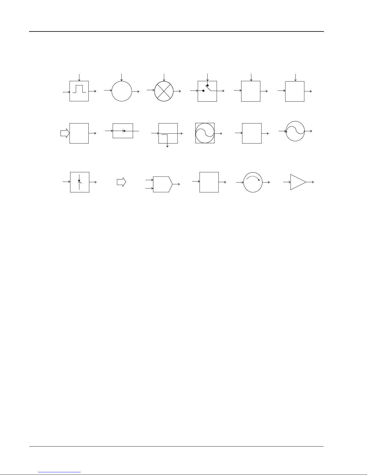
SYMBOLS
Block diagram symbols frequently used in the manual are illustrated below.
Course
MOD
Pulse
Modulator
DAC
Digital to
Analog
Converter
Step-Recovery
Diode Multiplier
Fine
YIG-Tuned
Oscillator
RF Level
Detector
Digital
YIG
Data
Mixer
Coupler
V
R
Phase Lock
Loop
Switch
Fixed
Reference
Oscillator
DIV
N
Freque ncy
Divider
STEP
ATTEN
Step
Attenuator
LOW
PASS
Filter
Isolator
LVL
PIN-Diode
Leveler
Voltage-
Controlled
Oscillator
Amplifier
xiv
Manual No. 120AM00250, Rev C, September 1998

Record of Manual Changes
This table is provided for your convenience to maintain a permanent record of manual change d ata.
Corrected replacement pages will be issued as Technical Publication Change Instruction s, and will
be inserted at the front of the binder. Rem ove the corresponding old pages, insert the new pages,
and record the changes here.
Change Instruction
Number
Change Instruction
Date
Date
Entered Comments
Manual No. 120AM00250, Rev C, September 1998
xv

Series GT 9000 Microwave Synthesizers
xvi
Manual No. 120AM00250, Rev C, September 1998

Special Configurations
When the accompanying product has been configured for user-specific application(s), supplemental
pages will be inserted at the front of the manual binder. Remove this page and replace it with the
furnished Special Configuration supplemental page(s).
Manual No. 120AM00250, Rev C, September 1998
xvii

Series GT 9000 Microwave Synthesizers
xviii
Manual No. 120AM00250, Rev C, September 1998

1.1 General Information
1.1.1 Introduction
The Model GT 9000 Mi crowave Synthesizer provides si gnal generati on over a range of
synthesized microwave frequencies and power levels. It is capable of generating output signals
from 10 MHz to 26.5 GHz (the frequency range is dependent on the model). The RF output can
be modulated in AM, FM, and PM modes.
The following are the GT 9000 model numbers and frequency ranges:
GT 9000/.01 - 20 10 MHz to 20 GHz
•
GT 9000/.5 - 20 500 MHz to 20 GHz
•
GT 9000/2 - 20 2 GHz to 20 GHz
•
1
Introduction
GT 9000/.01 - 26 10 MHz to 26.5 GHz
•
GT 9000/.5 - 26 500 MHz to 26.5 GHz
•
GT 9000/2 - 26 2 GHz to 26.5 GHz
•
The Model GT 9000 generates output signals under manual control from the front panel, or
under remote computer control through the I EEE-488 General Purpose Interface Bus (GPIB).
Complete performance specifications are described later in this chapter.
The GT 9000 has a nominal weight of 43 lbs. It measures 5.25 inches high by 16.75 inches
wide by 24 inches deep. Power requirements are 100/120/220/240 VAC
250 Watt s nominal. See Section 1.2 fo r details on how to set the volt age and install t he correct
fuse for the are a in which the inst rument will be used .
The GT 9000 is type tested to MIL-T-28800E, Type III, Class 5, Style E, except as follows:
Operating temperature range is 0 to 50° Celsius.
•
Warm-up time is 20 minutes for normal operation (for warm-up time prior to calibration and
•
testing, see Chapter 4).
Storage temperature is -40° C to +70°C.
•
Relative humidity is limited to 95% non-condensing.
•
Altitude and EMI requirements are not specified.
•
+10%, 47-400 Hz,
Manual No. 120AM00250, Rev C, September 1998
1-1

Model GT 9000 Microwave Synthesizer
1.1.2 Items Furnished
In addition t o options and/or accessorie s specifically or dered, items fu rnished with the
instrument are as follows:
1 ea. - Operation and Maintenance Manual
1 ea. - 6 ft. power cord
2 ea. - PC Extender Board
1 ea. - PC Card Extractor
1.1.3 Items R e q u ired
An IEEE-488 interface cable is needed for remote control operation. Appropriate RF output
cabling to fit the f emale type SMA output connect or can be ordered as an Acces sory Cable Kit,
No. A001.
1.1.4 Tools and T est Equipment
No special tools ar e required to operate the GT 9000. Test equipment required for calibrat ion or
performance verification is described in Chapter 4.
1.1.5 Cooli ng
A cooling fan is installed in the instrument. The cooling air intake and exhaust are both located
on the rear pa nel. Care must be ta ken to avoid obstructin g the flow of air into a nd out of the
instrument.
1.1.6 Clean ing
The air inlet screen should be cleaned whenever a significant amount of dirt or dust has
accumulated. Whe never the covers are removed, the interio r should be blown out with dr y air at
a low velocity.
1.1.7 Installation and Preparation for Use
The GT 9000 is shipped in operational condition and no special installation procedures are
required. A warm-u p time of 20 minutes is re commended for normal op eration (for warm- up
time prior to calibration and testing, see Chapter 4) .
1.1.8 Receiving Inspection
Use care in removing the instrument from the carton and check immediately for physical
damage, such as bent or broken connectors on the front and rear panels, dents or scratches on
the panels, b roken extractor handles , etc. Check the shipping cart on for evidence of phys ical
damage and immedi ately report any damage to the shippi ng carrier.
When the instr ument is received, check th e carton for evidence o f damage. If dama ge is found,
notify the carrier immediately, and open the carton only in the carrier’s presence.
Each Giga-tronics instrument must pass rigorous inspections and tests prior to shipment. Upon
receipt, it should immediately be subjected to a performance check to ensure that operation has not
been impaired during shipment. The performance verification procedure is described in Chapter 4 of
this manual.
1-2
Manual No. 120AM00250, Rev C, September 1998

1.1.9 Preparation for Reshipment
To pr otect the inst rument during r eshipment, use the best packagi ng materials available. If
possible use the original shipping container. If this is not possible, a strong carton or a wooden
box should be us ed. Wrap the ins trument in heavy pape r or plastic befo re placing it in the
shipping contain er. Completely fill the areas on all si des of the instru ment with packaging
material. Take extra precautions to pro tect the fro nt and rear panels.
Seal the package with strong tape or metal bands. Mark the outside of the package “FRAGILE
— DELICATE INSTRUMENT”. If correspondin g with the factory or local Giga-t ronics sales
office regarding reshipme nt, please ref erence the ful l model number and s erial number. If the
instrument is being reshipped for repair, enclose all available pertinent data regarding the
problem that has been found.
Introduction
☛
If you are retur ning an in strumen t to Giga-troni cs for servi ce, first cont act
NOTE:
Giga-tronics Cu st omer Service a t
a retur n authorization number can be assigned. You can also contact Cus tomer
Service at
www.repairs@gigatronics.com
(800) 444 -2878
or Fax at
(925) 328-47 02
so that
Manual No. 120AM00250, Rev C, September 1998
1-3
Model GT 9000 Microwave Synthesizer
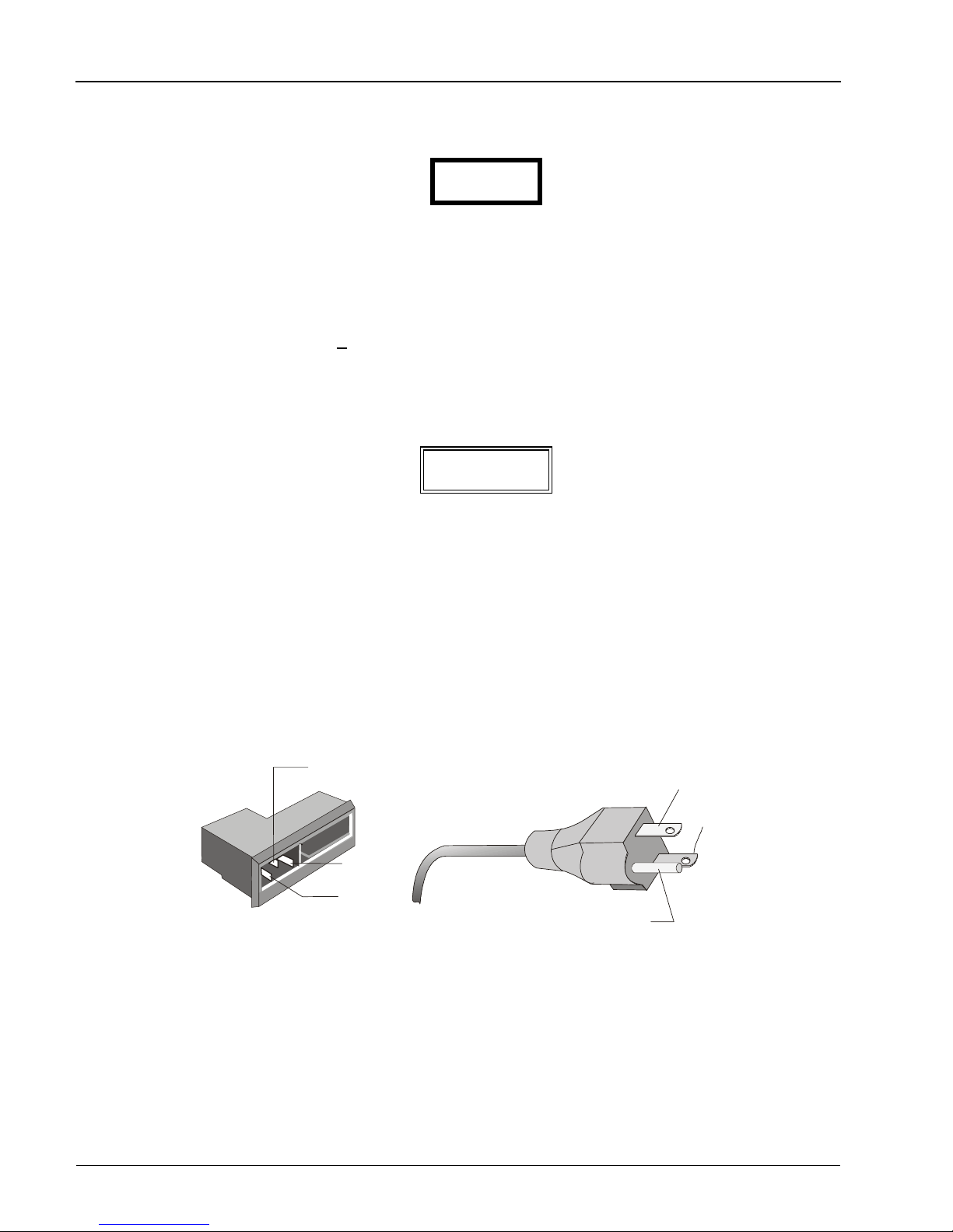
1.2 Safety Precautions
The instrument can be damaged if you attempt to operate it while the line voltage
selector and fuses are incorrect for the applied line voltage.
Before operatin g the instrument, make sure the voltage sele ction and fuses are compatible with
the power source to be used. The instrument has be en designed for in ternational voltages of
100, 120, 220, or 240 VAC,
connector that includes voltage selection, fuse and filter for RFI protection.
The GT 9000 has a 3-wire power cord with a 3-terminal polarized plug f or connection to the
power sour ce and safety ground.
+10%, at 50-400 H z. The GT 9000 uses an internationa lly approved
CAUTION
WARNING
The safety ground is connected directly to the chassis. If a 3-to-2 wire adapter is
to be used, be sure to connect the ground lead from the adapter to earth ground.
Failure to do this could cause the instrument to float above ground, posing a shock
hazard.
EARTH GRO U ND
LINE
NEUTRAL
LINE
NEUTRAL
EARTH GRO U ND
1-4
Figure 1-1. Power Line Connection
Manual No. 120AM00250, Rev C, September 1998
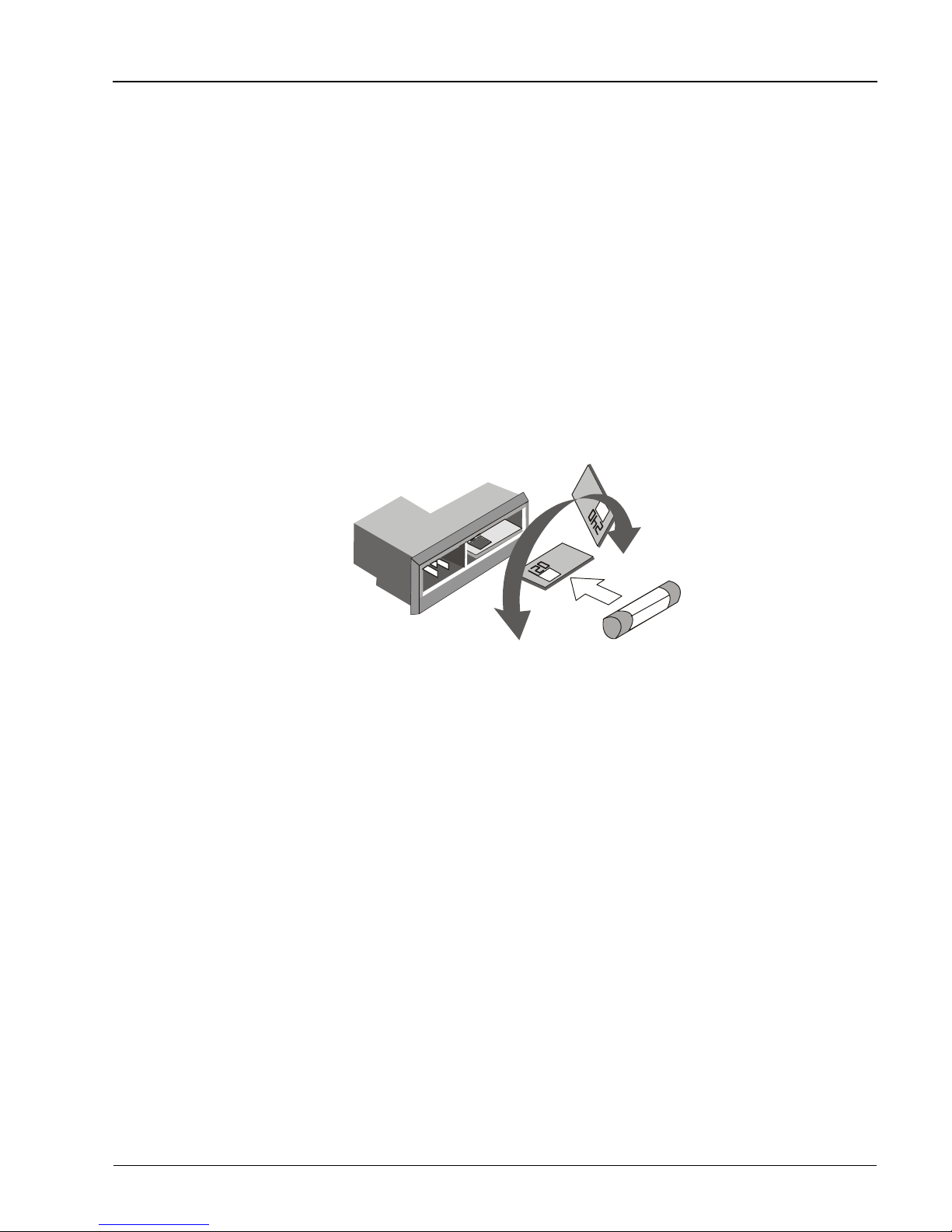
1.2.1 Voltage and Fuse Selection
When the GT 9000 is shi pped from the factor y, i t is set for a line voltage of 120 V for domestic
destinations. The power line fuse for this setting is a 4 A 3AG Slo-Blo. If the instrument is set
to operat e on a 240 V power line, the fuse must be change d to a 2 A 3AG Slo-Blo.
To se lect a different o perating li ne voltage and f use, proceed a s follows:
1. Open the cover door and rotate the fuse-pull to the left; remove the fuse.
2. Select the operating voltage by orienting the PC board so that the correct voltage label
is on the top left side.
3. Pu sh the board firmly in to the module slot .
4. Ro tate the fuse-pu ll back into the nor mal position an d reinsert the fu se into the holder,
using care to sele ct the correct fuse value.
Introduction
Operating voltage is shown
in the module window
Figure 1-2. Voltage Selector and Fuse Holder
Manual No. 120AM00250, Rev C, September 1998
1-5
Model GT 9000 Microwave Synthesizer
1.3 Performance Specifications
1.3.1 CW Ope ration
Range: From .01, .5, or 2 GHz to 26.5 GHz
(see the serial number tag)
Resolution: 1 kHz (1 Hz with Option 16)
Accuracy And Stability: Identical to time base oscillator.
Time Base (internal): 10 MHz
Aging Rate:
Temperature Stability:
Time Base (external):
Switching Time: <50 ms (20 ms, typical) to within specified frequency accuracy.
1.3.2 Spect r al Pur it y
Harmonics
(measured at +6 dBm): - 40 dBc, .01 to.1 GHz
Subharmonics: None
<1 × 10
(<5 × 10
×
<+2
5 or 10 MHz (+1 × 10
-50 dBc, >.1 to 2 GHz
-65 dBc, >2 to 26.5 GHz
-9
/day after 72 hours of continuous operation
-10
/day with Option 28).
-10
10
/° C (0 to +50° C).
-6
or better), user selectable from the front panel or via GPIB
Nonharmonics: <-55 dBc
Single-Sideband Phase Noise (dBc/Hz noise bandwidth, all power levels):
Freq.
250 MHz -87 -87 -85 -122 -135
500 MHz -97 -95 -95 -127 -135
2 GH z -90 -91 -90 -125 -130
6 GH z -80 -83 -81 -115 -130
10 G Hz -75 -80 -80 -1 05 -128
20 G Hz -72 -75 -75 -1 05 -120
23 GHz -65 -70 -70 -97 -108
2 GHz -83 -85 -84 -118 -130
100 Hz 1 kHz 10 kHz 100 kHz 1 MHz
For 2 - 20 and 2 - 26 GHz Instruments
Offset from Carrier
Residual FM: (Hz, RMS, CW mode)
Frequency
Range (GHz)
.01 to <.5 10 75
.5 to 2 5 25
>2 to <8
8 to <20 30 300
20 t o 2 6.5 40 40 0
1
1
Specification applies from 2 GHz for Models GT 9000/2 - 20 and GT9000/2 - 26
Post-detection Bandwidth
0.3 to 3 kHz 0.5 to 15 kHz
20 100
1-6
Manual No. 120AM00250, Rev C, September 1998

1.3.3 RF Output Power
Introduction
Maximum Leveled Output:
Frequency
Range (GHz)
.01 to 2 +13 +13
1
>2 to 8
8 to 15 +14 +13
>15 to <20 +13 +11
20 to 26. 5 +9.5 +7.5
1
Specification applies from 2 GHz for Models GT 9000/2 - 20 and GT9000/2 - 26
Standard
(dBm)
+15 +15
With Option 26
(dBm)
Incremental Level Range: - 20 to +20 dBm
Resolution: 0.01 dB, entry and display to -99.99 dBm (display is 0.1 dB at <-100.0 dBm).
Minimum Output Level: -10 dBm (-20 typical); -120 dBm with Option 26 (20 GHz), -100 dBm (26 GHz)
RF OFF: Typically attenuates a 0 dBm signal to <-140 dBm at the output connector.
Output Accuracy
(internally leveled, Scan/AM
off): <+2 dB (-10 dBm to maximum specified power).
Add
+.1 dB/10 dB with Option 26.
Output Flatness: <
+2 dB
Output Switching Time: Typica lly <1 ms; 20 ms with attenuator change (Option 26).
Output Impedance:
50 Ω, nominal.
Output SWR: <2:1
External Leveling: Output power may be externally leveled by positive or negative ZBS detectors or
power meters.
1.3.4 PM Envelope Paramete rs
Pulse/Square Wave Modulation (PM) s pecifications appl y with Scan/AM and FM off. PM may
be operated with FM.
On/Off Ratio: >80 dB
Rise/Fall Times: <10 ns
Overshoot, Undershoot
& Ringing: +2 dB, maximum
Settling Time (to within 1 dB): <100 ns
Leveled Pulsed Output Power
(referenced to leveled,
unmodulated
output power): +0.5 dB, typical (>100 ns pulse width);
+1 dB typical (<100 ns pulse width).
Manual No. 120AM00250, Rev C, September 1998
1-7

Model GT 9000 Microwave Synthesizer
1.3.5 Internally Generated PM Repetition Rate
Repetition Rate:
1 Hz to 100 Hz 1 Hz
100 Hz to 1 kHz 1 Hz
1 kHz to 10 kH z 10 Hz
10 kHz to 100 kHz 100 Hz
10 kHz to 1 MH z 1 kHz
1 MHz to 3 MHz 10 kHz
Accuracy: +0.02% of range maximum value.
Jitter: Same as instrument time base.
1.3.6 Internally Generated PM Delay
(referenced to Sync Output)
Range: 0 to 2 s
Resolution: 10 ns
Accuracy:
Jitter: 0.01% of setting or 100 ps, whichever is greater.
+1% of setting or 20 ns, whichever is greater.
1.3.7 Internally Generated PM Width
Range: 50 ns to 2 s
Range Resolution
Resolution: 10 ns
Accuracy:
Jitter: 0.01% of setting or 100 ps, whichever is greater.
+1% of setting or 20 ns, whichever is greater.
1.3.8 Externally T rig gered PM En velope
(one envelope produced by each trigger s upplied)
Repetition Rate: 5 Hz to 5 MHz
Pulse Delay: Set by internal delay control.
Pulse Width: Set by internal width control.
Input Trigger Required: Positive or negative-going TTL level trigger pulse, >25 ns wide.
1.3.9 E xternally Generated PM Envelope
(one envelope produced by each pulse sup plied)
Repetition Rate: 5 Hz to 5 MHz, leveled output;
DC to 10 MHz, unleveled output.
Pulse Delay (output enve lope
leading edge referenced to
input pulse leading edge): 50 ns, typical
Input Pulse Required: Positive or negative-going TTL level pulse,
>50 ns wide (leveled output);
>20 ns wide (unleveled output).
1-8
Manual No. 120AM00250, Rev C, September 1998

1.3.10 FM Envelope Parameters (Wide or Narrow Mode)
Introduction
☛
Modulation Accuracy:
Frequency Modulation (FM) specifications apply with Scan/AM and PM off.
NOTE:
FM may be operated simultaneously with AM or PM.
Distortion: <5%
Incidental AM: <
+0.2%/MHz of deviation
+5%, at maximum deviation and a 1 kHz rate.
1.3.11 FM Envelope Parameters (Wide Mode)
Max Deviation: 2.5 MHz peak (<2 GHz);
10 MHz peak (>2 GHz).
For 2-26 GHz instruments: 10 MHz peak (>2 GHz).
Flatness:
Residual FM (50 Hz to 15 kHz
post-detection bandwidth): <750 Hz, typical (<2 GHz);
+2 dB for rates from 10 Hz to 1 MHz;
+3 dB for rates from 1 to 5 MHz.
<3 kHz rms, typical (>2 GHz).
For 2-26 GHz instruments: <3 kHz rms, typical (>2 GHz).
1.3.12 FM Envelope Parameters (Narrow Mode)
Max Deviation:
Flatness:
Residual FM: The same as for an unmodulated RF output (see
The lesser of 25
the lesser of 100
For 2-26 GHz instruments: the lesser of 100 x F
+2 dB for rates from 20 kHz to 1 MHz;
+3 dB for rates from 1 to 5 MHz.
Spectral Purity).
×
×
F
mod
F
mod
or 2.5 MHz, peak (<2 GHz);
or 10 MHz, peak (>2 GHz).
mod
or 10 MHz, peak (>2 GHz).
1.3.13 FM Indicator
Readout: 6 digits; displays deviation (also displays rate, if
1.3.14 Internally Generated FM Envelope (Option 24 only)
Waveform: Sine, square, or triangle wave.
Resolution: 1 Hz
Accuracy:
Manual No. 120AM00250, Rev C, September 1998
Option 24 is installed).
Rate: 10 Hz to 1 MHz
+0.01 Hz
1-9
Model GT 9000 Microwave Synthesizer
1.3.15 Externally Supplied FM Envelope
Waveform: Any waveform compatible with bandwidth considerations.
Rate: 10 Hz to 5 MHz
Sensitivity: Settable; calibrated for 1 Vp input.
RF Output
Frequency
<2 GHz 2.5 MHz 0 to 2.5 MHz 625 Hz
>2 GHz 10 MHz 0 to 10 MHz 2.5 kHz
>
2 GHz 10 MHz 0 to 10 MHz 2.5 kHz
External FM Sensitivity
Deviation at
1 Vp in
For 2-26 GHz instruments:
Deviation
Range
Deviation
Increments
Input Impedance:
50 Ω, nominal
1.3.16 Amplitude Modulation
☛
NOTE:
Option 27; see Appendix A for option information. AM may be operated
simultaneously with FM.
Modulation Depth: 0 to 90%, typical, at 0 dBm out
Modulation Bandwidth: DC to 30 kHz,
Modulation Accuracy: Set depth +10% depth (e.g., the depth at a 50% setting may be 40 to 60%).
The AM specifications given here do not apply to instruments with
1.3.17 AM Indicator
Depth Readout: 4 digits; 0.1% depth resolution
Rate Readout
(Option 24 only): 6 digits; 1 Hz rate resolution
1.3.18 Internally Generated AM Envelope
(Option 24 o nly)
+3 dB, typical, at 0 dBm out
Waveform: Sine, square, or triangle wave.
Rate: 1 Hz to 100 kHz
Resolution: 1 Hz
Accuracy:
1-10
+0.01 Hz
Manual No. 120AM00250, Rev C, September 1998
 Loading...