

Page 1

Manual Part Number:
Revision:
Print Date:
21568
F
March 2008
Series 8035XA Peak Power Sensors
Operation & Maintenance Manual
8035XA
............................................Certified Product
Registrar: BSI, Certification No. FM 34226 v Registered 04 June 1996 v Amended 01 March 2000
Giga-tronics Incorporated v 4650 Norris Canyon Road v San Ramon, California 94583
925.328.4650 or 800.726.4442 v 925.328.4700 (Fax) v 800.444.2878 (Customer Service) v 925.328.4702 (CS Fax)
www.gigatronics.com
ISO 9001.................................................. Certified Process
Page 2

All technical data and specifications in this manual are subject to change without prior notice and do not represe nt a
commitment on the part of Giga-tronics Incorporated.
© 2001 Giga-tronics Incorporated. All rights reserved.
Printed in the USA
WARRANTY
Giga-tronics Series 8035XA Peak Power Sensors
are warranted against defective materials and
workmanship for one years from date of shipment .
Giga-tronics will at its option repair or replace
products that are proven defective during the
warranty period. This warranty DOES NOT cover
damage resulting from improper use, nor
workmanship other than Giga-tronics service.
There is no implied warranty of fitness for a
particular purpose, nor is Giga-tronics liable f or any
consequential damages. Specification and price
change privileges are reserved by Giga-tronics.
Page 3

Declaration of Conformity
Application of Council Directive(s)
Standard(s) to which Conformity is Declared:
89/336/EEC and 73/23/EEC EMC Directive and Low Voltage Directive
EN61010-1 (1993) Electrical Safety
EN61326-1 (1997) EMC - Emissions & Immunity
Manufacturer’s Name: Manufacturer’s Address:
Giga-tronics, Incorporated 4650 Norris Canyon Road
San Ramon, California 94583
U.S.A.
Type of Equipment: Model Series Number:
Peak Power Sensors 8035XA
Model Numbers In Series:
80350A, 80351A, 80352A,
80353A, 80354A, 80355A
Declaration of Conformity on file. Contact Giga-tronics, Inc.
4650 Norris Canyon Rd.
San Ramon, CA 94583
Ph: 1-925-328-4650
Fx: 1-925-328-4700
Page 4

Page 5

1
Introduction
2
Operation
Table of Contents
About This Manual .................................................................................................. 1-vii
Conventions ........................................................................................................... 1-viii
Record of Manual Changes ........................................................................................1-x
Special Configurations ..............................................................................................1-xi
1.1 Description....................................................................................................1-1
1.1.1 Accessories ..................................................................................1-1
1.1.2 Product Returns ...........................................................................1-1
1.2 Specifications ...............................................................................................1-2
1.2.1 Performance Specifications ...........................................................1-3
1.2.2 Compatible Power Meters ............................................................1-5
3
2.1 Introduction ..................................................................................................2-1
2.2 Power Sweep Calibration ..............................................................................2-1
2.2.1 5, 25 and 50 Watt Peak Power Sensors ........................................2-2
2.2.2 Triggering .....................................................................................2-3
2.2.3 Zeroing .........................................................................................2-4
2.2.4 Sensor Triggering .........................................................................2-5
2.3 Sample Delay ................................................................................................2-6
2.3.1 Sample Delay Display ...................................................................2-7
2.3.2 Setting Sample Delay ...................................................................2-8
2.3.3 Sample Delay Limits .....................................................................2-9
2.3.4 Setting Sample Delay Offset .......................................................2-10
2.3.5 Single Peak Sample Measurements ............................................2-10
2.3.6 Real Time Pulse Profile and Sample Position Display ..................2-11
2.3.7 Sample Delay Offset ...................................................................2-12
2.3.8 Measuring Pulse Droop ..............................................................2-13
2.3.9 Measuring 3 dB Pulse Width ......................................................2-14
2.3.10 Measuring Rise-Time ..................................................................2-15
2.4 GPIB Commands.........................................................................................2-15
2.4.1 Setting Trigger Modes ................................................................2-15
2.4.2 Setting Delays ............................................................................2-16
2.4.3 Reading Values ...........................................................................2-17
2.4.4 Commands for the 58542 ...........................................................2-18
Theory of Operation
Manual 21568, Rev. F, March 2008 i
Page 6

Series 8035XA Peak Power Sensors
3.1 Introduction...................................................................................................3-1
3.2 Analog Assembly Description........................................................................3-2
3.3 Digital Assembly Description.........................................................................3-5
3.3.1 Overview ......................................................................................3-5
3.3.2 Description ...................................................................................3-6
Calibration and Testing
4.1 Introduction...................................................................................................4-1
4.2 Equipment Required......................................................................................4-1
4
4.3 Power Linearity Test......................................................................................4-2
4.3.1 CW Linearity Test .........................................................................4-2
4.3.2 Peak Linearity Test ........................................................................4-3
4.4 Trigger Modes Tests .....................................................................................4-4
4.4.1 Detector Output Test ....................................................................4-4
4.4.2 Trigger Level Test .........................................................................4-4
4.4.3 Delay Test ....................................................................................4-6
4.4.2.1 100 mW Power Peak Sensors..................................... 4-4
4.4.2.2 High Power Peak Sensors........................................... 4-5
Maintenance
5
6
Parts Lists
5.1 Introduction...................................................................................................5-1
5.1.1 Rise-Time Adjustments .................................................................5-1
5.1.2 Zero Adjustment ...........................................................................5-2
5.2 Troubleshooting ............................................................................................5-2
5.2.1 Sensor Not Present .......................................................................5-4
5.2.2 Calibration ....................................................................................5-4
5.2.3 INTernal ........................................................................................5-5
5.2.4 EXTernal .......................................................................................5-6
5.2.5 Delay ............................................................................................5-6
5.2.6 Output Problems ..........................................................................5-6
5.3 Sensor Element Replacement ........................................................................5-7
5.3.1 Disassembly of the Sensor ...........................................................5-7
5.3.2 Replacing the Sensor Element ......................................................5-7
5.3.3 Reassembly of the Sensor ............................................................5-8
6.1 Introduction...................................................................................................6-1
80350A PEAK POWER SENSOR, TYPE N, Rev. F....................................... 6-1
80351A HI PWR PEAK POWER SENSOR, 5W, Rev. C................................ 6-2
80352A HI PWR PEAK POWER SENSOR, 25W, Rev. C.............................. 6-3
80353A PEAK POWER SENSOR, TYPE K, Rev. D....................................... 6-4
80354A PEAK POWER SENSOR, TYPE K, Rev. E....................................... 6-5
80355A HI PWR PEAK POWER SENSOR, 50W, Rev. C.............................. 6-6
32133 SENSOR-S-CLOCK-BUFFER PCA, Rev. A...................................... 6-6
21471 SENSOR HOUSING ASSY, Rev. C................................................. 6-7
ii Manual 21568, Rev. F, March 2008
Page 7

7
Diagrams
Index
Preface
21350 ANALOG PCB ASSY (A1), Rev. P.................................................. 6-8
21353 DIGITAL PCB ASSY (A2), Rev. Z................................................. 6-10
6.2 List of Manufacturers..................................................................................6-12
7.1 Introduction ..................................................................................................7-1
Series 8035XA Peak Power Sensors Index........................................................... Index-1
Manual 21568, Rev. F, March 2008 iii
Page 8

Series 8035XA Peak Power Sensors
Illustrations
Figure 2-1: Sensor Setup Menu Tree ......................................................................2-2
Figure 2-2: Internal Triggering Levels......................................................................2-3
Figure 2-3: 8035XA Sensor Timing Diagram...........................................................2-4
Figure 2-4: Sample Delay Adjustment Display ........................................................2-6
Figure 2-5: Channel A Default Sample Delay ..........................................................2-7
Figure 2-6: Channel B Default Sample Delay...........................................................2-7
Figure 2-7: Channel A & B Default Sample Delay....................................................2-7
Figure 2-8: Sample Delay with Uncalibrated Sensor ...............................................2-7
Figure 2-9: Sample Delay with No Trigger Display..................................................2-9
Figure 2-10: Sample Dely Over-Range Indication......................................................2-9
Figure 2-11: Sample Delay Over-Range Offset Display............................................2-10
Figure 2-12: Pulse Profile and Sample Delay Test Setup.........................................2-11
Figure 2-13: Sample Delay......................................................................................2-12
Figure 2-14: Using SD to Offset a 0 ns Time Reference...........................................2-12
Figure 2-15: SD Setting for Measuring Pulse Droop................................................2-13
Figure 2-16: Using SD to Measure a 3 dB Pulse Width...........................................2-14
Figure 3-1: 8035XA High Level Block Diagram........................................................3-2
Figure 3-2: Analog PC Assembly Block Diagram.....................................................3-3
Figure 3-3: Analog Circuit Timing Diagram.............................................................3-4
Figure 3-4: Digital PC Assembly Block Diagram......................................................3-5
Figure 3-5: Digital Timing Diagram, INT/EXT Trig Mode..........................................3-7
Figure 3-6: Digital Timing Diagram, CW Mode .......................................................3-8
Figure 3-7: Digital Serial Data Cycle Timing Diagram..............................................3-8
Figure 4-8: Power Linearity Test Setup...................................................................4-2
Figure 4-9: Detector Output and Trigger Level Setup..............................................4-4
Figure 5-10: Principal Test Component Locations.....................................................5-2
iv Manual 21568, Rev. F March 2008
Page 9

Tables
Preface
Table 1-1: Peak Power Sensor Selection Guide..................................................... 1-2
Table 1-2: Power Sensor Cal Factor Uncertainties ................................................ 1-5
Table 6: Sample Delay Limits ............................................................................ 4-6
Table 7: 80350A, 80353A, 80354A Trigger Test............................................... 4-9
Table 8: 80351A Trigger Test............................................................................ 4-9
Table 9: 80352A, 80355A Trigger Verification................................................... 4-9
Table 10: External Trigger Verification................................................................. 4-9
Table 11: Sample Delay Test............................................................................. 4-10
Table 5-1: Sensor Malfunction Symptoms............................................................ 5-3
Table 5-2: Digital Board Components and Signals................................................ 5-6
Table 6-1: List of Manufacturers ........................................................................ 6-12
Manual 21568, Rev. F, March 2008
Page 10

Series 8035XA Peak Power Sensors
vi Manual 21568, Rev. F, March 2008
Page 11

About This Manual
This manual contains the following chapters and appendices to describe the operation and
maintenance of Giga-tronics Series 8035XA Peak Power Sensors:
Preface:
In addition to a comprehensive Table of Contents and general information abou t the manual,
the Preface also contains a record of changes made to the manual since its publication, an d
a description of Special Configurations. If you have ordered a user-specific manual, please
refer to page
Chapter 1 – Introduction:
This chapter contains a brief introduction to the instrument and its performance parameters.
Chapter 2 – Operation:
This chapter is a guide to operating the sensor with the Series 8540X Universal Power
Meters and the Model 58542 VXIbus Universal Power Meters.
Chapter 3 – Theory of Operation:
xi for a description of the special configuration.
This chapter provides a block diagram level description and its circuits for maintenance and
applications.
Chapter 4 – Calibration & Testing:
Procedures for inspection, calibration and performance testing are outlined in this chapter.
Chapter 5 – Maintenance:
This chapter contains procedures for main te na nce and troubleshooting.
Chapter 6 – Parts Lists:
This chapter lists all components and parts and their sources.
Chapter 7 – Diagrams:
This chapter contains schematics and parts placement diagrams for all circuits.
Index:
A comprehensive word index of the various elements of the 8035XA manual.
Changes that occur after publication of the manual, and Special Configuration data will be
inserted as loose pages in the manual binder. Please insert and/or replace the indicated
pages as detailed in the Technical Publication Change Instructions included with new and
replacement pages.
Manual 21568, Rev. F, March 2008
Page 12

Series 8035XA Peak Power Sensors
The following conventions are used in this product manual. Additional conventions not included
here will be defined at the time of usage.
Warning
The WARNING statement is encased in gray and centered in the
page. This calls attention to a situation, or an operating or
maintenance procedure, or practice, which if not strictly corrected
or observed, could result in injury or death of personnel. An
example is the proximity of high voltage.
Caution
Conventions
WARNING
CAUTION
The CAUTION statement is enclosed with s ingle lines and c entered
in the page. This calls attention to a situation, or an ope rating or
maintenance procedure, or practice, which if not strictly corrected
or observed, could result in temporary or permanent da mage to the
equipment, or loss of effectiveness.
Notes
*
Logic Not
A logic NOT or LOW condition used in text will be indicated by an overscore, such as LOADCTR. Elsewhere, such as in schematics, a logic NOT or LOW condition may be indicate d by a
forward slash bar, such as /LOAD-CTR.
Key Press Commands
Commands requiring specific keys to be pressed on the supporting device, such as power
meter, are indicated by square brackets. For example, [ENTER] means to press the Enter Key.
NOTE: A NOTE Highlights or amplifies an essential operating or maintenance procedure,
practice, condition or statement.
viii Manual 21568, Rev. F, March 2008
Page 13

Manual 21568, Rev. F, March 2008
Page 14

Series 8035XA Peak Power Sensors
This table is provided for your convenience to maintain a permanent record of manual change
data. Corrected replacement pages will be issued as Technical Publication Change
Instructions, and will be inserted at the front of the binder. Remove the corresponding old
pages, insert the new pages, and record the changes here.
Record of Manual Changes
Change Instruction
Number
Change Instruction
Date
Date
Entered
Comments
x Manual 21568, Rev. F, March 2008
Page 15

Special Configurations
When the accompanying product has been configured for user-specific applicatio n(s),
supplemental pages will be inserted at the front of the manual binder. Remove the indicated
page(s) and replace it (them) with the furnished Special Configuration supplemental page(s).
Manual 21568, Rev. F, March 2008
Page 16

Series 8035XA Peak Power Sensors
xii Manual 21568, Rev. F, March 2008
Page 17

Manual 21568, Rev. F, March 2008
Page 18

Series 8035XA Peak Power Sensors
xiv Manual 21568, Rev. F, March 2008
Page 19

1.1 Description
The 8035XA Series Peak Power Sensors perform true sample-based peak power
measurements on pulsed signals. The sensors are compatible with Giga-tronics Series 8540,
and the 8650 series Universal Power Meters and the Model 58542 VXIbus Universal Power
Meter (see Section
power versions of 5, 25 and 50 Watts, are available to 18 GHz. (see Table 1-1).
Peak Power sensors have three modes of operation: (1) CW, (2) Peak, internally triggered , and
(3)
Peak, externally triggered. When operated in the pea k mode s, trigge r- point to sam ple- point
delay (sample delay) is adjustable from -20 ns to 100 ms in 0.5 ns steps. T rigger levels are also
adjustable.
The Giga-tronics proprietary power sweep calibration system provides excellent linearity from
-20 dBm to +20 dBm in Peak modes, and from -30 dBm to +20 dBm in CW mode. Cal Factors
stored in EEPROMs in the power sensors automatically compensate for sensor frequency
response variations. This unique approach can be configured for automatic frequency
response correction. A detector output signal is provided for viewing the detected envelope of
the pulsed RF waveform on an oscilloscope. Use of a digital oscilloscope is recommended.
1
Introduction
1.2.2). The sensors operate from 45 MHz to 18, 26.5, and 40 GHz. High
1.1.1 Accessories
Included: 3 each SMB (plug) to BNC (m) cables, 2 m (6 ft) long
Optional: Option 02: 12 ft SMB (plug) to BNC cable
1.1.2 Product Returns
Should it be necessary to return the product to Giga-tronics, use the original shipping container.
If this is not possible, use a strong carton (350 lbs/in
Wrap the instrument in heavy paper or plastic before placing it in the shipping container.
Completely fill the areas on all sides of the instrument with packaging material, taking extra
precautions to protect the front and rear panels. Seal the package with strong tape or metal
bands. Mark the outside of the package “FRAGILE — DELICATE INSTRUMENT”.
If corresponding with the factory or the local Giga-tronics sales office regarding a product
return, please refer to the full model number and serial number. If the instrument is being
3 each Cable Harness Wraps, 1.2 m (4 ft) long
Option 03: SMB (plug) to SMA (jack) adapter
2
bursting strength), or a wooden box.
Manual 21568, Rev. F, March 2008
Page 20

Series 8035XA Peak Power Sensors
*
shipped for repair, be sure to enclose all available pertinent data regar ding the problem that
has been found.
NOTE: If you are returning an instrument to Giga-tronics for service, first contact Customer
Service so that a return authorization number (RMA) can be assigned via e-mail at
repairs@gigatronics.com or at 800.227-9764 (The 800 number is only valid within the US).
You may also try our domestic line at 925.328.4650 or Fax at 925.328.4702.
1.2 Specifications
Table 1-1: Peak Power Sensor Selection Guide
Model
80350A
80353A
80354A
80351A
80352A
Freq. Range/
Power Range
45 MHz to 18 GHz
-20 to +20 dBm, Peak
-30 to +20 dBm, CW
45 MHz to 26.5 GHz
-20 to +20 dBm, Peak
-30 to +20 dBm, CW
45 MHz to 40 GHz
-20 to +0.0 dBm, Peak
-30 to +0.0 dBm, CW
45 MHz to 18 GHz
0.0 to +40 dBm, Peak
-10 to +37 dBm, CW
45 MHz to 18 GHz
+10 to +50 dBm, Peak
0.0 to +44 dBm, CW
Max.
Power
+23 dBm
(200 mW)
CW or Peak
CW:
+37 dBm
(5 W Avg.)
Peak:
+43 dBm
CW:
+44 dBm
(25 W Avg.)
Peak:
dBm
+53
Power Linearity
Standard Peak Power Sensors
-30 to -20 dBm ±0.00 dB
-20 to +20 dBm ±0.05 dB/10 dB
-30 to -20 dBm ±0.00 dB
-20 to +20 dBm ±0.1 dB/10 dB
-30 to -20 dBm ±0.00 dB
-20 to 0.0 dBm ±0.2 dB/10dB
-10 to +0 dBm ±0.00 dB
+0 to +40 dBm ±0.05 dB/10 dB
0.0 to +10 dBm ±0.00 dB
+10 to +50 dBm ±0.05 dB/10 dB
4
5W Peak Power Sensor
25W Peak Power Sensor
50W Peak Power Sensor
Type
N(m)
50Ω
Type
K(m)
50Ω
2,5
Type
N(m)
50Ω
3,5
Type
N(m)
50Ω
3,5
RF
Conn
1
Dimensions
Ln. Dia.
165 mm
(6.5 in)
200 mm
(7.9 in)
229.6mm
(9.05 in)
37 mm
1.25 in)
37 mm
(1.25 in)
41.15
mm
(1.62 in)
Wgt VSWR
1.12:0.045 - 2 GHz
1.22:2 - 12.4 GHz
1.37:12.4 -18 GHz
1.12:0.045 - 2 GHz
1.22:2 - 12.4 GHz
0.3 kg
1.37:12.4 -18 GHz
(0.7 lb)
1.50:18 - 26.5 GHz
1.12:0.045 - 2 GHz
1.22:2 - 12.4 GHz
1.37:12.4 -18 GHz
1.50:18 - 26.5 GHz
1.92:26.5 - 40 GHz
1.15:0.045 - 4 GHz
0.4 kg
1.25:4 - 12.4 GHz
(0.9 lb)
1.35:12.4 -18 GHz
1.20:0.045 - 6 GHz
0.4 kg
1.30:6 - 12.4 GHz
(0.9 lb)
1.40:12.4 -18 GHz
CW:
+47 dBm
(50 W Avg.)
Peak:
+53 dBm
0.0 to +10 dBm ±0.00 dB
+10 to +50 dBm ±0.05 dB/10 dB
Type
N(m)
50Ω
287.7
mm
(11.35 in)
41.15
mm
(1.62 in)
0.9 kg
(1.1 lb)
1.25:0.045 - 6 GHz
1.35:6 - 12.4 GHz
1.45:12.4 -18 GHz
80355A
45 MHz to 18 GHz
+10 to +50 dBm, Peak
0.0 to +47 dBm, CW
Notes:
1. The K connector is electrically and mechanically compatible with the APC-3.5 and SMA connectors.
2. Power coefficient equals <0.01 dB/Watt (AVG).
3. Power coefficient equals <0.015 dB/Watt (AVG).
4. For frequencies above 8 GHz, add power linearity to system linearity.
5. Peak operating range above CW maximum range is limited to <10% duty cycle.
1-2 Manual 21568, Rev. F, March 2008
Page 21

1.2.1 Performance Specifications
Performance specifications describe warranted performance. Typical performance shown in
italics is non-warranted. Specifications are subject to change without notice.
Rise-Time (10% to 90%, 0 dBm = 100%) < 100 ns
Fall Time (90% to 10%, 0 dBm = 100%) < 250 ns
System Linearity (50 MHz for Standard Peak Power Sensors:)
±0.13 dB from -30 to +16 dBm
±0.13 dB +(+0 dB, -0.05 dB/dB) from +16 to +20 dBm
Manual 21568, Rev. F, March 2008
Page 22

Series 8035XA Peak Power Sensors
Zero Accuracy
Applies to 80350A, 80353A and 80354; 80351A = 100x larger,
80352A = 1000x larger
Zero Set: < ±1.0 mW, Peak;
Zero Drift: < ±1.0 mW, Peak
Noise Uncertainty: < ±1.0 mW, Peak;
Sample Delay Timing
Delay Range: -20 ns to 104 ms
Delay Resolution: 0.5 ns
Delay Jitter: ±2.0 ns
Trigger Level Set Range:
Internal: -30 to +20 dBm
Resolution: ±0.01 dB
External: 0.0V to 4.0V
Trigger Jitter: < ±2.0 ns
Settling Time: (50% to within 3%) < 250 ns
Control Inputs and Outputs
< ±0.05 mW, CW
< ±0.05 mW, CW
in 1 hour at constant temperature, 24 hour warmup
< ±0.05 mW, CW at constant temperature, measured over a 1
minute interval, 24 hour warmup
Resolution to 0.01V
Trigger Input: [SMB (jack) connector]
Detector Out: [SMB (jack) connector]
Sample Delay: [SMB (jack) connector]
TTL External Trigger Input (absolute maximum = 10 V)
110 kΩ Impedance.
Monitor real time pulse waveform on an oscilloscope with this
voltage output (uncalibrated)
(High Impedance - Do Not Terminate)
High, 5 V, between trigger and sample points. Connect to digital
oscilloscope channel 2 for triggering and sample point
identification
(High Impedance - Do Not Terminate)
Maximum cable length = 3 meters
1-4 Manual 21568, Rev. F, March 2008
Page 23

Table 1-2: Power Sensor Cal Factor Uncertainties
Freq. (GHz) Sum of Uncertainties (%)
Lower Upper 8035XA
0.1 1 1.61 3.06 9.09 9.51 10.16 1.04 1.64 4.92
1 2 1.95 3.51 9.43 9.85 10.50 1.20 1.73 5.04
2 4 2.44 4.42 13.10 13.57 14.52 1.33 1.93 7.09
4 6 2.67 4.74 13.33 13.80 14.75 1.41 2.03 7.17
6 8 2.86 4.94 13.52 13.99 14.94 1.52 2.08 7.25
8 12.4 3.59 6.04 14.25 14.72 15.67 1.92 2.55 7.56
12.4 18 4.09 6.86 19.52 20.97 21.94 2.11 2.83 12.37
18 26.5 —— 9.27 —— —— —— —— 3.63 ——
26.5 40 —— 15.19 —— —— —— —— 6.05 ——
80353A
80354A
80351A
3
1
80352A
Probable Uncertainties (%)
3
80355A
3
8035XA
80353A
80354A
80351A
80352A
80355A
Notes:
1. Includes uncertainty of reference standard and transfer uncertainty. Directly traceable to NIST.
2. Square root of sum of the individual uncertainties squared (RSS).
3. Cal Factor numbers allow for 3% repeatability when connecting attenuator to sensor, and 3% for attenuator
measurement uncertainty and mismatch of sensor/pad combination. Attenuator frequency response is added to
the Sensor Cal Factors which are stored in the sensor’s EEPROM.
2
3
3
3
1.2.2 Compatible Power Meters
8541X Single Channel Universal Power Meter
8542X Dual Channel Universal Power Meter
8651A Single Channel Universal Power Meter
8652A Dual Channel Universal Power Meter
58542 Dual Channel VXI Universal Power Meter
NOTE: If the Series 8035XA sensors will be used with a Model 8542 (dual channel) Power
Meter, the 8542 must be configured to code 06 or higher, or an asterisk (*) must be appended
to the code number. The code number is printed next to the serial number on the label
located on the rear panel of the 8542.
Manual 21568, Rev. F, March 2008
Page 24

Series 8035XA Peak Power Sensors
1-6 Manual 21568, Rev. F, March 2008
Page 25

2.1 Introduction
When a sensor is first connected to a Model 8540 or 8650 Series Unive rsal Power Meter or to a
Model 58542 VXIbus Universal Power Meter, it is necessary to calibrate the sensor to the
meter’s sensor input, using the meter’s power sweep calibration system. The power meter will
not allow measurements to be performed until this calibration is completed successfully. It is a
good practice to repeat the calibration whenever the ambient operating temperature of the
sensor varies by more than ±5 °C (±9 °F), and whenever any external connections or external
loads are added or removed from the sensor. Always a llow a 30 minute warm-up perio d before
calibrating the sensor.
2
Operation
*
The operational description of the 8035XA Peak Power Sensor applies to applications with
either the Series 8540 or 8650 Universal Power Meters (8541 /2, B and C) or the Model 58542
VXIbus Universal Power Meter. Except where noted, the front panel descriptions apply only to
the Series 8540 Power Meters, and SCPI command sequences apply to the Model 58542
VXIbus Power Meter. The Series 8650 Power Meter display lines vary from the Series 8540 but
include the same parameters.
NOTE: These instructions show the Series 8540 Power Meter front panel keys in brackets
[ ] and menu displays in bold print.
2.2 Power Sweep Calibration
Procedures for calibrating sensors to the meter are detailed in the specific power meter
manual. The 8035XA Peak Power Sensors are calibrated to the meter using the same
procedure as other sensors used with the 8540, 8650 Series Power Meters or the 5854 2 VXI
Power Meter. Connect the channel A sensor to the calibrator port, and press [ZERO/CAL].
Following the successful completion of Power Sweep Calibration, the 8541/2 will automatically
display the current value of sample delay for your 8035XA Series Peak Power Sensor. If the
sample delay does not appear, press [RECALL], select PRESET, and press [ENTER].
If you are using the dual channel 8542 Universal Power Meter, verify that only one 8035XA
Series Peak Power Sensor is connected. The 8542 will automatically display peak power on
one line and sample delay on the other. When two sensors are attached, the display will default
to display the two power levels. Some test procedures, such as A/B ratio measurements, will be
easier after performing some configuration of the display parameters. Press [MENU], select A,
B, A/B . . . B-A with the arrow keys, and press [ENTER]. This menu will allow you to select
various power measurements as well as DLY
and DLYB for the two line display.
A
Manual 21568, Rev. F, March 2008
Page 26
Series 8035XA Peak Power Sensors
2.2.1 5, 25 and 50 Watt Peak Power Sensors
Power Sweep Calibration of the 5, 25 and 50 W Peak Power Sensors (80351A, 80352A and
80355A, respectively) require you to disconnect the high power attenuator before you connect
the sensor directly to the front panel calibrator connector. When power sweep calibration is
completed, reconnect the high power attenuator to the sensor.
Proper connector alignment is shown by small black arrows printed on the attenuator and
sensor labels. The serial number on the sensor housing and the serial number on the high
power attenuator should match. During manufacture, the frequency response of the attenuator
is calibrated and entered into the peak power sensor EEPROM as frequency calibration
factors. This technique improves the accuracy and repeatability of your measurements.
CAUTION
Do not exceed 200 mW (+23 dBm) Peak or Average. Excessive in-
put power will damage or destroy the power sensor element.
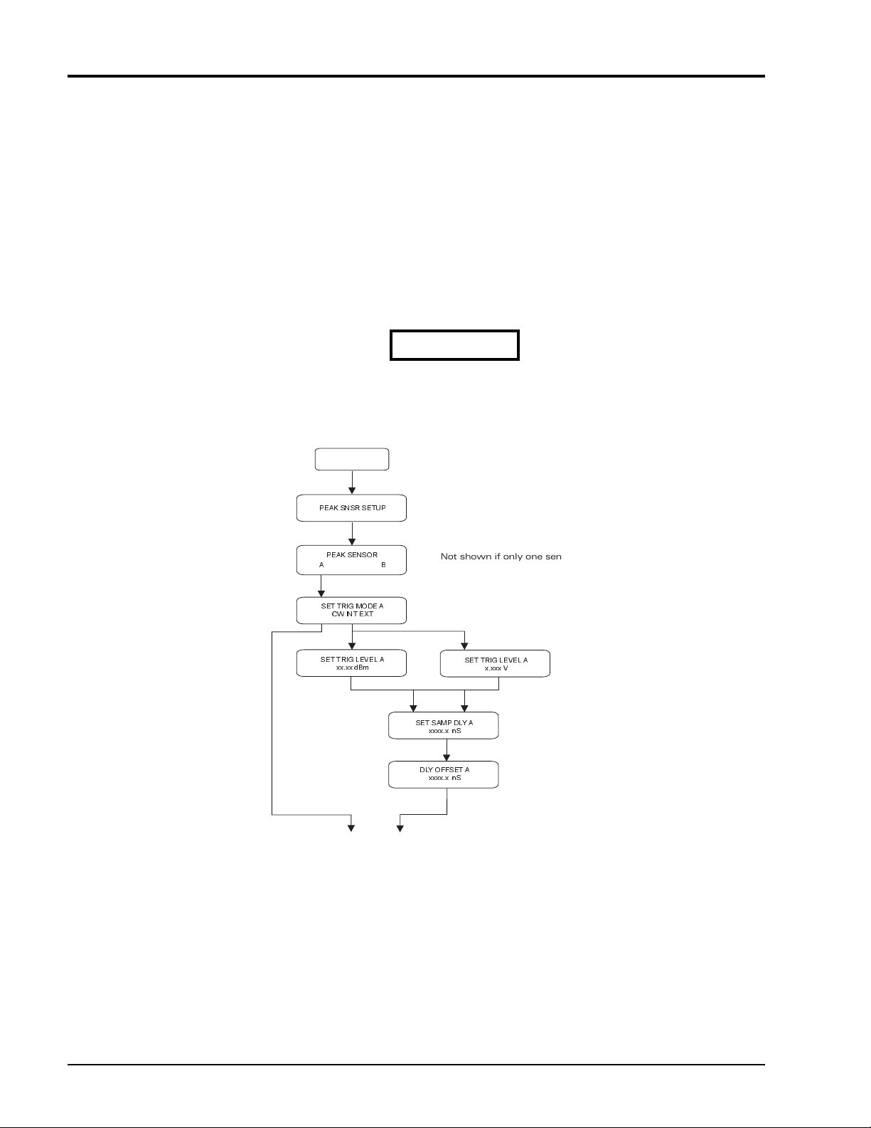
SET UP
PEAK SNSR SETUP
PEAK SENSOR
A
SET TRIG MODE A
CW INT EXT
SET TRIG LEVEL A
xx.xx dBm
To default display
B
Not shown if only one sensor is attached
or if the power meter is single- channel (8541)
SET TRIG LEVEL A
x.xxx V
SET SAMP DLY A
xxxx.x nS
DLY OFFSET A
xxxx.x nS
Figure 2-1: Sensor Setup Menu Tree
2-2 Manual 21568, Rev. F, March 2008
Page 27

2.2.2 Triggering
The 8540 power meters will not display a new peak power reading until the 8035XA sensor is
triggered. The default configuration is internal triggering (INT) at -20 dBm. Press [MENU],
select SETUP MENU, select PEAK SNSR SETUP, (select sensor A or B if necessary), and then
select INT triggering. You can then enter a new internal trigger level. Be sure that the value is 3
dB or greater below the peak powe r level of the signal being measured. If you are attemptin g to
trigger at excessively low power levels, measurement repeatability and noise performance can
be improved by using external (EXT) triggering.
INT Trigger Level
Operation
Amplitude Profile of
Meaured Signal.
Figure 2-2: Internal Triggering Levels
Manual 21568, Rev. F, March 2008
Page 28

Series 8035XA Peak Power Sensors
This is a pproximately 0.0 ns delay.
A built in delay line provides at least
20 ns look-ahead capability.
Sample Delay Pulse
10 sµ
Delay
58542 VXIbus Power Meter SCPI Compatible Commands
OUTPUT @Pwr_MTR;SENS1:TRIG:SOUR INT
OUTPUT @Pwr_mtr, SENS1: TRIG: DEL 10E-06
WAIT 200
OUTPUT @Pwr_mtr, MEAS1?
ENTER @Pwr_mtr: Peak_pwr_rdg
! Selects Internal Triggering
! Sets Sample Delay Position to 10 s
! Wait 200 ms for Sample Time Set
! Take a Measurement
µ
RF
Envelope
Trigger Level
(Int. or Ext.)
2.2.3 Zeroing
Zero the sensor before taking critical measurements in the bottom 10 dB of the peak power
sensor’s dynamic range. For standard peak power sensors, this level is -10 dBm.
When making dual channel power measurements, zero the sensors whenever another sensor
is attached or disconnected. Use the following steps:
1. Turn off the RF source.
2. Press [CAL/ZERO].
The sensors will zero automatically. The 8540 power meters detect when a sensor is attached
to the calibrator port. When a sensor is not attached to the power sweep calibrato r, the power
meter automatically initiates the zeroing procedure (if only one sensor is connected to the
meter). Be sure to deactivate the RF source for zeroing. Leaving the sensor attached to your
measurement test ports during zeroing properly accounts for test setup ground noise an d metal
to metal contact thermal EMF.
The 8035XA Series EXT trigger port is on the back of the sensor , not the power meter. A set of
three SMB(f) to BNC(m) cables are included with each 80 35XA Series senso r. The EXT tr igger
input impedance is 110 kΩ. This allows you to use TTL level signals without damaging the inp ut
circuit. However, the input impedance match might cause triggering line reflections and
potential false triggering when fast (50 Ω) trigger sources are used.
This can be resolved by setting the EXT trigger level (see Figure 2- 1).
The CW power measurement mode is also selected in the Peak Sensor Setup menu. CW
measurements are automatica lly performed on a continuous basis.
2-4 Manual 21568, Rev. F, March 2008
Figure 2-3: 8035XA Sensor Timing Diagram
Page 29

2.2.4 Sensor Triggering
A measurement will not be possible until the peak power sensor is triggered. The Series 8540
Power Meters will display
verification technique is valid for both Series 8540 and 58542 VXI Power Meters:
1. If you need to verify triggering, connect the Sample Delay output on the back of the
8035XA Series sensor to an oscilloscope using one of the SMB(plug) to BNC(m)
cables provided with the sensor. Set the scope channel to dc coupling, 1.0 µs per
division. Use rising edge (Normal) triggering at about 0.5 V trig ger level. Set the sens or
sample delay to 2.0 µs.
2. The sample delay pulse will appear each time the sensor is triggered. If a pulse does
not appear on the scope display, the sensor is not triggering. Check the triggering
configuration and adjust it if necessary. An analog oscilloscope may show a dim trace
when the repetition rate is low.
3. A quick check that can be made on the 8540 power meter for triggering without using
an oscilloscope is to press [dB/mW] twice. This will clear the current reading and
display
NO TRIG until a valid trigger is received.
Operation
NO TRIG until a valid trigger is received. The following trigger
Manual 21568, Rev. F, March 2008
Page 30
Series 8035XA Peak Power Sensors
2.3 Sample Delay
Sample Delay is the time value in nano-, micro-, or milliseconds that appears on the Series
8540 display after an 8035XA Series sensor has been calibrated. This is the length of time
between the trigger point and the sample point on the pulsed signal. This capability allows you
to measure the power level of your pulsed sig nal at any time point along its amplitude path. The
power level displayed is the true, sampled signal level at the time position that you specified;
the pulse level is not interpolated from two adjacent samples as is com mon in random sampling
oscilloscope-type peak power meters.
Sample delay is fully adjustable from -20 ns to 100 ms. On the 8541/2 front panel, use the
arrow keys to position the cursor and adjust the time values. Seven digits, four to the left of the
decimal and three to the right of the decimal, can be edited in the microsecond (ns) and
millisecond (ms) ranges (see Figure
allows four digits to the left of the decimal, but only a .0 or .5 to the right of the decimal.
The 0.0 ns time delay setting will be close to the trigger level when internal triggering is used. If
your measurements require definition of the 0.0 ns position, use Sample Delay Offset to adjust
for small triggering variations.
2-4 for an example.) The nanosecond range
Figure 2-4: Sample Delay Adjustment Display
Full 0.5 ns resolution is always possible regardless of the front panel units disp lay. On the
millisecond ranges, small nanosecond level increments in sample delay can be performed by
incrementing Sample Dly Offset in the Peak Sensor Setup menu tree. In addition to allowing
control of small nanosecond range sample delay increments while currently displaying
millisecond ranges, sample delay offsets allow you to compensate for cabling and circuit time
delays in your test setup. The sensor delay is the sum of DLY
and DLY OFFSET
)
B
and DLY OFFSETA (or DLYB
A
2-6 Manual 21568, Rev. F, March 2008
Page 31

2.3.1 Sample Delay Display
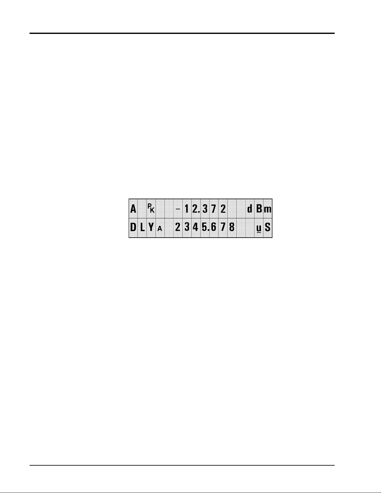
With a single peak power sensor attached, the default display after attachment and calibr ation
of the sensor will have the power displayed on one line and the sample delay displayed on the
other line. The default for channel A will be as shown in Figure
The default for channel B will be as shown in Figure 2-6.
Operation
2-5.
Figure 2-5: Channel A Default Sample Delay
Figure 2-6: Channel B Default Sample Delay
The default displays will also be used when the meter is preset. The default for two sensors will
display power readings on both lines as shown in Figure
Figure 2-7: Channel A & B Default Sample Delay
2-7.
If a sensor is uncalibrated, the word UNCALIBRATED will be displayed for the channel as
shown in Figure
2-8.
Figure 2-8: Sample Delay with Uncalibrated Sensor
Manual 21568, Rev. F, March 2008
Page 32

Series 8035XA Peak Power Sensors
The default display will be presented after attachment of a new sensor. Sample delay offsets
are available for each sensor. The use of a non-zero offset will be indicated by an asterisk
between the last digit and the units as shown below. The delay displayed is the sample delay
before the application of any offset.
DLYA 56.345*uS
The Sample Delay display line interacts with the Min/Max display line. If Min/Max is turned on
for a line that Sample Delay was tracking, Min/Max will be displayed instead of Sample Delay.
2.3.2 Setting Sample Delay
The sample delay can be set from two locations within the menu structure. One location is at
the default display where sample delay information is displayed. The other is in the menu
structure where the peak sensor setup is configured.
Sample Delay Operation
You will be presented with a display with a decimal point fixed in the display. Normally, four
digits are available to the left of the decimal point and three digits to the right as shown below.
Leading zeros will be suppressed.
XXXX.XXX uS
When the units are set to nS, only one digit will be available to the right of the decimal.
The right and left arrow keys move a cursor to select a digit or unit to be changed. The cursor
will stop only at valid digit or unit locations (valid digits are shown by ^ below). The cursor will
stop under valid blank spaces so that large numbers can be entered quickly.
XXXX.XXX uS
^^^^ ^^^ ^
Press the up key to increment the digit value b y 1, or the down key to decrement the digit value
by 1. If a digit is incremented past 9, a carry is propagated to the next higher digit (odometer
mode). Similarly, if a digit is decremented past 0, a borrow will be made from the next higher
digit. You can decrement the delay to a negative number.
An exception is made when the cursor is moved to the 10 ths of n anose co nd s ran ge. The up or
down arrows will change the display in .5 nS increments. This is the maximum resolution of the
sensor.
Press the up or down keys while the cursor is und er the units display to cycle through th e units.
You will be offered a choice of nS, uS, or mS. The units display does not wrap around.
The units selected will be used in all displays for the delay for the sensor to which they are
assigned.
If a peak measurement parameter is changed, e.g. sample delay or trigger level, the power
display will display NO TRIG (see Figure
parameters in effect. If the sensor triggers quickly, the message may not be seen. In the TR2
2-8 Manual 21568, Rev. F, March 2008
2-9) until a new measurement is made with the new
Page 33

mode, the display may show MEAS* with the asterisk lines rotating as each measurement is
made.
The GPIB will return numerical data in the No Trig state, depending on the GPIB measurement
mode. See the GPIB Commands in Section
2.3.3 Sample Delay Limits
There is no automatic units scaling for the sample display. You can enter an y number up to
9999.999 and then set the units, with the exception of the nS range , which allows only one digit
to the right of the decimal. If the sample delay plus the offset exceed the range of the attached
sensor, the
Figure
is too low.
S at the end of the line will be replaced with an arrow indicating a range error (see
2-10). An up arrow indicates that a delay is too high, a down arrow indicates that a delay
Operation
Figure 2-9: Sample Delay with No Trigger Display
2.4 for more details on Trigger Modes.
Figure 2-10: Sample Dely Over-Range Indication
When the arrow keys are used to change the units, the digits in the display will simply use the
new units. The only exception is going from µS to nS. The digits to the right of the decimal point
will be reduced to one digit, and that last digit will be either 0 or 5 as shown in the following
example:
Starting Display Action Resulting Display
15.678 uS ↓ 15.5 nS
Setting Delay from the Default Display
A cursor will be displayed on the sample delay in the default display. When you change the
sample delay by pressing an up or down arrow key, the associated sensor will be immediately
programmed with the new delay. The power display may be repla ced with NO TRIG until a new
power measurement can be made with the new sample delay.
If an over-range sample delay is entered, no measurement will be made until the over-range
condition is corrected (over-range includes delay plus offset).
If there is more than one delay display line, the left and right arrows will move the cursor off the
end of one display line and onto the next.
Manual 21568, Rev. F, March 2008
Page 34

Series 8035XA Peak Power Sensors
Setting Delay from the Peak Setup Menu
The cursor will be available immediately upon entering this menu. The sensor will not be
updated with the new delay setting until the peak menu sequence is completed. This requires
selecting the trigger mode, setting the trigger level, setting the sample delay, and setting the
sample delay offset. The display will exit to the default measurement display when you press
[ENTER] on the last menu in the sequence.
2.3.4 Setting Sample Delay Offset
The sample delay offset is settable from the menu following the SET SAMP DLY menu (see the
Menu Tree in Figure
to enter the sample delay. You can change a set of digits (XXXX.XXX), plus units.
The offset will be range checked together with the sample delay so that the total of sample
delay plus offset does not exceed the range of the sensor. If the range of the sensor is
exceeded, a beep may sound and an arrow will replace the S at the end of the line (see Figure
2-11) to indicate an out of range condition. If you exit the menu without correcting the out of
range condition, no power measurement will be made.
2-1). The method to enter the delay offset will be the same as the method
Figure 2-11: Sample Delay Over-Range Offset Display
For example, if the max delay available from a sensor is 100 mS and the samp le delay is set to
75 mS, the maximum offset permitted is 25 mS. Anything larger will cause an arrow to be
displayed.
Each sensor has its own delay offset paramet er.
2.3.5 Single Peak Sample Measurements
Measurements for a peak sensor will be performed over a number of single samples. A single
sample is defined as follows:
1. The sensor is armed.
2. A pulse is triggered and sampled by the sensor. The sensor informs the meter via handshaking
that a measurement voltage is available.
3. The meter measures the voltage and computes the power from this one trigger sample.
When averaging is turned on, the averaging will be done over a number of single samples. Auto
averaging will use an increasing averaging number as the power level being measured
declines. For example, the number of sam ples req u ire d fo r me as ur em e nt s at 20 dBm is 1. At 20 dBm, the number of samples will be about 32 (this could change depending on mode or
software version).
2-10 Manual 21568, Rev. F, March 2008
Page 35

2.3.6 Real Time Pulse Profile and Sample Position Display
The Detector Out connector on the rear of the 8035XA Series Peak Power Sensor can be
connected to any common oscilloscope for a real-time amplitude profile of your signal, delayed
by about 120
Connect the SMB to BNC cables to your oscilloscope (digital scope preferred - especially for
sample delay setting >500 µs) as shown in Figure
ns.
2-12.
Operation
Figure 2-12: Pulse Profile and Sample Delay Test Setup
Use the Sample Delay output as an oscilloscope trigger source. This waveform rises at the
trigger point and falls at the sample point; thus, it provides both a stable scope trigger source
and a precise indicator of the trigger point and sample point.
The time length of the sample delay pulse is the sum of the sample delay which is displayed on
the Series 8540 power meter front panel, and the sample delay offset which is available
through the menu.
Manual 21568, Rev. F, March 2008
Page 36

Series 8035XA Peak Power Sensors
2.3.7 Sample Delay Offset
In addition to compensating for delay line triggering variations or external triggering cables,
sample delay offset can be used to set a 0.0 ns time refe rence p oint a fter the tr igger poi nt (see
Figure
2-13).
t
total
t
total = sample delay + sample delay offset
t
total = 20,000 s + 0.120 s = 200 120 sµµ µ
or
t
total = 200,000 s + (-0.010 s) = 199.990 sµµ µ
Figure 2-13: Sample Delay
The use of a digital oscilloscope can permit better viewing of data. There are two small markers
injected onto this waveform. The first is a small triggering marker which is added slightly after
the trigger point. The second marker on the waveform is the sample marker. The sample
marker is located slightly behind the actual sample point. There may be small markers at the
end of the sample transfer and when the trigger signal occurs. Because the visibility of these
markers varies greatly with signal level and horizontal sweep rate, the use of the SAMPLE
DELAY output is recommended.
In Figure 2-14, triggering occurs at the frame start of a pulsed TDMA communications signal.
The trigger level is set such that triggering can only occur on the highest amplitude pulse; this
provides stable triggering. A sample delay offset is used to set a 0.0 ns reference point at the
start of the third data burst pulse.
Sample
Delay
Sample
Delay
Detector Out
Connection
Internal
Trigger
Level
Sample Delay Offset
Sample Delay
Connection
Figure 2-14: Using SD to Offset a 0 ns Time Refer ence
2-12 Manual 21568, Rev. F, March 2008
Page 37

2.3.8 Measuring Pulse Droop
Detector Out
Trigger Level
t
1
t
2
Pulse characteristics such as droop, ripple, and overshoot can be measured quickly using
referenced measurements. This involves the use of the fron t panel REL key for the Series 85 40
power meter users, or the CALC#:REF:COLL function for 58542 power meters.
1. Connect the 8035XA Peak Power Sensor to the power meter and the CALIBRATOR
output.
2. Press [CAL/ZERO] to calibrate the sensor to the meter.
3. Upon successful completion of power sweep calibration, connect the sensor to a pulsed signal
source. The power level must be above the trigger level.
4. Connect the 8035XA Detector Out and Sample Delay leads to a digital oscilloscope.
5. Set the sample delay ( DLYA) to the t1 position just after the rising edge as shown in Figure
2-15.
6. Press [REL]. The display should now read approximately 0.00 dBm or 100%.
7. Set the sample delay to the t2 position just before the falling edge of the pulse.
Operation
The display is now reading the pulse-top amplitude variation.
Figure 2-15: SD Setting for Measuring Pulse Droop
Manual 21568, Rev. F, March 2008
Page 38

Series 8035XA Peak Power Sensors
100% Reference Level
3 dB down (50%)
3 dB down (50%)
Sample Delay
Offset
Total Delay
Trigger Level
Sample Delay = Pulse Width
t
t
=
2.3.9 Measuring 3 dB Pulse Width
Pulse width and other pulse timing parameters can be measured using the REL key and the
sample delay offset control (see Figure
1. Preset the delay offset to 0 nS.
2. Set the sample delay equal to about half the pulse width.
3. Press [REL] to set the 0.0 dB reference level (100% for Watts display).
4. Set the sample delay to a position on the rising edge of the pulse. Increment or decrement the
sample delay value until the power level display reads approximately -3.00 dBr.
5. Remember or write down the sample delay value.
6. Press [MENU], and use the up/down arrow keys to display SETUP MENU. Press [ENTER].
Select PEAK SNSR SETUP, then select the current tri ggering m e tho d (INT or EX T). When
DLY Offset appears, set the offset value to the same time value from Step 4. This sets the 3 dB
down time point to a 0.0 ns reference position.
7. Press [ENTER] to return to the measurement display.
2-16).
8. Set the sample delay to a position on the falling edge of the pulse. Increment or decrement the
sample delay value until the display again reads approximately -3.00 dBr.
The sample delay currently displayed is the signal’s 3 dB pulse width.
Figure 2-16: Using SD to Measure a 3 dB Pulse Width
2-14 Manual 21568, Rev. F, March 2008
Page 39

2.3.10 Measuring Rise-Time
Rise time measurements can be performed using a technique similar to the pulse width
measurement. This example uses a linear Watts display readout rather than the more common
logarithmic dBm readout for convenient identification of the 10% and 90% levels.
1. Preset the delay offset to 0 ns.
2. Press [dBm/mW] to obtain a linear, Watt, display readout.
3. Set the sample delay equal to about half the pulse width.
4. Press [REL] to set the 100% reference level.
5. Set the sample delay to a position on the rising edge of the pulse. Increment or decrement the
sample delay value until the power level display reads approximately 10%.
6. Remember or write down the sample delay value.
7. Press [MENU]. Select SETUP MENU then PEAK SNSR SETUP. Proceed to the SAMPLE
DELAY OFFSET selection. Set the offset value to the same value from Step 6.
Operation
8. Return to the measurement display and increment the sample delay until the display reads
approximately 90%.
The sample delay currently displayed is the 10% to 90% rise time.
2.4 GPIB Commands
These commands supplement the commands given in the Series 8540C Universal Power
Meter Operation and Maintenance Manual.
2.4.1 Setting Trigger Modes
These commands set the trigger method for the 8035XA sensor. The sensor can be set to
trigger on the rising RF envelope of the power signal. This is the internal trigger mode. An
external TTL trigger can be used, or the sensor can “free run” and allow a CW measurement
mode with no trigger required.
The terms digital filter (as used in some instrument instructions) and averaging buffer (as used
here) are interchangeable.
Examples:
OUTPUT 713;PEAK A INT TRIG -10.00 ! Configure sensor A for internal trigger at
! -10.00 dBm trigger level
OUTPUT 713;PEAK B EXT TRIG 1.50 ! Configure sensor B for external trigger at
OUTPUT 713;PEAK A CW ! Configure sensor A for CW measurements
In this example, the address 713 means "Type 7" GPIB instrument, and address 13 for the
power meter. The GPIB control command (the portion to the left of the semicolon) may vary.
Trigger Modes With a Peak Sensor
Manual 21568, Rev. F, March 2008
! 1.50 Vdc trigger leve l
Page 40

Series 8035XA Peak Power Sensors
Examples:
OUTPUT 713;TR3 ! Last measured value will be returned
OUTPUT 713;TR2 ! Refill averaging buffer before measurement display
OUTPUT 713;TR1 ! Wait for trigger before returning measurement
OUTPUT 713;TR0 ! Measure, but no display
TR0
The meter will measure power, but the display of measured data will be suppressed and the
GPIB bus will not be updated with measurement data.
TR1
This mode will wait until the sensor triggers before returning a measurement. The
measurement returned will be after the application of any averaging. The display for the
channel will follow the TR1 mode. When TR1 is received over the bus, NO TRIG will be
displayed until the sensor has triggered and measurement data is available.
TR2
This mode will wait until enough measurements are made to completely refill the averaging
buffer. The measurement returned will be the average of all measurements in the buffer.
MEAS* will display with one of the asterisk lines rotating for each measurement) while the
averaging buffer is being filled.
TR3
The last measured value will be returned. This mode will not wait for the peak sensor to trigger.
2.4.2 Setting Delays
When the sensor is configured for internal triggering, the delay from trigger to measu rement
sample must be set. The valid range of delays is -20 ns to 100 ms, expressed in a floating point
number. The smallest delay increment is 0.5 ns. Setting delays in CW trigger mode are invalid
and ignored.
Examples:
OUTPUT 713;PEAK A DELAY 1.20E-6 ! Configure sensor A for a delay of 1.20 µs
OUTPUT 713;PEAK B DELAY 33.5E-9 ! Configure sensor B for a delay of 33.5 ns
The offset command adds a known offset to the trigger delay value. The actual value of delay
would be the DELAY set plus the OFFSET set. The default value of offset is 0. The valid range
of offset is -20 ns to 100 ms, expressed in a floating point number.
Example:
OUTPUT 713;PEAK A OFFSET 1.00E-6 ! Configure sensor A for a delay offset of 1.00 µs
2-16 Manual 21568, Rev. F, March 2008
Page 41

2.4.3 Reading Values
These commands read the current settings of delay or offset.
Examples:
OUTPUT 713;PEAK A? ! Query the current sensor A trigger setting
ENTER 713;TRIG$ ! Query the trigger mode setting of the sensor, and return:
CW
or
INT_TRIG
or
EXT_TRIG
OUTPUT 713;PEAK A DELAY? ! Query the current sensor A delay setting
ENTER 713;Delay
OUTPUT 713;PEAK B OFFSET? ! Query the current sensor B offset
ENTER 713;Offset
Operation
Manual 21568, Rev. F, March 2008
Page 42

Series 8035XA Peak Power Sensors
2.4.4 Commands for the 58542
The following peak power sensor GPIB commands are used with the Model 58542 VXI
Universal Power Meter. Refer also to the Model 58542 Operation and Maintenance Man ual for
additional details.
SENSe<sensor 1 or 2>:TRIGger:SOURce<INTernal|EXTernal|CW>
This command sets the sensor (1 or 2) peak trigger mode to either the INTernal, EXTernal, or
CW mode.
SENSe<sensor 1 or 2>:TRIGger:DELay[:MAGnitude]<1e-6, -20e-9,100e-3>
This command sets the sensor (1 or 2) peak delay value to any desired time from -20e-9 to
100e-3 seconds, with 1e-6 seconds being the default setting.
SENSe<sensor 1 or 2>TRIGger:OFFSet[:MAGnitude]<0, -20e-9,100e-3>
This command sets the sensor (1 or 2) trigger offset time to any desired value from -20e-9 to
100e-3 seconds, with 0 seconds being the default setting.
SENSe<sensor 1 or 2>TRIGger:LEVel[:MAGnitude]<-10 dBm, -30 dBm, 20 dBm>
When the INTernal trigger mode is in use, this command sets the trigger level to any desired
power level setting from -30 to +20 dBm. Default is -20 dBm.
SENSe<sensor 1 or 2>TRIGger:LEVel[:MAGnitude]<1.700, -0.100, 5.000>
When the EXTernal trigger mode is in use, this command sets the trigger level to any desired
voltage level from -0.100 to 5.000 V. Default is 1.700 V.
2-18 Manual 21568, Rev. F, March 2008
Page 43

3.1 Introduction
This chapter describes the electrical operation of the Series 803 5XA Peak Power Sensors.
Refer to the block diagram in Figure 3-1 to follow the general function of the sensor. The RF
signal is rectified in the sensor element, and the video envelope is buffered and de layed by the
input amplifier and delay buffers. This buffered envelope is available at the Detector Out
connector. The Track and Hold (T&H) function tracks and follows the signal and then holds it for
hundreds of microseconds. The Sample and Hold (S&H) function acqu ires the S&H o utput and
holds it for hundreds of milliseconds.
The timing circuitry generates the sample pulses from the trigger input or, if the sensor is in the
free run mode, from an internal oscillator.
The block diagrams, circuit descriptions, and the troubleshooting information in Chapter 4 are
written around the circuit test points. The delay lines shown in Figure
Analog Timing Diagram in Figure 3-3. Delay lines match the delay through the analog channel
to the sample point, and the delay through the timing circuitry to the sample generator. Since
fixed lumped constant delay lines are used, the match is not perfect. The delay through the
3
Theory of Operation
3-1 are illustrated in the
Manual 21568, Rev. F, March 2008
Page 44

Series 8035XA Peak Power Sensors
INTernal trigger is slightly longer than the delay through the EXTernal trigger due to the delay of
the input differential preamp.
Figure 3-1: 8035XA High Level Block Diagram
3.2 Analog Assembly Description
Refer to Figure 3-2, the Analog Timing Diagram in Figure 3-3, and schematic diagram #21351
in Chapter 7 to follow the discussion of the Analog PC assembly circuit operation.
The rectified signal from the detector goes into the resistors R1 or R2 (TP1 and TP2). The
signal sees 2 kΩ to ground from either input (the negative input sees 2 kΩ to a virtual ground
inside R100). R3 helps to balance the input bias current. U1 and U2 delay the signal so the
trigger output and video output may be viewed close together. U4 and U5 are buffers for the
delay lines (TP3).
3-2 Manual 21568, Rev. F, March 2008
Page 45

Theory of Operation
U10C and U7A provide a fast Track and Hold (T&H). U7A buffers the T&H capacitor C21, and
U7B buffers the S&H capacitors, C1 & C2.
Figure 3-2: Analog PC Assembly Block Diagram
A track and hold differs from a sample and hold in the manne r in w hic h the sign al pr ior to the
hold is manipulated. In a sample and hold, the sample gate turns on and the holding capacitor
is charged to the signal potential, then the sample gate turns off and the hold capacitor
maintains the value of the input at the time of the sample. In a track and hold circuit, the voltage
on the hold capacitor is the same as the input (tracks) until the track gate goes off, after which
the level is held until the track goes on and the hold capacitor again follows the input.
The INTernal or EXTernal trigger source is selected by U10D and U11A. U11B functions as a n
inverter for HIGHGAIN. U6 amplifies the trigger signal by 1 or 41. Trigger DAC U9 is loaded
with a count from the serial chain. The DAC needs the data signal held after the clock for at
least 80 ns. A2R12 and A2C25 on the Digital board take care of that requirement. That cou nt
gets translated into a voltage between - 0.1 V and about +5 V by U8A. Digital bo ard comparator
A2U18 provides the TRIG-IN pulse (A2TP25). A2R42 provides hysteresis for A2U18.
*
NOTE: All times shown in Figure 3-3 are referenced to TP3, and are not to scale.
Manual 21568, Rev. F, March 2008
Page 46

Series 8035XA Peak Power Sensors
NEG INPUT
TP1
POS INPUT
TP2
DIF - AMP
TP3
1ST DELAY
TP4
2ND DELAY
TP5
MONITOR
TP9
TRACK&HOLD
TP7
OUTPUT
TP12
TRIG AMP
TP6
SAMP
J2-5
DELAY TIME
TRANSFER TIME
Figure 3-3: Analog Circuit Timing Diagram
3-4 Manual 21568, Rev. F, March 2008
Page 47

3.3 Digital Assembly Description
3.3.1 Overview
Refer to the Digital PC block diagram in Figure 3-4, an d the Digital Timing Diagra ms in Figur es
3-5, 3-6 and 3-7.
The digital board provides the timing functions for delays between a small negative time (with
respect to either the video monitor, or the sampled pulse) and >100 ms. In the CW mode, the
digital board is not reset, but continues to generate clocks and samples at about 70 µs
intervals. In either the INTernal or EXTernal modes, an acquisition is requested by the host (the
power meter to which the sensor is connected is the host) which causes READY to be set.
When an input trigger is received, it is latched and delayed by a FINE delay, and then starts a
10-MHz clock. The clock increments a COARSE counter until it reaches FFFFF or all ones, and
then outputs a Ripple Carry Out (RCO) signal. This is latched as SAMPle, delayed by one
count, and then compared to the count of 51µs out of the counter to allow the SAMPle to be
51µs wide. Then the COARSE counter is reLOADed for about 5µs, the 10-MHz clock is
stopped for about 5µs, the
reset for about 1µs. A 48-bit serial stream provides the 80350A configuration infor mation. When
the serial clock is running, CLKHOLD resets the TRIG loop and loads the counter.
LOAD unasserted, and the TRIGger, SAMPle, and READY flip-flops
Theory of Operation
*
NOTE: Over-score indicates a logic-NOT condition.
Manual 21568, Rev. F, March 2008
Figure 3-4: Digital PC Assembly Block Diagram
Page 48

Series 8035XA Peak Power Sensors
3.3.2 Description
When READY (TP17) is true, U8B flip-flop (TP14 - TRIG) is set after TRIG-IN goes high. U13
delays the TRIGgered signal by a delay programmed in 1/2 ns intervals. U3 is a 10-MHz gated
delay line oscillator which, when enabled by the fine delay, clocks (TP1) the coarse counter U1,
U5, U6, U15 and U16, and the SAMPLE flip-flops U7B and U8A. Unlike conventional oscillators
which free run, a gated delay line oscillator beginning time period is the same length as all of its
other time periods with the possible exception of the last period when enable is unasserted.
When RCO (TP8) is true for one clock cycle (ignores pulses less than 100 ns), U7B is latched
as SAMPle (TP11). SAMPle is delayed by one count because 51µs (TP7) can still be true when
SAMPle goes true, and AND’d with 51µs from U1. When true (when SAMPle has been on for
51µs), the U10A loader receives a negative edge clock.
asserted and held low via U9C, R34, and C27 until the 10-MHz clock (U3) stops via U12A,
U10B, (TP9), U4A, and U4C. Note the sequence:
1. CTR-CLK (TP1) must be running.
2. LOAD-CTR (TP9) goes low and stays low while CTR-CLK continues for at least one cycle.
This loads the COARSE counter.
3. CTR-CLK (TP1) stops. LOAD-CTR is still low. CTR-CLK continues in the CW mode.
LOAD for the COARSE counter is
4. LOAD-CTR returns high at least 200 ns before POST (TP5) returns high. The same FINE delay
which delayed the start of the 10-MHz clock now works against turning the 10-MHz clock off.
SAMP (TP11) going high turns the Track and Hold (T&H) to Hold on the Analog board, and
turns the Sample and Hold (S&H) to Sample. When it goes low, the T&H goes back to tracking
the input and the S&H holds the sampled signal level. U10B POST (TP5), the major reset
circuit, resets READY (TP17) to prevent the trigger circuit from restarting, continues to rese t
TRIG (TP14) (except in the CW mode) which started in PRE-POST, and resets SAMP (TP11).
When the host has read the data, the DATA-IN line is momentarily pulsed low by the host which
sets READY (TP17), and pulls the DATA-IN line (TP20) low via diode CR3. Note that the
DATA-IN — READY handshake does not occur in the CW mode.
EEPROM U11 stores the sensor type, serial number, and calibration constants. This IC is only
accessed by the host. Except for device start and stop conditions, DATA-IN can change states
only when CLK is low. After device stop has been sent, the host sends a 48-bit serial str eam to
set up the 80350A sensor. Four zeros are sent followed by the 12 DAC tr igger bits, followed by
the fine counter 8 bits, 20 bits for the COARSE counter (with FFFFF meaning zero delay), and
finally the 4 control bits (INTernal, EXTernal, CW, and HIGHGAIN). Because the serial DAC on
the ANALOG board has a data hold requirement of 80 ns minimum, DATA-4 (TP2) must be
delayed by R12 and C25.
Incoming CLK turns on U3 (10 MHz - TP1) and U9C (LOAD) (TP9) via U12B (CLKHOLD)
which loads the COARSE counter with the new delay.
The test points are essentially in order across the len gth of bo th the Analog and Digital boar ds
in the approximate order of signal progression to aid in troubleshooting. In addition, the
between-the-board connectors can be used as test points.
3-6 Manual 21568, Rev. F, March 2008
Page 49

Theory of Operation
Figure 3-5: Digital Timing Diagram, INT/EXT Trig Mode
Manual 21568, Rev. F, March 2008
Page 50

Series 8035XA Peak Power Sensors
Figure 3-6: Digital Timing Diagram, CW Mode
Figure 3-7: Digital Serial Data Cycle Timing Diagram
3-8 Manual 21568, Rev. F, March 2008
Page 51

4.1 Introduction
Information in this section is useful for periodic evaluation of the performance and/or r eceiving
inspection testing of the 8035XA Series Peak Power Sensors. These tests assume that the
operation of the particular 8540, 8650, Series Power Meter or Model 58542 VXI Power Meter
being used with the sensor has already been verified as described in the power meter’s
Operation & Maintenance Manual. Verifying the Frequency Cal factors stored in the sensor
EEPROM is not covered in this procedure. If necessary, the Cal Factors should be verified with
a Vector Network Analyzer using similar procedures as for standard power meter sensors.
Before starting these tests, connect the Peak Power Sensor(s) to the compatible power meter,
and allow at least 24 hours for warm-up. These tests will only be valid if the power meter and
the sensor(s) have been calibrated at an ambient temperature between +20 °C and +30 °C
(+68 °F to +86 °F), and are operating within ±3 °C (±5.4 °F) of the calibration temperature.
4.2 Equipment Required
4
Calibration and Testing
The following items of test equipment (or equivalent) are required for completing the
Performance Tests described in this chapter.
Description Instrument Model Requirements
Power Meter Giga-tronics 8650, 8540 or
58542 Series
RF Source Wavetek Model 2510 (Hi
Power Opt.) or equivalent
Oscilloscope (DSO) LeCroy 9400 Bandwidth 125 MHz
CW Thermistor Power
Meter
Thermistor Mount Agilent/HP 478A-H75 0 to +10 dBm range <1.1 SWR
Pulse Generator Wavetek Model 278 or
Attenuators 10, 20, 30 and
40 dBm
Directional Coupler Narda Model 3002, 10 dB
Low Pass Filter Integrated Microwave Model
Agilent/HP Model 432B Inst. Acc. of at least 0.5%
equivalent
Weinschel Model AC118A-
90-33
904 881
Compatible with 8035XA Sensor
+20 dBm @ 50 MHz
Delay and pulse width control
Type N, 0.5 dB accuracy
VSWR <1.20 @ 50 MHz
>50 dB Atten. @ 100 MHz
Manual 21568, Rev. F, March 2008
Page 52

Series 8035XA Peak Power Sensors
4.3 Power Linearity Test
The linearity will be tested in a series of 10 dB steps over the range of the sensor. At low power
levels, the measurements will reflect the uncertainty due the noise and zeroing specifications.
Make a copy of the Performance Verification Data Sheets at the end of this chapter to record
the data from this test.
4.3.1 CW Linearity Test
1. Connect the test setup as shown in Figure 4-8. Set the RF source to 50 MHz. Be sure the sensor
has had at least 24 hours of warm-up time. To take accurate measurements, it is essential to take
out any drift that might occur.
a. Calibrate the Peak Power Sensor as described in the applicable Power Meter Operation and
Maintenance manual.
b. Place the peak sensor into the CW mode.
c. Set the power meter to display power in lin ear units (mW).
d. Set Averaging to 4.
e. Set the CW frequency to 50 MHz.
2. Start with no attenuation between the coupler and the Peak Power Sensor. Record results on the
first row of the linearity data recording sheet. If the sensor being tested is an 80351A, 80352A
or 80355A model, remove the attenuator from the sensor.
3. Turn the RF source off and zero the Peak Power Sensor by pressing [ZERO/CAL].
Figure 4-8: Power Linearity Test Setup
4. Zero the thermistor power meter.
5. Turn the RF source on.
4-2 Manual 21568, Rev. F, March 2008
Page 53

Calibration and Testing
6. Adjust the RF source until the thermistor power meter reads 10.0 mW ±0.25 mW.
7. Record the thermistor power meter reading, P1, and the power meter reading, R1, on the data
sheet.
8. Adjust the RF source until the thermistor power meter reads 1.0 mW ±0.025 mW.
9. Record the power meter reading, P2, and the power meter reading, R2, on the data sheet.
10. Calculate and record the reference power ratio P1/P2, and the DUT reading ratio, R1/R2.
11. Calculate and record the Linearity Error using the formula:
12. Add an additional -10 dB of attenuation between the coupler and the Peak Power Sensor and
repeat Steps 3 through 9, filling in the 10 dB through 40 dB (through 30 dB in Peak Mode)
attenuation rows of the data sheet. On these rows, add the current linearity error to the
accumulated linearity error in the row above. Verify that this accumulated error is less than the
specified values given on the data sheet.
4.3.2 Peak Linearity Test
Set the sensor to EXT, 1.7 V, 10 µs, 0 offset, and connect the TRIGGER IN (black lead) to the
pulse generator. Set the pulse generator to 1 kHz, and repeat all of the steps in the CW
Linearity Test for this Peak Linearity verification test. Record the readings on the Peak Linearity
Data recording sheet at the end of this chapter.
Manual 21568, Rev. F, March 2008
Page 54

Series 8035XA Peak Power Sensors
4.4 Trigger Modes Tests
Connect the test setup as shown in Figure 4-9. Set the pulse generator for a 100 Hz pulse
repetition frequnecy. Set the RF source to generate a 2 ms wide pulse. Set the power me ter to
display power in linear units (mW). Set teh source to 50 MHz with a power output to
approximately 1 mW (0 dBm).
1. Set the delay of the pulse generator to 0 ms.
2. Set the peak Power Sensor to EXT trigger mode with the following parameters:
Trigger level: 1 V
Trigger Delay: 1 mS
Delay Offset: 0 mS
NOTE: If the sensor under test is has an external attenuator, remove it before
connecting to the sensor to the RF source.
DC
Figure 4-9: Detector Output and Trigger Level Setup
4.4.1 Detector Output Test
Leave the test setup as shown in Figure 4-9. Connect the 1 MΩ oscilloscope input to the
Detector Output. Verify that the pulse has an amplitude of approximately 200 mV peak to p eak
for an applied signal level of 0 dBm.
4.4.2 Trigger Level Test
The following tests check for trigger sensitivity. Each section refers to a specific sensor group
arranged by power capability. Refer to the appropriate section based on the sensor model
being verified.
4.4.2.1 100 mW Power Peak Sensors
Set the RF source to the following settings:
4-4 Manual 21568, Rev. F, March 2008
Page 55

50 MHz, -30 dBm
Pulse output settings:
PRF 100 Hz
Width: 2 msec
Pulse State: ON
NOTE: Applies to 80350A, 80353A and 80354A sensors only.
1. Set the Pulse Sensor trigger to Internal and sample delay to 1 ms.
2. Set the sensor trigger level to -5 dBm. Set the pulse amplitude of the RF source to 0 dBm
and verify triggering by noting that the sample delay pulse is present
3. Set the RF source level to -20 dBm verify triggering does not occur.
4. Set the sensor trigger level to -10 dBm and set the RF source level to 0 dBm and ve rify
trigger operation.
5. Set the Pulse Sensor to external trigger (EXT TRIG). Set the sensor external trigger level to
1.7 V
DC. Verify triggering with +5 V pulse input. Set the input level to 0 dBm. Verify that the
sensor is triggered and the meter displays a valid power reading.
6. Disable the external trigger then set the input level to -10 dBm. Verify that the sensor is not
triggered. The peak sensor should not trigger.
4.4.2.2 High Power Peak Sensors
Calibration and Testing
Set the RF source to the following settings:
50 MHz, -30 dBm
Pulse output settings:
PRF 100 Hz
Width: 2 msec
Pulse State: ON
NOTE: Applies to 80351A, 80352A or 80355A sensors only.
1. Remove the attentuator before connecting the sensor to the pulse source. Do not
exceed +23 dBm peak input power to the sensor.
2. Set the Pulse Sensor trigger to Internal and sample delay to 1 ms.
3. Select the appropriate table on the datasheet based on the model number of the sensor
being tested.
4. Set the sensor trigger level to +15 dBm for the 80351A sensor and +25 dBm for the
80352A and 80355A sensors. Set the syntehsizer level to 0 dBm and verify trigger
operation.
5. Set the RF source level to -20 dBm and verify triggering does not occur.
6. Set the trigger level to +10 dBm for the 80351A sensor and +20 dBm for the 80352A and
80355A sensors. Set the RF source level to 0 dBm and verify trigger operation..
7. Set the Pulse Sensor to external trigger (EXT TRIG). Set the external trigger to 1.7 VDC.
Verify triggering with +5 V pulse input. Set the input level to 0 dBm. Verify that the sensor
is triggered and the meter displays a valid power reading.
8. Disable the external input trigger then set the RF source level to -10 dBm. Verify that the
sensor is not triggered. The peak sensor should not trigger.
NOTE: Reset the sensor trigger when testing for a non-triggered state after the sensor has
been triggered. Resetting the sensor trigger can be acheived by varying the sample delay by
Manual 21568, Rev. F, March 2008
Page 56

Series 8035XA Peak Power Sensors
0.1 nsec on the 8650A or 58542 power meters or by pressing the Enter button on the 8540C
power meter.
4.4.3 Delay Test
The Upper and Lower Limits in Table 4-8 are the minimum tolerances to test Delay
functionality.
NOTE: The following test is suggested to verify sensor delay functionality. Sensor delay
accuracy is unspecified.
1. Connect sensor to channel A of the power meter, and then calibrate the sensor. If an
80351A, 80352A or 80355A sensor is being tested, remove the attenuator.
2. Select PRESET from the RECALL menu.
3. Connect the sensor to a pulse generator with a 0 dBm, 50 MHz, 2 ms pulse.
4. Use an oscilloscope or a frequency/width counter and measure the pulse width of the
SAMPLE DELAY output at the settings listed in Table
in the chart are referenced at 1.7 V:
Table 6: Sample Delay Limits
Delay Setting Lower Limit Upper Limit
6. The sample delay measurements
-20 ns 10 ns 30 ns
60 ns 40 ns 110 ns
1 µs 900 ns 1100 ns
10 µs 9 µs 11 µs
100 µs 90 µs 110 µs
1 ms 900 µs 1100 µs
100 ms 90 ms 110 ms
5. Record the test results in Table 11 and circle the appropriate Pass/Fail test status.
This completes the Specification and Performance Verification Tests for the 8035XA Peak
Power Sensor. If the Sensor has performed as described in the preceding tests, it is functional
and correctly calibrated.
If the sensor fails to meet the criteria defined in these tests, refer to the Maintenance and
Troubleshooting chapters of this manual, or contact your local Giga-tronics Sales
Representative for assistance.
4-6 Manual 21568, Rev. F, March 2008
Page 57

Series 8035XA Peak Power Sensors
Performance Verification
Test Data Recording Sheet
Date: Model 8035_A:
Operator: Peak Power Sensor S/N:
Test Number:
CW Linearity Data
Step
Attenuator
Value
Power
Set Point
Power
Meter
Reading
(P)
power
meter
Reading
(R)
Power
Ratio
Reading
Ratio
Calibration and Testing
(if required)
1
Linearity Error (%)
2
3
Linearity
Specification
Accumulated
Linearity
Error
0 dB 10.00
mW
±0.25%
1.0 mW
±0.025%
10 dB 10.00
mW
±0.25%
1.0 mW
±0.025%
20 dB 10.00
mW
±0.25%
1.0 mW
±0.025%
30 dB 10.00
mW
±0.25%
1.0 mW
±0.025%
P1 = R1 = P1/P2 = R1/R2 =
P2 = R2 = ±4%
(±0.17 dB)
P1 = R1 = P1/P2 = R1/R2 =
P2 = R2 = ±4%
(±0.17 dB)
P1 = R1 = P1/P2 = R1/R2 =
P2 = R2 = ±4%
(±0.17 dB)
P1 = R1 = P1/P2 = R1/R2 =
P2 = R2 = ±4%
(±0.17 dB)
Same as Lin
error above
40 dB 10.00
mW
±0.25%
1.0 mW
±0.025%
Manual 21568, Rev. F, March 2008
P1 = R1 = P1/P2 = R1/R2 =
P2 = R2 = ±9%
(±0.37 dB)
Page 58

Series 8035XA Peak Power Sensors
Notes:
1. Linearity Error (%) = [(R1/R2) / (P1/P2) - 1] x 100
2. Accumulated error is the sum of the current 10 dB segment linearity error plus the previous accumulated error.
3. System linearity + power meter uncertainty + zero settability.
Step
Attenuator
Value
Power
Set Point
Power
Meter
Reading
(P)
Peak Linearity Data
power
meter
Reading
(R)
Power
Ratio
Reading
Ratio
1
Linearity Error (%)
3
Linearity
Specification
2
Accumulated
Linearity Error
0 dB 10.00
mW
±0.25%
1.0 mW
±0.025%
10 dB 10.00
mW
±0.25%
1.0 mW
±0.025%
20 dB 10.00
mW
±0.25%
1.0 mW
±0.025%
30 dB 10.00
mW
±0.25%
1.0 mW
±0.025%
P1 = R1 = P1/P2 = R1/R2 =
P2 = R2 = ±4%
(±0.17 dB)
P1 = R1 = P1/P2 = R1/R2 =
P2 = R2 = ±4%
(±0.17 dB)
P1 = R1 = P1/P2 = R1/R2 =
P2 = R2 = ±4.5%
(±0.20 dB)
P1 = R1 = P1/P2 = R1/R2 =
P2 = R2 = ±9%
(±0.37 dB)
Same as Lin
error above
Notes:
1. Linearity Error (%) = [(R1/R2) / (P1/P2) - 1] x 100.
2. Accumulated error is the sum of the current 10 dB segment linearity error plus the previous accumulated error.
3. System linearity + power meter uncertainty + zero settability.
4-8 Manual 21568, Rev. F, March 2008
Page 59

Table 7: 80350A, 80353A, 80354A Trigger Test
Calibration and Testing
Trigger Level
Setting (dBm)
-5 0 Triggered Pass/Fail
-5 -20 Not Triggered Pass/Fail
-10 0 Triggered Pass/Fail
Trigger Level
Setting (dBm)
+15 0 Triggered Pass/Fail
+15 -20 Not Triggered Pass/Fail
+10 0 Triggered Pass/Fail
Pulsed Input
Level (dBm)
80351A Trigger Test
Table 8: 80351A Trigger Test
Pulsed Input
Level (dBm)
Table 9: 80352A, 80355A Trigger Verification
Meter Trigger State Pass/Fail
Meter Trigger State
Pass/Fail
Trigger Level
Setting (dBm)
+25 0 Triggered Pass/Fail
+25 -20 Not Triggered Pass/Fail
+20 0 Triggered Pass/Fail
Trigger Level
Setting (Volts)
1.7 +5 Triggered Pass/Fail
1.7 0.5 Not Triggered Pass/Fail
Pulsed Input
Level (dBm)
Table 10: External Trigger Ve rification
Pulse Trigger
Input (V)
Meter Trigger State
Meter Trigger
State
Pass/Fail
Pass/Fail
Manual 21568, Rev. F, March 2008
Page 60

Series 8035XA Peak Power Sensors
Table 11: Sample Delay Test
Delay Setting
-20 ns
60 ns
1 µs 900 - 1100 ns Pass/Fail
10 µs 9 - 11 µs Pass/Fail
1 ms
100 ms
Lower/Upper
Limit
10 - 30 ns Pass/Fail
40 - 110 ns Pass/Fail
900 - 1100 µs Pass/Fail
90 - 110 ms Pass/Fail
Measured Pass/Fail
4-10 Manual 21568, Rev. F, March 2008
Page 61

5.1 Introduction
There is no regularly scheduled maintenance required for the Peak Power Sensors. Utilize the
normal operation calibration procedure in Chapter 2, Section 2.2 to ensure that the sensor is
operating within its specified linearity.
It is recommended that the sensor rise-time, overshoot, and zero be calibrated at 6-month
intervals as follows:
5.1.1 Rise-Time Adjustments
It is important that the rise time of the RF pulse be fast (about 10 ns), and without overshoot.
Care is necessary to get repeatable results.
Connect the test setup as shown in Figure 4-8 of the Performance Verification Te st pr oced ure.
Set the pulse generator for a 5 kHz pulse repetition frequency. Set the RF source to make a 2
µs wide pulse. Set the 8541/2 to display power in mW. Set the source to a fixed frequency at a
power level near 10 dBm. Set the RF frequency to 50 MHz.
5
Maintenance
1. Set the delay of the pulse generator to 0 ns. Set the Peak Power Sensor to the delay triggered
mode by pressing
[MENU] (step to) [PEAK SNSR SETUP] [ENTER] [A] (or B) [ENTER] [EXT] [1.7] [ENTER] (Set
Delay to 1µs) [ENTER] (Set Delay Offset to 0.00) [ENTER]
2. The 8541/2 will read the settled power of the pulse, approximately 10 mW.
3. Press [REL].
4. Increase the delay of the pulse generator to 900 ns. Vary the delay until the maximum power is
found. Subtract 100% from this number to calculate the overshoot.
5. Increase the delay of the pulse generator until the reading drops to 90 ±1%. Note this time.
6. Increase the delay of the pulse generator until the reading drops to 10 ±1%. Note this time.
7. Subtract the time noted in Step 4 from the time noted in Step 5. The result is the 10% to 90%
power rise time.
8. C3, C59 and C63 are factory select components chosen for optimum rise-time, fall-time, and
overshoot. If it is necessary to change these parts, C59 and C63 should have the same value. The
detector out signal on the oscilloscope will indicate the direction of change in the rise time and
overshoot, but is not suitable for quantitative measurements. For best results, profile the pulse
by stepping the measurements using small (about 10 ns or less) delay increments.
Manual 21568, Rev. F, March 2008
Page 62

Series 8035XA Peak Power Sensors
5.1.2 Zero Adjustment
1. This test requires that no RF is present, and that the instrument is in the CW mode. Be sure
that the system is allowed to warm up at least 30 minutes. The measurement should be
made quickly to prevent cooling of the circuit. Refer to Figure
2. Remove the cover of the sensor and connect a dc millivolt meter between TP11 (Common)
and TP12 (High) on the Analog Board.
3. Adjust R33 (OFFSET ADJ) for 0.00 Vdc ±100 mV.
4. Replace the cover and calibrate the sensor.
5-10.
5.2 Troubleshooting
Refer to the Analog and Digital PC Board schematics on pages 7-12 and 7-15, the block
diagrams on pages
assistance in performing the following procedures.
Use a pulsed 1 GHz waveform of about 0 dBm for troubleshooting to trace the signal through
the sensor. The waveform should have a rep rate of about 1 kHz, pulse width about 100 µs to
start, INT trigger at -20 dBm, and delay = 0.
At times it may be required to carefully check voltages at IC pins. Since the PC boards are
surface mount, careless probing can: short two pins, break leads, damage boards and, in
extreme cases, cause the components to break away from the board taking pads and trace s
with them.
Static sensitive components. Use proper techniques including,
but not limited to, wrist straps, anti-static mats, tools, soldering
irons, desoldering tools, and proper non-static clothing.
3-3 and 3-5, and the timing diagrams on pages 3-4, 3-7, and 3-8 for
Figure 5-10: Principal Test Component Locations
CAUTION
The most common cause of failure is the application of too much power (more than +23 dBm)
which destroys the diode element. This will most likely manifest itself as a non-successful
completion of the sensor calibration routine. (See Chapter 2). Verifying that another sensor will
calibrate successfully will isolate the fault to the peak power sensor and not the instrument.
6-2 Manual 21568, Rev. F, March 2008
Page 63

Maintenance
A1TP1 should measure about -0.2V, and A1TP2 should measur e abou t +0 .2V with a 0 dB CW
input. If either of these voltages are absent, the element is probably bad and should be
replaced.
The following table lists problems that can occur with the sensor in the logical order that these
problems might become evident. Go to the first described symptom, and then follow the
instructions given in the section covering that symptom. Symptom descriptions assume that
everything preceding that sym p tom in the table is functioning properly.
Table 5-1: Sensor Malfunction Symptoms
Symptom Section
Sensor is not recognized as being present 5.2.1
Will not calibrate / zero 5.2.2
INTernal will not trigger or level error 5.2.3
EXTernal will not trigger or level error 5.2.4
Delay error 5.2.5
In these procedures, the component prefix A1 designates parts located on the Analog PC
Board. The prefix A2 is for parts located on the Digital PC Board. Voltage levels at M onitor Out
and at test points are approximate. These values vary from sensor to sensor. To ensure that
proper levels are present, increase or decre as e the me as ur ed inp ut or trig ge r leve l. Th e
measured point should change correspondingly. Certain supplies (A1U3, 4, 5, 6, and A2U18
and A2 5 V line) are isolated by 10 ohm resistors which decouple noise and can act as fuses. If
one of these resistors (A1R108, 109, 110, 111, or 112, or A2R42 or A2R45) is open, replace
the corresponding tantalum capacitor (A1C51, 52, 53, 54, or A1C30 or A2C19).
Manual 21568, Rev. F, March 2008
Page 64

Series 8035XA Peak Power Sensors
5.2.1 Sensor Not Present
Note that this type of failure indication is usually caused by a bad cable or a faulty temperature
sensing thermistor (RT1).
With the sensor disconnected from the power meter, check the resistance from Digital board J1
pin 4 to ground. Is it about 10 k
No A2RT1 bad.
(If A2RT1 must be replaced, be sure to install the new RT1 using heat sink
compound. RT1 should protrude 0.13" above the PC board.)
Yes Cable bad.
5.2.2 Calibration
Calibration failures are generally caused by a damaged diode element. Ensure that the system
is in the CW mode. Steps 1 and 2 refer to the Analog board.
A1TP3, TP4, TP5, and TP6 should be checked for oscillation, especially if drifting occurs.
Ω?
*
NOTE: Over-score indicates a logic-NOT condition.
1. Check for a signal present at MONITOR OUT or A1TP9. (Should be near 0 mV with no
signal input, and about +3 Vdc at +20 dBm.)
No Check as appropriate, A1TP4, then A1TP5, or A1TP3, A1TP1, and
A1TP2. Replace as required (as isolated by test points and supply
tests) A1U3, A1U4, or A1U5.
Yes Continue to Step 2.
2. (A1TP9 OK) Check for toggling signal at J2 pins 4 and 5 (SAMP and SAMP). Toggling?
No Continue to Step 3.
Yes Check A1TP 7 , A1TP 10 , an d the DC OF F SET adjustm e nt (A 1R 33 ).
A1TP10 should be 0 with no signal input, and about 0.6 with +20 dBm.
See Zero Adjustment in Section
3. (SAMP not toggling) Refer to the Digital board. Check TRIG (A2TP14) Is it High?
No A2U17, A2U8, A2CR4, or A2R35 bad
Yes Continue to Step 4
5.1.2.
4. (TRIG high) A2TP1 toggling? (10 MHz CTR-CLK)
No A2U13 (A2TP12), A2U9, or A2U3 bad
Yes Continue to Step 5
6-4 Manual 21568, Rev. F, March 2008
Page 65

5. (A2TP1 OK) A2TP9 high?
Yes Continue to Step 6
6. (A2TP9 high) A2TP11 stuck high?
Yes A2U10, U12, U1, or U4 Check A2TP16, A2TP5, and A2TP7
5.2.3 INTernal
Internal problems are generally due to trigger pr oblems. A1U9 has a programming pe culiarity in
that it requires an 80 ns hold time. A2R12 and A2C25 satisfy that requirement. If the DAC
appears not to program, check A1CR1 before checking the DATA-4 timing or replacing the IC.
Maintenance
No A2U9, A2U10, or A2U12B bad
No A2U7 bad, or the coarse counter A2U1, U5, U6, or U16. Note that
A2TP8 and TP10 check the ICs on the back of the board for RCOs
(Ripple Carry Outs). Note that the RCOs of the counters will glitch
(Ignore pulses less than 50 ns. Adjusting the scope trigger level
generally allows glitch rejection.) A pulse of approximately one clock
width is necessary for the next stage to count.
1. Set the trigger level to +20 dBm. Check the voltage at A1TP8. >4 Vdc.
No A1CR1 A1U6, A1U8, A1R12, or A1C25 bad.
Yes Continue to Step 2.
2. Set the trigger level to -30 dBm. Check the voltage at A1TP8. <+0.1 Vdc.
No A1U6, A1U8, A1R12, or A1C25 bad.
Yes Continue to Step 3.
3. Check for pulses (about 4 ±2 V peak) at A1TP6 with 0 dB, 1 kHz repetition rate.
No Continue to Step 4.
Yes Go to Step 5.
4. (A1TP6 bad) J2 pin 13 low?
No A2U17 or A2R32 bad.
Yes A1U10, A1U11, A1U6. Check for about 400 ±200 mV pulses at U6 pin
3. If not present, A1U10 is bad. Otherwise, replace A1U11 or A1U6.
5. Check voltage at A1TP8. Should be ab out +40 mVdc, about +4 Vd c with trigger le vel at
+20 dBm, and about 0 Vdc with trigger level at -30 dBm.
No A1CR1, A1U9, A1U8.
Yes Check A2TP17 (READY - should be high) and A2TP6. If A2TP6 does
Manual 21568, Rev. F, March 2008
not toggle, replace A2U18. Otherwise, replace A2U4, A2U12, or A2U8.
Page 66

Series 8035XA Peak Power Sensors
5.2.4 EXTernal
Check A1R127, A1R128, EXT (J2 pin 11 - A2U17 is bad if EXT is high). Otherwise, replace
A1U10.
5.2.5 Delay
Delay problems are caused by the coarse counter, the fine delay, or the serial data link.
Problems can be grouped by checking in order the delays shown in the table below.
This is a stuck or missing bit test. The next two digit number can be used, such as 26 ms for
25.6 ms, or 3.3 ms for 3.27 ms. The accuracy, while typically within ±2% ±5 ns, only needs to
be verified to ±25% to ensure that there are no stuck bits.
Monitor the width of the SAMPLE DELAY output pulse. This signal is about 40 ns wider than
the delay setting. For the first line of the table below, verify that each step is about 25 ns wider
than the previous step.
All of the components listed in Table 5-2 are located on the Digital (A2) board.
Table 5-2: Digital Board Components and Signals
Signal Comp Signal Comp Signal Comp Signal Comp
0 ns U13 25 ns U13 50 ns U13 75 ns U5
200 ns U5 400 ns U5 800 ns U5 1.6 ns U5
3.2 µs U6 6.4 µs U6 12.8 µs U6 25.6 µs U6
51.2 µs U1 102.4 µs U1 204.8 µs U1 409.6 µs U1
819.2 µs U16 1.6384 ms U16 3.2768 ms U16 6.5536 ms U16
13.1072 ms U15 26.2144 ms U15 52.4288 ms U15 100 ms ±2% U15
Also check the programming ICs, especially the carry pins (pin 13) of A2U17, A2U2, and
A2U14.
5.2.6 Output Problems
Check A2U9 for SAMPLE DELAY, A1R28 for MONITOR OUT. Also check J1 wiring.
6-6 Manual 21568, Rev. F, March 2008
Page 67

5.3 Sensor Element Replacement
This section describes how to disassemble the 80350A Peak Power Sensors, how to replace
sensor elements, and then to reassemble the Sensors. Refer to the diagrams on pages 7-3
through 7-7, as applicable, while performing the following steps.
CAUTION
The 80350A Sensor contains Static sensitive components. Use
proper techniques including wrist straps, anti-static mats, tools,
soldering irons, desoldering tools, and proper non-static clothing.
5.3.1 Disassembly of the Sensor
1. Remove screws (1) and (2). Take off the sleeve holder plate and slide the sleeve off of
the cap assembly.
2. Position the sensor so that the Analog PC Board (Assembly #21350) is visible, and
locate the sensor element leads. They are located on the end of the PC board nearest
to the sensor housing assembly. Remove the solder from the leads of the sensor
element, and remove the leads from the holes in the PC board. Straighten the leads.
Maintenance
3. Remove the two PC boards.
4. Unscrew the sensor housing assembly from the cap assembly. Use the wrench flats on
the Housing Assembly which are located closest to the cap assembly to remove the
Housing Assembly. The sensor element will stay attached to the Housing Assembly.
If the Spring Washers fall out when the sensor housing assembly is removed, they
should be replaced as shown in the diagram on page 7-5.
5.3.2 Replacing the Sensor Element
Removal of the sensor element invalidates EEPROM calibration
factors.
(Cal Factors can be verified with a Vector Network Analyzer using procedures similar to
standard power meter sensors.)
1. Remove the old sensor element from the Sensor housing assembly by pulling the
element straight out from the assembly. Ensure that the center pin was removed with
the element. If not, carefully remove it with a pair of tweezers.
CAUTION
Do not twist the sensor element as it is being removed. Doing so
may damage the center conductor of the sensor housing assem
bly.
Manual 21568, Rev. F, March 2008
CAUTION
-
Page 68

Series 8035XA Peak Power Sensors
2. Take the new sensor element out of its protective packaging, and carefully straighten
the leads. Do not pull sharply on the leads or they may come off.
3. Carefully insert the new sensor element into the sensor housing assembly . Gently push
on the sensor element to press the sensor element pin into the center conductor
contact of the sensor housing assembly. Once the element has been inserted, gently
try to pull it back out of the housing assembly. If there is resistance, the element is
inserted correctly. If the element comes out easily, then it has not been correctly
inserted into the center conductor. Remove the sensor element, make sure that the
center conductor is centered in the housing, and then reinsert the element.
5.3.3 Reassembly of the Sensor
The 80350A Sensor contains static sensitive components. Use
proper techniques including wrist straps, anti-static mats, tools,
soldering irons, desoldering tools, and proper non-st atic clothing.
(Refer to the diagram on page 7-3)
CAUTION
1. Make sure that the sensor element leads are straight. Screw the sensor housing
assembly into the cap assembly. Be very careful not to damage the leads of the
Element.
2. Place the element leads onto the proper pads on the Analog PC board (see page 7-3).
The lead from the Center pin goes to Pad 1, and the other lead goes to Pad 2. Solder
the leads in place.
3. Replace the PC boards. Take care not to damage the sensor element wires.
4. After the element has been installed, it may be necessary to readjust the pulse
response of the amplifier due to a possible difference in the video resist ance of the new
element’s diodes in relationship to the old element’s diodes. See Section
checking and adjustment information.
5. Slide the sleeve onto the cap assembly. Replace the sleeve holder plate. Insert and
tighten screws (1) and (2), and return the sensor to service.
5.1.1 for
6-8 Manual 21568, Rev. F, March 2008
Page 69

6.1 Introduction
This chapter contains the parts lists for major and minor assemblies in the Series 8035XA Peak Power
Sensors. A list of component manufacturers is Section
80350A PEAK POWER SENSOR, TYPE N, Rev. F
Item Part Number Qty Cage Mfr’s Part Number Description
31554 REF 58900 31554 80350A OUTLINE DRAWING
31670 REF 58900 31670 ATTENUATOR OUTLINE DRAWING
1 21472 REF 58900 21472 MDL 80350A SENSOR,N,18GHZ
2 21497 REF 58900 21497 SCHEMATIC,80350 SENSOR
3 16718 REF 05AJ8 COMPOUND 340 THERMAL GREASE
4 HT00-10809 4 58900 HT00-10809 8 NYLON CABLE TIE
5 17274-001 3 58900 17274-001 SPRING, DISC, BELLEVILLE, MOD.
6 PS00-00004 1 53387 2110-8X10 STATIC SHIELDING BAG
7 21469 1 58900 21469 SLEEVE
8 21470 1 58900 21470 PLATE,HOUSING END
9 21484 1 58900 21484 LABEL,80350A,18GHZ
10 HIWP-00250 4 06383 T25N-M .25 OD SPIRAL WRAP
11 AT00-00007 1 06915 HRT-1 SPIRAL WRAPPING TOOL
12 21568 1 58900 21568 MANUAL,80350A
13 21569 1 58900 21569 PSD,MDL 80350A,SENSOR
14 21575 1 58900 21575 SCD,MDL 80350A,SENSOR
15 60338 REF 58900 60338 8035x SERIES TEST PROC
16 32114 1 32114 CODE LABEL, W/2-DIGIT
102 HBFP-25604 2 58900 HBFP-25604 2-56 X 1/4 FLAT
103 HBPP-25608 2 58900 HBPP-25608 2-56 X 1/2 PAN
A1 21350 1 58900 21350 PCB ASSY,ANALOG
A2 21353 1 58900 21353 PCB ASSY,DIGITAL. Rev Z
A3 15183 1 58900 15183 TYPE N 18.5GHZ DET.HSG.ASSY
A4 21471 1 58900 21471 SENSOR HOUSING ASSY
A5 21563 1 58900 21563 DET ELEMENT,UNTESTED,80350A
W1 21460-001 1 74970 21460-XXX 6 FT WHITE SMB-BNC CABLE
W2 21460-002 1 74970 21460-002 6 FT RED SMB-BNC CABLE
W3 21460-003 1 74970 21460-XXX 6 FT BLACK SMB-BNC CABLE
6
Parts Listss
6.2.
Manual 21568, Rev. F, March 2008 6-1
Page 70

Series 8035XA Peak Power Sensors
80351A HI PWR PEAK POWER SENSOR, 5W, Rev. C
Item Part Number Qty Cage Mfr’s Part Number Description
1 21473 REF 58900 21473 MDL 80351A SENSOR,N,18GHZ,5W
2 21497 REF 58900 21497 SCHEMATIC,80350 SENSOR
3 16718 REF 05AJ8 COMPOUND 340 THERMAL GREASE
4 HT00-10809 4 58900 HT00-10809 8 NYLON CABLE TIE
5 17274-001 3 58900 17274-001 SPRING, DISC, BELLEVILLE, MOD.
6 PS00-00004 1 53387 2110-8X10 STATIC SHIELDING BAG
7 21426 1 64671 18N5W-20DB ATTEN,5W,20DB
8 21469 1 58900 21469 SLEEVE
9 21470 1 58900 21470 PLATE,HOUSING END
10 21485 1 58900 21485 LABEL,80351A,18GHZ,5W
11 HIWP-00250 4 06383 T25N-M .25 OD SPIRAL WRAP
12 AT00-00007 1 06915 HRT-1 SPIRAL WRAPPING TOOL
13 21568 1 58900 21568 MANUAL,80350A
14 21570 1 58900 21570 PSD,MDL 80351A,SENSOR
15 21576 1 58900 21576 SCD,MDL 80351A,SENSOR
16 60338 REF 58900 60338 8035x SERIES TEST PROC
101 HWSS-20200 2 58900 HWSS-20200 #2 X 1/8 SPLIT LOCK
102 HBFP-25604 2 58900 HBFP-25604 2-56 X 1/4 FLAT
103 HBPP-25608 2 58900 HBPP-25608 2-56 X 1/2 PAN
A1 21350 1 58900 21350 PCB ASSY,ANALOG
A2 21353 1 58900 21353 PCB ASSY,DIGITAL
A3 15183 1 58900 15183 TYPE N 18.5GHZ DET.HSG.ASSY
A4 21471 1 58900 21471 SENSOR HOUSING ASSY
A5 21563 1 58900 21563 DET ELEMENT,UNTESTED,80350A
W1 21460-001 1 74970 21460-XXX 6 FT WHITE SMB-BNC CABLE
W2 21460-002 1 74970 21460-002 6 FT RED SMB-BNC CABLE
W3 21460-003 1 74970 21460-XXX 6 FT BLACK SMB-BNC CABLE
6-2 Manual 21568, Rev. F, March 2008
Page 71

Parts Lists
80352A HI PWR PEAK POWER SENSOR, 25W, Rev. C
Item Part Number Qty Cage Mfr’s Part Number Description
1 21474 REF 58900 21474 MDL 80352A SENSOR,N,18GHZ,25W
2 21497 REF 58900 21497 SCHEMATIC,80350 SENSOR
3 16718 REF 05AJ8 COMPOUND 340 THERMAL GREASE
4 HT00-10809 4 58900 HT00-10809 8 NYLON CABLE TIE
5 17274-001 3 58900 17274-001 SPRING, DISC, BELLEVILLE, MOD.
6 PS00-00003 1 53387 2110-11X15 STATIC SHIELDING BAG
7 21425 1 64671 18N25W-30DB ATTEN,25W,30DB
8 21469 1 58900 21469 SLEEVE
9 21470 1 58900 21470 PLATE,HOUSING END
10 21486 1 58900 21486 LABEL,80352A,18GHZ,25W
11 HIWP-00250 4 06383 T25N-M .25 OD SPIRAL WRAP
12 AT00-00007 1 06915 HRT-1 SPIRAL WRAPPING TOOL
13 21568 1 58900 21568 MANUAL,80350A
14 21571 REF 58900 21571 PSD,MDL 80352A,SENSOR
15 21577 REF 58900 21577 SCD,MDL 80352A,SENSOR
16 60338 REF 58900 60338 8035x SERIES TEST PROC
101 HWSS-20200 2 58900 HWSS-20200 #2 X 1/8 SPLIT LOCK
102 HBFP-25604 2 58900 HBFP-25604 2-56 X 1/4 FLAT
103 HBPP-25608 2 58900 HBPP-25608 2-56 X 1/2 PAN
A1 21350 1 58900 21350 PCB ASSY,ANALOG
A2 21353 1 58900 21353 PCB ASSY,DIGITAL
A3 15183 1 58900 15183 TYPE N 18.5GHZ DET.HSG.ASSY
A4 21471 1 58900 21471 SENSOR HOUSING ASSY
A5 21563 1 58900 21563 DET ELEMENT,UNTESTED,80350A
W1 21460-001 1 74970 21460-XXX 6 FT WHITE SMB-BNC CABLE
W2 21460-002 1 74970 21460-002 6 FT RED SMB-BNC CABLE
W3 21460-003 1 74970 21460-XXX 6 FT BLACK SMB-BNC CABLE
Manual 21568, Rev. F, March 2008 6-3
Page 72

Series 8035XA Peak Power Sensors
80353A PEAK POWER SENSOR, TYPE K, Rev. D
Item Part Number Qty Cage Mfr’s Part Number Description
1 21475 REF 58900 21475 MDL 80353A SENSOR,K,26.5GHZ
2 21497 REF 58900 21497 SCHEMATIC,80350 SENSOR
3 16718 REF 05AJ8 COMPOUND 340 THERMAL GREASE
4 HT00-10809 4 58900 HT00-10809 8 NYLON CABLE TIE
5 17274-001 3 58900 17274-001 SPRING, DISC, BELLEVILLE, MOD.
6 PS00-00004 1 53387 2110-8X10 STATIC SHIELDING BAG
7 21469 1 58900 21469 SLEEVE
8 21470 1 58900 21470 PLATE,HOUSING END
9 21487 1 58900 21487 LABEL,80353A,26.5GHZ
10 HIWP-00250 4 06383 T25N-M .2 5 OD SPIRAL WRAP
11 AT00-00007 1 06915 HRT-1 SPIRAL WRAPPING TOOL
12 21568 1 58900 21568 MANUAL,80350A
13 21572 1 58900 21572 PSD,MDL 80353A,SENSOR
14 21578 1 58900 21578 SCD,MDL 80353A,SENSOR
15 60338 REF 58900 60338 8035x SERIES TEST PROC
101 HWSS-20200 2 58900 HWSS-20200 #2 X 1/8 SPLIT LOCK
102 HBFP-25604 2 58900 HBFP-25604 2-56 X 1/4 FLAT
103 HBPP-25608 2 58900 HBPP-25608 2-56 X 1/2 PAN
A1 21350 1 58900 21350 PCB ASSY,ANALOG
A2 21353 1 58900 21353 PCB ASSY,DIGITAL
A3 20706-001 1 58900 20706-001 8500/SAM DET HSG ASSY,TYPE K
A4 21471 1 58900 21471 SENSOR HOUSING ASSY
A5 21563 1 58900 21563 DET ELEMENT,UNTESTED,80350A
W1 21460-001 1 74970 21460-XXX 6 FT WHITE SMB-BNC CABLE
W2 21460-002 1 74970 21460-002 6 FT RED SMB-BNC CABLE
W3 21460-003 1 74970 21460-XXX 6 FT BLACK SMB-BNC CABLE
6-4 Manual 21568, Rev. F, March 2008
Page 73

Parts Lists
80354A PEAK POWER SENSOR, TYPE K, Rev. E
Item Part Number Qty Cage Mfr’s Part Number Description
31597 REF 59800 31597 80354A PK PWR SENSOR DWG
31670 REF 59800 31670 ATTENUATOR OUTLINE DWG
1 21476 REF 58900 21476 MDL 80354A SENSOR,K,40GHZ
2 21497 REF 58900 21497 SCHEMATIC,80350 SENSOR
3 16718 REF 05AJ8 COMPOUND 340 THERMAL GREASE
4 HT00-10809 4 58900 HT00-10809 8 NYLON CABLE TIE
5 17274-001 3 58900 17274-001 SPRING, DISC, BELLEVILLE, MOD.
6 PS00-00004 1 53387 2110-8X10 STATIC SHIELDING BAG
7 21469 1 58900 21469 SLEEVE
8 21470 1 58900 21470 PLATE,HOUSING END
9 21488 1 58900 21488 LABEL,80354A,40GHZ
10 HIWP-00250 4 06383 T25N-M .25 OD SPIRAL WRAP
11 AT00-00007 1 06915 HRT-1 SPIRAL WRAPPING TOOL
12 21568 1 58900 21568 MANUAL,80350A
13 21573 REF 58900 21573 PSD,MDL 80354A,SENSOR
14 21579 REF 58900 21579 SCD,MDL 80354A
15 60338 REF 58900 60338 8035x SERIES TEST PROC
101 HWSS-20200 2 58900 HWSS-20200 #2 X 1/8 SPLIT LOCK
102 HBFP-25604 2 58900 HBFP-25604 2-56 X 1/4 FLA T
103 HBPP-25608 2 58900 HBPP-25608 2-56 X 1/2 PAN
A1 21350 1 58900 21350 PCB ASSY,ANALOG
A2 21353 1 58900 21353 PCB ASSY,DIGITAL
A3 20706-001 1 58900 20706-001 8500/SAM DET HSG ASSY,TYPE K
A4 21471 1 58900 21471 SENSOR HOUSING ASSY
A5 21563 1 58900 21563 DET ELEMENT,UNTESTED,80350A
W1 21460-001 1 74970 21460-XXX 6 FT WHITE SMB-BNC CABLE
W2 21460-002 1 74970 21460-002 6 FT RED SMB-BNC CABLE
W3 21460-003 1 74970 21460-XXX 6 FT BLACK SMB-BNC CABLE
Manual 21568, Rev. F, March 2008 6-5
Page 74

Series 8035XA Peak Power Sensors
80355A HI PWR PEAK POWER SENSOR, 50W, Rev. C
Item Part Number Qty Cage Mfr’s Part Number Description
1 21477 REF 58900 21477 MDL 80355A SENSOR,N,18GHZ,50W
2 21497 REF 58900 21497 SCHEMATIC,80350 SENSOR
3 16718 REF 05AJ8 COMPOUND 340 THERMAL GREASE
4 HT00-10809 4 58900 HT00-10809 8 NYLON CABLE TIE
5 17274-001 3 58900 17274-001 SPRING, DISC, BELLEVILLE, MOD.
6 PS00-00003 1 53387 2110-11X15 STATIC SHIELDING BAG
7 21424 1 64671 18N50W-30DB ATTEN,50W,30DB
8 21469 1 58900 21469 SLEEVE
9 21470 1 58900 21470 PLATE,HOUSING END
10 21489 1 58900 21489 LABEL,80355A,18GHZ,50W
11 HIWP-00250 4 06383 T25N-M .25 OD SPIRAL WRAP
12 AT00-00007 1 06915 HRT-1 SPIRAL WRAPPING TOOL
13 21568 1 58900 21568 MANUAL,80350A
14 21574 1 58900 21574 PSD,MDL 80355A,SENSOR
15 21580 1 58900 21580 SCD,MDL 80355A,SENSOR
16 60338 1 58900 60338 8035x SERIES TEST PROC
101 HWSS-20200 2 58900 HWSS-20200 #2 X 1/8 SPLIT LOCK
102 HBFP-25604 2 58900 HBFP-25604 2-56 X 1/4 FLAT
103 HBPP-25608 2 58900 HBPP-25608 2-56 X 1/2 PAN
A1 21350 1 58900 21350 PCB ASSY,ANALOG
A2 21353 1 58900 21353 PCB ASSY,DIGITAL
A3 15183 1 58900 15183 TYPE N 18.5GHZ DET.HSG.ASSY
A4 21471 1 58900 21471 SENSOR HOUSING ASSY
A5 21563 1 58900 21563 DET ELEMENT,UNTESTED,80350A
W1 21460-001 1 74970 21460-XXX 6 FT WHITE SMB-BNC CABLE
W2 21460-002 1 74970 21460-002 6 FT RED SMB-BNC CABLE
W3 21460-003 1 74970 21460-XXX 6 FT BLACK SMB-BNC CABLE
32133 SENSOR-S-CLOCK-BUFFER PCA, Rev. A
Item Part Number Qty Cage Mfr’s Part Number Description
1 32132 1 59800 32132 SENSOR-S-CLK-BUFFER PCB
2 32134 REF 59800 32134 SENSOR-S-CLK-BUFFER SCH
R1 RK40-11000 1 91637 CRCW06031001FRT1 1.0K OHM 1% FILM SMT
R2 RK40-31000 1 04222 CRCW06031003FRT1 100K OHM 1% FILM SMT
U1 UTD3-00322 1 58900 UTD3-00322 MC74HC1G32DFT2 SGL OR SM
6-6 Manual 21568, Rev. F, March 2008
Page 75

Parts Lists
21471 SENSOR HOUSING ASSY, Rev. C
Item Part Number Qty Cage Mfr’s Part Number Description
1 WSPC-2891X 0 04569 N304-736U-91 28 GA PVC COLOR 91
2 WSPC-2892X 0 04569 N304-736U-92 28 GA PVC COLOR 92
3 WSPC-2893X 0 04569 N304-736U-93 28 GA PVC COLOR 93
4 WSPC-2894X 0 04569 N304-736U-94 28 GA PVC COLOR 94
5 WSPC-288XX 0 04569 N304-736U-8 28 GA PVC COLOR 8
6 WSPC-289XX 0 1E584 UL1429 28 GA PVC COLOR 9
7 WSPC-281XX 0 29005 1061-28-7/36-1 28 GA PVC COLOR 1
8 WSPC-282XX 0 04569 N304-736U-2 28 GA PVC COLOR 2
9 WSPC-283XX 0 04569 N304-736-3 28 GA PVC COLOR 3
10 WSPC-284XX 0 04569 N304-736U-4 28 GA PVC COLOR 4
11 WSPC-285XX 0 04569 N304-736U-5 28 GA PVC COLOR 5
12 WSPC-286XX 0 29005 1061-28-7/36-6 28 GA PVC COLOR 6
13 WSPC-287XX 0 29005 1061-28-7/36-7 28 GA PVC COLOR 7
17 21467 1 58900 21467 HOUSING
18 16939-001 REF 58900 16939-001 THREAD LOCKING ADHESIVE-MLID
J1 20248 1 58900 20248 MOD., CONN RCPT AUDIO 14 CONT
J2 JRBM-00000 1 58900 JRBM-00000 SMB M BULK MOUNT
J3 JRBM-00000 1 58900 JRBM-00000 SMB M BULK MOUNT
J4 JRBM-00000 1 58900 JRBM-00000 SMB M BULK MOUNT
P1 JIB1-07169 1 58900 JIB1-07169 7 PIN STRIPLINE SOCKET
P2 JIB1-06169 1 58900 JIB1-06169 6 PIN STRIPLINE SOCKET
Manual 21568, Rev. F, March 2008 6-7
Page 76

Series 8035XA Peak Power Sensors
21350 ANALOG PCB ASSY (A1), Rev. P
Item Part Number Qty Cage Mfr’s Part Number Description
1 21349 1 58900 21349 PCB,ANALOG
2 60340 REF 58900 60340 80350 ANALOG PCA TEST PROC
C1 CF63-R3100 1 68919 MKS2-0.01UF-5%-63 .01UF 63V POLYESTER
C2 CF63-R4100 1 68919 MKS2-0.1UF-10%-63 .1UF 63V POLYESTER
C3 CK50-00047 1 72982 GRH708C0G4R7D200AL 4.7PF COG CHIP CERAMIC
C5 CK50-03100 1 31433 C0805C103K5RAC .01 UF X7R CHIP
C6 CK50-03100 1 31433 C0805C103K5RAC .01 UF X7R CHIP
C7 CK50-03100 1 31433 C0805C103K5RAC .01 UF X7R CHIP
C8 CK50-03100 1 31433 C0805C103K5RAC .01 UF X7R CHIP
C9 CK50-03100 1 31433 C0805C103K5RAC .01 UF X7R CHIP
C10 CK50-00047 1 72982 GRH708C0G4R7D200AL 4.7PF COG CHIP CERAMIC
C11 CK50-03100 1 31433 C0805C103K5RAC .01 UF X7R CHIP
C12 CK50-03100 1 31433 C0805C103K5RAC .01 UF X7R CHIP
C13 CK50-03100 1 31433 C0805C103K5RAC .01 UF X7R CHIP
C14 CK50-03100 1 31433 C0805C103K5RAC .01 UF X7R CHIP
C15 CK50-03100 1 31433 C0805C103K5RAC .01 UF X7R CHIP
C16 CK50-03100 1 31433 C0805C103K5RAC .01 UF X7R CHIP
C21 CK50-02101 1 04222 08055A102JTN 1000 PF NPO CHIP CERAMIC
C22 CK50-00047 1 72982 GRH708C0G4R7D200AL 4.7PF COG CHIP CERAMIC
C23 CK50-00047 1 72982 GRH708C0G4R7D200AL 4.7PF COG CHIP CERAMIC
C24 CK50-00047 1 72982 GRH708C0G4R7D200AL 4.7PF COG CHIP CERAMIC
C31 CK60-04100 1 04222 12105C104KTN .1 UF X7R CHIP CERAMIC
C51 CT25-S6101 1 04222 TAJD106M025R 10 UF 25V TANTALUM SMT
C52 CT25-S6101 1 04222 TAJD106M025R 10 UF 25V TANTALUM SMT
C53 CT25-S6101 1 04222 TAJD106M025R 10 UF 25V TANTALUM SMT
C54 CT25-S6101 1 04222 TAJD106M025R 10 UF 25V TANTALUM SMT
C58 CK50-00470 1 04222 08055A470JATMA 47PF COG CHIP CERAMIC
C59 CK50-00470 1 04222 08055A470JATMA 47PF COG CHIP CERAMIC
C63 CK50-00470 1 04222 08055A470JATMA 47PF COG CHIP CERAMIC
C66 CK50-00047 1 72982 GRH708C0G4R7D200AL 4.7PF COG CHIP CERAMIC
C67 CK50-00047 1 72982 GRH708C0G4R7D200AL 4.7PF COG CHIP CERAMIC
C68 CK50-00047 1 72982 GRH708C0G4R7D200AL 4.7PF COG CHIP CERAMIC
C70 CK50-03100 1 31433 C0805C103K5RAC .01 UF X7R CHIP
C71 CK50-03100 1 31433 C0805C103K5RAC .01 UF X7R CHIP
C72 CK50-03100 1 31433 C0805C103K5RAC .01 UF X7R CHIP
C73 CK50-03100 1 31433 C0805C103K5RAC .01 UF X7R CHIP
C74 CF63-R4100 1 68919 MKS2-0.1UF-10%-63 .1UF 63V POLYESTER
C75 CK50-01100 1 58900 CK50-01100 100 PF CERAMIC NPO
C76 CK50-03100 1 31433 C0805C103K5RAC .01 UF X7R CHIP
C80 CK50-03100 1 31433 C0805C103K5RAC .01 UF X7R CHIP
C81 CK50-00100 1 54583 CC0805HNPO15150J 10 PF NPO CHIP
CR1 DZCA-05231 1 04713 MMBZ5231B MMBZ5231B 5.1V ZENER SMT
CR2 DSC0-00914 1 04713 MMBD914L MMBD914L SW. DIODE SMT
CR3 DSC0-00914 1 04713 MMBD914L MMBD914L SW. DIODE SMT
CR8 DZCA-05240 1 04713 MMBZ5240B MMBZ5240B 10V ZENER SMT
CR9 DZCA-05240 1 04713 MMBZ5240B MMBZ5240B 10V ZENER SMT
J1 JIA1-07118 1 58900 JIA1-07118 7 PIN STRIPLINE PLUG
J2 JIA1-13125 1 55322 BBL-113-T-E 13 PIN PLUG STRIP
R1 RK45-11000 1 65940 MCR10EZFHFX1001 1.00K OHM 1% FILM SMT
R2 RK45-11000 1 65940 MCR10EZFHFX1001 1.00K OHM 1% FILM SMT
R3 RK45-11000 1 65940 MCR10EZFHFX1001 1.00K OHM 1% FILM SMT
R7 RK45-12210 1 ——- RK73H2AT2211F 2.21K OHM 1% FILM SMT
R8 RK45-41000 1 59124 RN73K2A1004F 1M OHM 1% FILM SMT
R9 RK45-11000 1 65940 MCR10EZFHFX1001 1.00K OHM 1% FILM SMT
R10 RK45-01000 1 ——- RK73H2AT1000F 100 OHM 1% FILM SMT
R11 RK45-21000 1 ——- RK73H2AT1002F 10.0K OHM 1% FILM SMT
R12 RK45-21000 1 ——- RK73H2AT1002F 10.0K OHM 1% FILM SMT
R14 RK45-13010 1 ——- RK73H2AT3011F 3.01K OHM 1% FILM SMT
6-8 Manual 21568, Rev. F, March 2008
Page 77

Parts Lists
21350 ANALOG PCB ASSY (A1), Rev. P (Continued)
Item Part Number Qty Cage Mfr’s Part Number Description
R18 RK45-11000 1 65940 MCR10EZFHFX1001 1.00K OHM 1% FILM SMT
R19 RK45-41000 1 59124 RN73K2A1004F 1M OHM 1% FILM SMT
R21 RK45-11000 1 65940 MCR10EZFHFX1001 1.00K OHM 1% FILM SMT
R27 RK45-11000 1 65940 MCR10EZFHFX1001 1.00K OHM 1% FILM SMT
R28 RK45-00499 1 ——- RK73H2AT49R9F 49.9 OHM 1% FILM SMT
R32 RK45-00000 1 ——- RM73Z2AT 0 OHM JUMPER SMT
R33 RASD-31000 1 5Y491 84PR100K 100K OHM POT 15T SURF MT
R37 RK45-11000 1 65940 MCR10EZFHFX1001 1.00K OHM 1% FILM SMT
R38 RK45-01000 1 ——- RK73H2AT1000F 100 OHM 1% FILM SMT
R39 RK45-01000 1 ——- RK73H2AT1000F 100 OHM 1% FILM SMT
R40 RK45-11000 1 65940 MCR10EZFHFX1001 1.00K OHM 1% FILM SMT
R42 RK45-11000 1 65940 MCR10EZFHFX1001 1.00K OHM 1% FILM SMT
R46 RK45-04990 1 ——- RK73H2AT4990F 499 OHM 1% FILM SMT
R47 RK45-04990 1 ——- RK73H2AT4990F 499 OHM 1% FILM SMT
R53 RK45-00000 1 ——- RM73Z2AT 0 OHM JUMPER SMT
R54 RK45-11000 1 65940 MCR10EZFHFX1001 1.00K OHM 1% FILM SMT
R55 RK45-04530 1 ——- RK73H2AT4530F 453 OHM 1% FILM SMT
R56 RK45-04530 1 ——- RK73H2AT4530F 453 OHM 1% FILM SMT
R59 RK45-01000 1 ——- RK73H2AT1000F 100 OHM 1% FILM SMT
R64 RK45-01000 1 ——- RK73H2AT1000F 100 OHM 1% FILM SMT
R77 RK45-31000 1 ——- RK73H2AT1003F 100K OHM 1% FILM SMT
R78 RK45-31000 1 ——- RK73H2AT1003F 100K OHM 1% FILM SMT
R79 RK45-31000 1 ——- RK73H2AT1003F 100K OHM 1% FILM SMT
R80 RK45-31000 1 ——- RK73H2AT1003F 100K OHM 1% FILM SMT
R81 RK45-21000 1 ——- RK73H2AT1002F 10.0K OHM 1% FILM SMT
R100 RK45-12000 1 ——- RK73H2AT2001F 2.00K OHM 1% FILM SMT
R101 RK45-31000 1 ——- RK73H2AT1003F 100K OHM 1% FILM SMT
R103 RK45-21000 1 ——- RK73H2AT1002F 10.0K OHM 1% FILM SMT
R104 RK45-11000 1 65940 MCR10EZFHFX1001 1.00K OHM 1% FILM SMT
R105 RK45-02430 1 ——- RK73H2AT2430F 243 OHM 1% FILM SMT
R106 RK45-11000 1 65940 MCR10EZFHFX1001 1.00K OHM 1% FILM SMT
R107 RK45-01000 1 ——- RK73H2AT1000F 100 OHM 1% FILM SMT
R108 RK45-00499 1 ——- RK73H2AT49R9F 49.9 OHM 1% FILM SMT
R109 RK45-00499 1 ——- RK73H2AT49R9F 49.9 OHM 1% FILM SMT
R110 RK45-00499 1 ——- RK73H2AT49R9F 49.9 OHM 1% FILM SMT
R111 RK45-00499 1 ——- RK73H2AT49R9F 49.9 OHM 1% FILM SMT
R118 RK45-04990 1 ——- RK73H2AT4990F 499 OHM 1% FILM SMT
R119 RK45-12000 1 ——- RK73H2AT2001F 2.00K OHM 1% FILM SMT
R120 RK45-22000 1 ——- RK73H2AT2002F 20.0K OHM 1% FILM SMT
R121 RK45-31000 1 ——- RK73H2AT1003F 100K OHM 1% FILM SMT
R125 RK45-11000 1 65940 MCR10EZFHFX1001 1.00K OHM 1% FILM SMT
R126 RK45-21000 1 ——- RK73H2AT1002F 10.0K OHM 1% FILM SMT
R127 RK45-31000 1 ——- RK73H2AT1003F 100K OHM 1% FILM SMT
R128 RK45-21000 1 ——- RK73H2AT1002F 10.0K OHM 1% FILM SMT
R134 RK45-14990 1 ——- RK73H2AT4991F 4.99K OHM 1% FILM SMT
TP3 ETI0-10018 1 58900 ETI0-10018 BLACK TEST POINT
TP11 ETI0-10018 1 58900 ETI0-10018 BLACK TEST POINT
TP12 ETI0-10018 1 58900 ETI0-10018 BLACK TEST POINT
U1 LD0S-00500 1 58900 LD0S-00500 50 NS FIXED DELAY LINE
U2 LD0S-00500 1 58900 LD0S-00500 50 NS FIXED DELAY LINE
U3 UFD0-00829 1 24355 AD829JR AD829 JR VI DE O OP AM P
U4 UFD0-00829 1 24355 AD829JR AD829 JR VI DE O OP AM P
U5 UFD0-00829 1 24355 AD829JR AD829 JR VI DE O OP AM P
U6 UFD0-00829 1 24355 AD829JR AD829 JR VI DE O OP AM P
U7 UFD0-00648 1 24355 AD648JR AD648JR BIFET OP AMP
U8 UFD0-00648 1 24355 AD648JR AD648JR BIFET OP AMP
U9 UID0-08043 1 58900 UID0-08043 DAC8043FS 12 BIT D/A
U10 ULD0-00611 1 17856 DG611DY DG611DY QUAD SPST SWITCH
U11 ULD0-00611 1 17856 DG611DY DG611DY QUAD SPST SWITCH
Manual 21568, Rev. F, March 2008 6-9
Page 78

Series 8035XA Peak Power Sensors
21353 DIGITAL PCB ASSY (A2), Rev. Z
Item Part Number Qty Cage Mfr’s Part Number Description
1 21352 1 58900 21352 PCB,DIGITAL
2 21354 REF 58900 21354 SCHEMATIC,DIGITAL
3 60339 REF 58900 60339 80350 DIGITAL PCA TEST PROC
4 60339 REF 58900 60339 80350 DIGITAL PCA TEST PROC
5 20772-002 2 46384 KFS2-256 FSTNR, PRCB 2-56 X .065
6 32133 1 58900 32133 SENSOR-S-CLK-BUFFER PCA
C1 CK50-03100 1 31433 C0805C103K5RAC .01 UF X7R CHIP
C2 CK50-03100 1 31433 C0805C103K5RAC .01 UF X7R CHIP
C3 CK50-03100 1 31433 C0805C103K5RAC .01 UF X7R CHIP
C4 CK50-01100 1 58900 CK50-01100 100 PF CERAMIC NPO
C5 CK50-03100 1 31433 C0805C103K5RAC .01 UF X7R CHIP
C6 CK50-03100 1 31433 C0805C103K5RAC .01 UF X7R CHIP
C7 CK50-03100 1 31433 C0805C103K5RAC .01 UF X7R CHIP
C8 CK50-03100 1 31433 C0805C103K5RAC .01 UF X7R CHIP
C9 CK50-01100 1 58900 CK50-01100 100 PF CERAMIC NPO
C10 CK50-01100 1 58900 CK50-01100 100 PF CERAMIC NPO
C12 CK50-03100 1 31433 C0805C103K5RAC .01 UF X7R CHIP
C13 CK50-03100 1 31433 C0805C103K5RAC .01 UF X7R CHIP
C14 CK50-03100 1 31433 C0805C103K5RAC .01 UF X7R CHIP
C15 CK50-03100 1 31433 C0805C103K5RAC .01 UF X7R CHIP
C16 CK50-03100 1 31433 C0805C103K5RAC .01 UF X7R CHIP
C17 CK50-03100 1 31433 C0805C103K5RAC .01 UF X7R CHIP
C18 CK50-03100 1 31433 C0805C103K5RAC .01 UF X7R CHIP
C25 CK50-00470 1 04222 08055A470JATMA 47PF COG CHIP CERAMIC
C26 CK50-03100 1 31433 C0805C103K5RAC .01 UF X7R CHIP
C27 CK50-01100 1 58900 CK50-01100 100 PF CERAMIC NPO
C30 CT15-S6100 1 31433 CWR11HH106MM 10 UF 15V TANTALUM SMT
C31 CT15-S6100 1 31433 CWR11HH106MM 10 UF 15V TANTALUM SMT
C32 CK50-00100 1 54583 CC0805HNPO15150J 10 PF NPO CHIP
CR2 DSC0-00914 1 04713 MMBD914L MMBD914L SW. DIODE SMT
CR3 DSC0-00914 1 04713 MMBD914L MMBD914L SW. DIODE SMT
CR4 DSC0-00914 1 04713 MMBD914L MMBD914L SW. DIODE SMT
CR5 DPAB-00040 1 18041 SD103A MBR040 .5A 40V RECTIFIER
CR6 DZCA-05231 1 04713 MMBZ5231B MMBZ5231B 5.1V ZENER SMT
CR7 DSC0-00914 1 04713 MMBD914L MMBD914L SW. DIODE SMT
J1 JIA1-06119 1 58900 JIA1-06119 6 PIN STR IPLINE PLUG
P1 JIB1-13125 1 63058 SBU-1X13-STGT-118 13 PIN SOCKET STRIP
R1 RK45-21000 1 ——- RK73H2AT1002F 10.0K OHM 1% FILM SMT
R2 RK45-21000 1 ——- RK73H2AT1002F 10.0K OHM 1% FILM SMT
R3 RK45-21000 1 ——- RK73H2AT1002F 10.0K OHM 1% FILM SMT
6-10 Manual 21568, Rev. F, March 2008
Page 79

Parts Lists
21353 DIGITAL PCB ASSY (A2), Rev. Z
Item Part Number Qty Cage Mfr’s Part Number Description
R5 RK45-31000 1 ——- RK73H2AT1003F 100K OHM 1% FILM SMT
R8 RK45-41000 1 59124 RN73K2A1004F 1M OHM 1% FILM SMT
R9 RK45-31000 1 ——- RK73H2AT1003F 100K OHM 1% FILM SMT
R10 RK45-32000 1 ——- RK73H2AT2003F 200K OHM 1% FILM SMT
R12 RK45-21000 1 ——- RK73H2AT1002F 10.0K OHM 1% FILM SMT
R15 RK45-01000 1 ——- RK73H2AT1000F 100 OHM 1% FILM SMT
R16 RK45-01000 1 ——- RK73H2AT1000F 100 OHM 1% FILM SMT
R17 RK45-00499 1 ——- RK73H2AT49R9F 49.9 OHM 1% FILM SMT
R30 RK45-11000 1 65940 MCR10EZFHFX1001 1.00K OHM 1% FILM SMT
R32 RK45-11000 1 65940 MCR10EZFHFX1001 1.00K OHM 1% FILM SMT
R33 RK45-31000 1 ——- RK73H2AT1003F 100K OHM 1% FILM SMT
R34 RK45-14990 1 ——- RK73H2AT4991F 4.99K OHM 1% FILM SMT
R35 RK45-11000 1 65940 MCR10EZFHFX1001 1.00K OHM 1% FILM SMT
R37 RK45-11000 1 65940 MCR10EZFHFX1001 1.00K OHM 1% FILM SMT
R40 RK45-00100 1 ——- RK73H2AT10R0F 10.0 OHM 1% FILM SMT
R41 RK45-11000 1 65940 MCR10EZFHFX1001 1.00K OHM 1% FILM SMT
R42 RK45-41000 1 59124 RN73K2A1004F 1M OHM 1% FILM SMT
R43 RK45-11000 1 65940 MCR10EZFHFX1001 1.00K OHM 1% FILM SMT
R44 RK45-11000 1 65940 MCR10EZFHFX1001 1.00K OHM 1% FILM SMT
R46 RK45-21000 1 ——- RK73H2AT1002F 10.0K OHM 1% FILM SMT
RT1 RTC2-21000 1 56866 QTMC-14 10 K OHM THERMISTOR
U1 UTD0-01636 1 04713 MC74ACT163D 74ACT163D BIN COUNTER SMT
U2 UTD0-01642 1 04713 MC74HC164D MC74HC164D SHIFT REGISTER
U3 21526 1 58900 21526 DELAY LINE ASSY
U4 UTD0-00102 1 58900 UTD0-00102 74HC10D 3 INPUT NAND SMT
U5 UTD0-01636 1 04713 MC74ACT163D 74ACT163D BIN COUNTER SMT
U6 UTD0-01636 1 04713 MC74ACT163D 74ACT163D BIN COUNTER SMT
U7 UTD0-00749 1 04713 MC74AC74D 74VHC74M DUAL D FF SMT
U8 UTD0-00749 1 04713 MC74AC74D 74VHC74M DUAL D FF SMT
U9 UTD0-00024 1 04713 MC74F02D 74F02D QUAD 2IN NOR
U10 UTD0-45382 1 66958 M74HC4538M1 MM74HC4538M DUAL MULTI
U11 UMD1-02404 1 60395 X24C04S14 ( SM ) X24C04S14 512 x 8 EEPROM
U12 UTD0-45382 1 66958 M74HC4538M1 MM74HC4538M DUAL MULTI
U13 UIN1-01020 1 0B0A9 DS1020S-50 DS1020S-25 PROG DELAY
U14 UTD0-01642 1 04713 MC74HC164D MC74HC164D SHIFT REGISTER
U15 UTD0-01636 1 04713 MC74ACT163D 74ACT163D BIN COUNTER SMT
U16 UTD0-01636 1 04713 MC74ACT163D 74ACT163D BIN COUNTER SMT
U17 UTD0-01642 1 04713 MC74HC164D MC74HC164D SHIFT REGISTER
U18 ULD0-01016 1 64155 LT1016CS8 LT1016CS8 COMPARATOR
Manual 21568, Rev. F, March 2008 6-11
Page 80

Series 8035XA Peak Power Sensors
6.2 List of Manufacturers
The names and addresses of manufacturers cited in the preceding parts lists are shown in Table 6-1. Each
manufacturer is listed under its CAGE number (COMMERCIAL AND GOVERNMENT ENTITY), as
noted in the parts lists. In a few cases, no CAGE number has been assigned.
Table 6-1: List of Manufacturers
Cage Supplier Name Address City State
53387 3M 3M Electronics Products Division 6801 River Pl. Blvd. Austin TX
53387 ITWPAN 3M Electronics Products Division 309 E. Crossroads Prkwy. Bolingbrook IL
----- A&J A&J Manufacturing Co. Inc. 11121 Hindry Ave. Los Angeles CA
53387 APWELE APW Electronic Solutions 14100 Danielson St. Poway CA
53387 ARC ARC Technology, Inc. 11 Chestnut St. Amesbury MA
----- ATP ATP Technologies, Inc.
04222 AVX AVX Ceramics 19th Ave. S. Myrtle Beach SC
30161 AAVID Aavid 1 Kool Path Lacona NH
----- ADVPWR Advance Power, Inc. 11035 Switzer Ave. Dallas TX
61638 ADVANC Advanced Interconnections 5 Energy Wy. West Warwick RI
34335 AMD Advanced Micro Devices 910 Thompson Pl. Sunnyvale CA
4U751 ADV/SE Advanced Semiconductor, Inc. 7525 Ethel Ave., Unit G North Hollywood CA
00656 AEROVO Aerovox 740 Belleville Ave. New Bedford MA
OH379 AEROWA Aerowave Inc. 344 Salem St. Medford MA
9Y422 AIR Air Filtration Products Inc. 707 N. Main Ave. Tucson AZ
52750 ALAN Alan Industries 745 Greenway Dr. Columbus IN
56563 ALATEC Alatec Products 21123 Nordhoff St. Chatsworth CA
----- ALCO Alco Electronics Products Inc. 1551 Osgood St. North Andover MA
0EUK7 ALLAME All American Transistor Corp. 369 VanNess Wy. Torrance CA
01121 ALLEN Allen Bradley Co. 1201 S. Second St. Milwaukee WI
----- ALLIED Allied Electronics, Inc. 2105 Lundy Ln. San Jose CA
----- ALLSWI Allied Swiss Screw Products, Inc. 2636 Vista Pacific Dr. Oceanside CA
----- ALLSTR Allstar Magnetics
----- ALMAGU Almaguer Precession Manufacturing 1240 Yard Ct., Bldg. J San Jose CA
17540 ALPIND Alpha Industries 20 Sylvan Rd. Woburn MA
92194 ALPSEM Alpha Semiconductor Inc. 1031 Serpentine Ln. Pleasanton CA
92194 ALPHA Alpha Wire Corp. 711 Lidgerwood Ave. Elizabeth NJ
67183 ALTERA Altera Corp. 2610 Orchard Prkwy. San Jose CA
06540 AMATOM Amatom Div. of New Haven Mfg. Co 446 Blake St. New Haven CT
99800 DELEVA American Precision Ind. Delevan Div. 270 Quaker Rd. East Aurora NY
1HY41 AMER R American Relays Inc. 10306 Norwalk Blvd. Sante Fe Springs CA
84411 AM SHI American Shizuki Corp. 301 W. O St. Ogallaia NE
----- SKYNET American Skynet Electronic 1474 Gladding Ct. Milpitas CA
29990 ATC American Technical Ceramics 1 Norden Ln. Huntington Station NY
09769 AMP Amp Inc. 2800 Fulling Rd. Harrisburg PA
34553 AMPERE Amperex Electronics Corp. Hauppauge NY
74868 AMPHEN Amphenol Corp. One Kennedy Ave. Danbury CT
6-12 Manual 21568, Rev. F, March 2008
Page 81

Parts Lists
Table 6-1: List of Manufacturers (Continued)
Cage Supplier Name Address City State
24355 ANALOG Analog Devices, Inc. 1 Technology Wy. Norwood MA
04ZM0 APPLIE Applied Thin-Film Products 3439 Edison Wy. Fremont CA
----- ARCO Arco Electronics 400 Moreland Rd. Commack NY
1HYW5 ARDIN Ardin Frequency Control, Inc. 150 Paularino Ave # 166 Costa Mesa CA
51167 ARIES Aries Electronics Inc. 62 Trenton Ave. Frenchtown NJ
61529 AROMAT Aromat Corp. 629 Central Ave. New Providence NJ
46467 AROW Arow Fasteners Inc. 31012 Huntwood Ave. Hayward CA
----- ASSOCC Associated Components Technology 11576 Trask Ave. Garden Grove CA
4J995 ASSOCS Associated Spring 401 E. Stadium Blvd. Ann Arbor MI
62277 ATLAS Atlas Wire and Cable Corp. 133 S. Van Norman Rd. Montebello CA
1FN41 ATMEL Atmel 2325 Orchard Prkwy. San Jose CA
91506 AUGAT Augat Inc. 452 John Dietsch Blvd. Attleboro Falls MA
24539 AVANTE Avantek, Inc. (HP Components) 3175 Bowers Ave. Sa nt a C l ara CA
65517 AYER Ayer Engineering 1250 W. Roger Rd. Tucson AZ
21604 BRDE00
53387 BROTHE
1E584 BAY Bay Associates 150 Jefferson Dr. Menlo Park CA
52683 BAYTRO Baytron Co. Inc. 344 Salem St. Medford MA
13150 BEAU Beau Interconnect 4 Aviation Dr. Gilford NH
5Y491 BECKMA Beckman Industrial 4141 Palm St. Fullerton CA
16428 BELDEN Belden Corp. 350 NW. ‘N’ St. Richmond IN
55285 BERQUI Berquist Co. Inc. 5300 Edina Industrial Blvd. Minneapolis MN
0Y1C7 BIPOLA Bipolarics Inc. 108 Albright Wy. Los Gatos CA
32559 BIVAR Bivar Inc. 4 Thomas St. Irvine CA
71034 BLILEY Bliley Electric Co. 2545 W. Grandview Blvd. Erie PA
32997 BOURNS Bourns Inc. 1200 Columbia Ave. Riverside CA
57834 BRIM Brim Electronics Inc. 120 Home Pl. Lodi NJ
21604 BUCKEY Buckeye Stamping 555 Marion Rd. Columbus OH
71218 BUD Bud Industries 4605 E. 355th St. Willoughby OH
09922 BURNDY Burndy Corp. 1 Richards Ave. Norwalk CT
13919 BURR B Burr Brown Research Corp. 6730 S. Tucson Blvd. Tucson AZ
----- BUSSMA Bussmann Manufacturing 114 Old St. Rd. St. Louis MO
0RF16 C&D C&D Electronics 28 Appleton St. Holyoke MA
09353 C&K C&K Components 57 Stanley Ave. Watertown MA
46381 CALRAD California Radomes 364 Reed St. Santa Clara CA
53387 CAPLUG Caplugs 2150 Elmwood Ave. Buffalo NY
53387 CENSEM Central Semi
---- CLIPPR Clipper
53387 COMPAS Compass Components 48502 Kato Rd. Fremont CA
53387 CPCLAI CP Claire
71450 CTS CTS Corp. 1201 Cumberland Ave. West Lafayette IN
16733 CABLEW Cablewave Systems Inc. 60 Dodge Ave. North Haven CT
Brothers Electronics 438 S. Military Trail Deerfield Beach FL
Manual 21568, Rev. F, March 2008 6-13
Page 82

Series 8035XA Peak Power Sensors
Table 6-1: List of Manufacturers (Continued)
Cage Supplier Name Address City State
09CW5 CALCHP Cal Chip Electronics 59 Steamwhistle Dr. Ivyland PA
56427 CALMIC California Micro Devices 215 Topaz St. Milpitas CA
0N0K0 CALOGI Calogic Corp. 237 Whitney Pl. Fremont CA
53387 CAPAX Capax Technologies, Inc. 24842 Ave. Tibbitts Valencia CA
65664 CATAMO Catamount Manufacturing Inc. 158 Governor Dr. Orange MA
2J873 CELERI Celeritek Inc. 3236 Scot Blvd. Santa Cl ara CA
51642 CENTRE Centre Capacitor Inc. 2820 E. College Ave. State College PA
56988 CENTRY Century Spring Corp. P.O. Box 15287, 222 E. 16th St. Los Angeles CA
01963 CHERRY Cherry Electrical Products 3600 Sunset Ave. Waukegan IL
8W262 CHOMER Chomerics Inc. 16 Flagstone Dr. Hudson NY
52072 CIR AS Circuit Assembly Corp. 18 Thomas St. Irvine CA
----- CIREXX Cirexx Corp. 3391 Keller Street Santa Clara CA
12697 CLAROS Clarostat Sensors and Controls 12055 Rojas Dr., Ste. K El Paso TX
----- CODI/S Codi Semiconductor 144 Market St. Kenilworth NJ
02113 COILCR Coilcraft Inc. 1102 Silver Lake Rd. Cary IL
0NFL0 COILTR Coiltronics Inc. 6000 Park of Commerce Blvd. Boca Raton FL
62839 COMLIN Comlinear 4800 Wheaton Dr. Fort Collins CO
----- COMPAR Compar Corp. 85 Spy Ct. Markham, Ontario, Canada
55801 COMP D Compensated Devices 166 Tremont St. Melrose MA
0ABX4 COMPTE Comptec International LTD 7837 Custer School Rd. Custer WA
18310 CONCOR Concord Electronics Corp. 30 Great Jones St. New York NY
08MU3 CONDUC Conductive Rubber Technology, Inc. 22125 17th Ave. Bothell WA
26923 CONTRO Control Master Products 1062 Shary Cr. Concord CA
05245 CORCOM Corcom Inc. 1600 Winchester Rd. Libertyville IL
14655 CORNEL Cornell Dublier Electronics 1605 E. Rodney French Blvd. New Bedford MA
14674 CORNIN Corning Glass Works Houghton Pk. Corning NY
34808 CUSTCO Custom Coils Inc. 109 S. Iowa St. Alcester SD
65786 CYPRES Cypress Semiconductor Corp. 3901 N. First St. San Jose CA
----- DCELEC DC Electronics 1870 Little Orchard St. San Jose CA
53387 DCSU00 DC Machine 220 Humboldt Crt. Sunnyvale CA
53387 DIALAC DialAct Corp. 45979 Warm Springs Blvd., Ste. 1 Fremont CA
57032 DADEN Daden Associates Inc. 1001 Calle Amanacer San Clemente CA
91637 DALE Dale Electronics Inc. 1122 Twenty Third St. Columbus NE
0B0A9 DALLAS Dallas Semiconductor Corp. 6350 Beltwood Pkwy. S. Dallas TX
----- DATCIR Data Circuits Systems, Inc.
50721 DATEL Datel Inc. 11 Cabot Blvd. Mansfield MA
34785 DEK Dek Inc. 3480 Swenson Ave. St. Charles IL
0JBU8 DELNET Delnetics 521 Wilbur Ave. Antioch CA
1JB33 DEXTER Dexter Corp. 1 Dexter Dr. Seabrook NH
83330 DIALIG Dialight Corp. 1913 Atlantic Ave. Manasquan NJ
55153 DIEL L Dielectric Laboratories 69 Albany St. Cazenovia NY
18041 DIODEI Diode Inc. 21243 Ventura Blvd. Woodland Hills CA
6-14 Manual 21568, Rev. F, March 2008
Page 83

Parts Lists
Table 6-1: List of Manufacturers (Continued)
Cage Supplier Name Address City State
0AX52 DITOM Ditom Microwave Inc. 1180 Coleman Ave. #103 San Jose CA
05AJ8 DOW Dow Corning Corp. Wolverine Building Midland MI
0JNR4 DUPONT Dupont Electronics 825 Old Trail Rd. Wilmington DE
2J899 DYNAWA Dynawave Inc. 94 Searle St. Georgetown MA
74970 EFJOHN E. F. Johnson Co. 299 Johnson Ave. Waseca MN
72825 EBY EBY Co. 4300 H St. Philadelphia PA
53387 ECMETL EC Metal Plating 3005 Copper Rd. Santa Cl a ra CA
----- EDT EDT 2680 Walnut Ave., Unit C Tustin CA
05820 WAKEFI EG&G Wakefield Engineering 60 Audubon Rd. Wakefield MA
----- EL CAP EL Cap 116 Depot Ave. Elgin TX
2J899 EXCELF Excelfab 1020 Morse Ave. Sunnyvale CA
78553 EATON Eaton Corp. 1060 W. 130th St. Brunswick OH
0GUG6 ECLIPT Ecliptek 18430 Bandilier Cr. Fountain Valley CA
31781 EDAC Edac Inc. 40 Tiffield Rd. Scarborough, Ontario, Canada
91662 ELCO Elco Corp. 801 Seventeenth Ave. S. Myrtle Beach SC
----- ELEFIL Electro-Film s In c. 111 Gilbane St. Warwick RI
----- EE&I Electronic Eyelet & Interconnect 911 Bern Ct. San Jose CA
14604 ELMWOO Elmwood Sensors Inc. 500 Narragansett Pk. Dr. Pawtucket RI
64013 ELNA Elna America, Inc. 5770 Warland Dr. Cypress CA
0JMR7 EMERSO Emerson & Cuming 61 Holton St. Worburn MA
----- ENVIRO Enviro Tech International P.O. Box 5052 Alameda CA
33246 EPOTEK Epoxy Technology Inc. 14 Fortune Dr. Billerica MA
0HAF7 EPSON Epson America, Inc. 20770 Madrona Ave. Torrance CA
72982 ERIE Erie Technological 645 W. Eleventh St. Erie PA
8B808 EVAPOR Evaporated Coatings, Inc. 2365 Maryland Rd. Willow Grove PA
65964 EVOX Evox-Rifa Inc. 100 Tri-State International Lincolnshire IL
52063 EXAR Exar Integrated Systems 2222 Qume Dr. San Jose CA
FAIRCH Fairchild
73734 FED SC Federal Screw Products Inc. 3917 N. Kedzie Ave. Chicago IL
1BH13 FENWAL Fenwal Electronics Inc. 64 Fountain St. Framingham MA
02114 FERROX Ferroxcube/Division of Amperex 5083 Kings Hwy. Saugerties NY
60204 FLECK Fleck Co. 3410 A St. SE. Auburn WA
53387 FOSC00 Force Electronics 477 Gianni St. Santa Clara CA
61429 FOX Fox Electronics Inc. 5570 Enterprise Prkwy. Ft. Myers FL
26629 FREQ S Frequency Sources, Inc. 15 Maple Rd. Chelmsford MA
----- FUJI P Fujipoly 365 Carnegie Ave.
9Z397 FUJITS Fujitsu Component of America 3320 Scott Blvd. Santa Clara CA
0HFH6 FUTABA Futaba Corp. of America 555 W. Victoria St. Compton CA
14936 GENERA General Instrument Corp. 10 Melville Pk. Rd. Melville NY
0J9P9 GEROME Gerome Manufacturing Co, Inc. 403 N. Main St. Newburg OR
58900 GIGA Giga-tronics Inc. 4650 Norris Canyon Rd. San Ramon CA
3T059 GILWAY Gilway Technical Lamps Inc. 800 W. Cummings Prk. Woburn MA
Manual 21568, Rev. F, March 2008 6-15
Page 84

Series 8035XA Peak Power Sensors
Table 6-1: List of Manufacturers (Continued)
Cage Supplier Name Address City State
1BX85 GLOBAL Global Computer Supplies 2318 E. Del Amo Blvd., Dpt. 75 Compton CA
----- GOLDEN Golden Pacific Quality Products 23585 Connecticut St., #18 Hayward CA
95348 GORDOS Gordos Corp. 1000 N. 2nd St. Rogers AZ
17217 GORE Gore & Associates Inc., W.L. 1901 Barksdale Rd. Newark DE
81073 GRAYHI Grayhill Inc. 561 Hillgrove Ave. La Grange IL
2R182 SMITH H.H. Smith Co. 325 N. Illinois St. Indianapolis IN
63542 HAMILT Hamilton Hallmark
9Z740 HNL HNL Inc. 3250 Victor St., Bldg C Santa C l a ra CA
4F708 HAMMON Hammond Manufacturing Co. 1690 Walden Dr. Buffalo NY
2M881 HARRIS Harris Semiconductor 883 Sterling Rd., Ste. 8120 Mountain View CA
67297 HEROTE Herotek Inc. 222 N. Wolfe Rd. Sunnyvale CA
28480 HP Hewlett Pack ard Co. 3000 Hanover St. Palo Alto CA
28520 HEYCO Heyco Molded Products 750 Blvd. Kenilworth NJ
0AG18 HIROSE Hirose Electr ic 2688 W. Hills Ct. Simi Valley CA
61485 HITACH Hitachi Denshi America Ltd. 175 Crossways Prkwy. W. Woodbury NY
----- HITECH Hitech Die Casting, Inc. 2245 S. Vasco Rd. Livermore CA
----- SUHNER Hubner Suhner Ltd. Tumbleinstrass 20 Pfaffikon, Switz
55536 HUNTER Hunter Technology Corp. 3305 Kifer Rd. Santa Clara CA
58558 ICS ICS Electronics 473 Los Coches St. Milpitas CA
32293 INTER Interconnect System 2501 Mission St. Sa nt a C ruz CA
4J532 IOTECH IOtech, Inc. 25971 Cannon Rd. Cleveland OH
71468 ITT CA ITT Cannon Electric 666 E. Dyer Rd. Santa Anna CA
98291 ITT SE ITT Cannon RF Products 585 E. Main St. New Britain CT
05276 ITT PO ITT Pomona Electronics 1500 E. Ninth St. Pomona CA
31918 ITT SH ITT Schadow Inc. 8081 Wallace Rd. Eden Prarie MN
04426 ITW SW IT W Switches 6615 W. Irving Pk. Rd. Chicago IL
51705 ICO RL Ico-Rally Corp. 2575 E. Bayshore Rd. Palo Alto CA
0FY98 IDAHO Idaho Circuit Technologies 401 E. 1st St. Glenns Ferry ID
74840 ILLCAP Illinois Ccpacitor Inc. 3757 W. Touhy Ave. Lincolnwood IL
----- INDUIM Induim Corp. of America 1676 Lincoln Ave. Utica NY
64671 INMET Inmet Corp. 300 Dino Dr. Ann Arbor MI
58202 INNOWA Innowave Inc. 955/975 Benecia Ave. Sunnyvale CA
9Z890 INTCIR Integrated Circuit Systems 525 Race St. San Jose CA
61772 IDT Integrated Device Technology, Inc. 2975 Stender Wy. Santa Cl a ra CA
34649 INTEL Intel Corp. 2200 Mission College Blvd. Santa Clara CA
0RMV0 INTELL Intelligent Instrumentation 6550 S. Bay Colony Dr., MS 130 Tucson AZ
5J927 INT.TE Interface Te ch no logy Inc. 300 S. Lemon Creek Dr. Walnut CA
4S177 IMS International Mfg Services 50 Schoolhouse Ln. Portsmouth RI
59993 INT RE International Rectifier 233 Kansas St. El Segundo CA
32293 INTERS Intersil Inc. 2450 Walsh Ave. Santa Clara CA
----- ITEM Item 1249 Quarry Ln., Ste. 150 Pleasanton CA
----- J&J J&J Electronics Inc. 6 Faraday Irvine CA
6-16 Manual 21568, Rev. F, March 2008
Page 85

Parts Lists
Table 6-1: List of Manufacturers (Continued)
Cage Supplier Name Address City State
0K971 JAE JAE Electronics 142 Technology Dr., Ste. 100 Irvine CA
91293 JOHANS Johanson Mfg. Co. 400 Rockway Valley Rd. Boonton NJ
30035 JOLO I Jolo Industries Inc. 13921 Nautilus Dr. Garden Grove CA
05236 JONATH Jonathan Manufacturing Co. 1101 S. Acacia Ave. Fullerton CA
23499 JUDD Judd Wire and Cable 870 Los Vallecitos Rd. San Marcos CA
66126 KDI KDI Precision Products 3975 McMann Rd. Cincinnati OH
----- KINKOS KINKO’S
08EW3 KMW KMW Inc. 9970 Bell Ranch Dr. Santa Fe Springs CA
----- KOA KOA SPEER 6801 River Pl. Blvd. Austin TX
59124 KOASPE KOA Speer Electronics Inc. Bolivar Dr. Bradford PA
3M918 KANEMA Kanematsu-Gosho USA, Inc. 3335 Hope St., Ste. 2800 Los Angeles CA
31433 KEMET Kemet Electronics Corp. 2835 Kemet Wy. Simpsonville SC
75263 KEYSTO Keystone Carbon Co. 1935 State St. St. Marys PA
91836 KING E Kings Electronics 40 Marbledale Rd. Tuckahoe NY
62331 KRYTAR Krytar Inc. 1292 Anvilwood Ct. Sunnyvale CA
2P953 LEMO Lemo USA Inc.
8Z313 LMS LMS Electronics 34101 Monroe Rd. Charlotte NC
55261 LSI SY LSI Computer Systems 1235 Walt Whitman Rd. Melville NY
4J674 LEADER Leader Tech 14100 McCormick Dr. Tampa FL
24759 LENOX Lenox-Fugal Electronics Inc. 1071 N. Grandview Ave. Nogales AZ
24759 LENXFU Lenox-Fugle International, Inc. P.O. Box 1448 Nogales AZ
34333 LINFIN LinFinity Microelectronics, Inc. 11861 Western Ave. Garden Grove CA
64155 LIN TE Linear Technology Corp. 1630 McCarthy Blvd. Milpitas CA
75915 LITTLE Littelfuse Tracor Inc. 800 E. Northwest Hwy. Des Plaines IL
93459 LUCAS Lucas Weinschel Inc. 5305 Spectrum Dr. Frederick MD
0C7W7 MPULSE M-Pulse Microwave 576 Charcot Ave. S a n Jose CA
96341 M/A CO M/A Com 1011 Pawtucket Blvd. Lowell MA
53387 MICR00 Micro-Ohm Corpporation 1088 Hamilton Rd. Duarte CA
53387 MILL-M Mill-Max 190 Pine Hollow Rd. NY
2T737 MOUSER Mouser Electronics
53387 MULTIF Multiflex Inc. 282 Browkaw Rd. Santa Clara CA
94696 MAGCRA Magnecraft 1910 Techny Rd. Northbrook IL
90201 MALLOR Mallory Capacitor Co. 4760 Kentucky Ave. Indianapolis IN
0H1N5 MARCON Marcon America Corp. 998 Forest Edge Dr. Vernon Hills IL
0UC32 MARKI Marki Microwave 2320 B Walsh Ave. Santa Clara CA
1ES66 MAXIM Maxim Integrated Products 510 N. Pastoria Ave. Sunnyvale CA
00136 MCCOY McCoy/Oak Frequency Control Grp. 100 Watts St. Mount Holly Springs PA
63058 MCKENZ McKenzi e T e ch no l o g y 44370 Old Warm Springs Blvd. Fremont CA
3A054 MCMAST McMaster-Carr Supply Co. 9630 Norwalk Blvd. Santa Fe Springs CA
65249 MEMORY Memory Protection Devices Inc. 320 Broad Hollow Rd. Farmingdale NY
0D3V2 MENLO Menlo Industries Inc. 44060 Old Warm Springs Blvd. Fremont CA
12457 MERRIM Merrimac Industries Inc. 41 Fairfield Pl. West Caldwell NJ
Manual 21568, Rev. F, March 2008 6-17
Page 86

Series 8035XA Peak Power Sensors
Table 6-1: List of Manufacturers (Continued)
Cage Supplier Name Address City State
59365 METELI Metelics Corp. 975 Stewart Dr. Sunnyvale CA
0RN63 MICRLA Micro Lambda, Inc. 4037 Clipper Ct. Fremont CA
----- MICROC Micro-Chem Inc.
00929 MICROL Microlab/FXR 10 Microlab Rd. Livingston NJ
54487 MICRNE Micronetics 26 Hampshire Dr. Hudson NH
0HFJ2 MICPLA Microplastic Inc. 9180 Gazette Ave. Chatsworth CA
54186 MICROP Micropower Systems Inc. 48720 Kato Rd. Fremont CA
14552 MICRSE Microsemi Corp. 2830 S. Fairview St. Santa Ana CA
66449 MICROS Microsource Inc. 1269 Corporate Center Prkwy. Santa Rosa CA
6Y341 MTI Microwave Technology Inc. 4268 Solar Wy. Fremont CA
34078 MIDWES Midwest Microwave Inc. 6564 S. State Rd. Saline MI
0S5P0 MILLWA Milliwave Technology Corp. 6425-C Capital Ave. Diamond Springs CA
15542 MINI C Mini Circuits Laboratory 13 Neptune Ave. Brooklyn NY
33592 MITEQ Miteq Inc. 100 Davids Dr. Huappauge NY
0D2A6 MITSUB Mitsubishi Electronics Inc. 5665 Plaza Dr. Cypress CA
27264 MOLEX Molex, Inc. 2222 Wellington Ct. Lisle IL
54331 MONITO Monitor Products Co. Inc. 502 Via Del Monte Oceanside CA
----- MOTION Motion Industries, Inc. 2705 Lafayette St. Santa Clara CA
04713 MOT Motorola Semiconductor Products 5005 E. McDowell Rd. Phoenix AZ
04713 MOTO Motorola Semiconductor Products 5005 E. McDowell Rd. Phoenix AZ
0YP31 MULTIC Multicore Solders 1751 Jay Ell Dr. Richardson TX
72982 MURATA Murata Erie N. America 645 W. 11th St. Erie PA
4T165 NEC NEC Electronics USA Inc. 401 Ellis Street Mountain View CA
----- NIC NIC
0D1M6 NMB NMB Technologies Inc. 9730 Independence Ave. Chatsworth CA
7T184 NTE NTE ELectronics 44 Farrand St. Bloomfield NJ
60583 NARDA Narda Microwave Corp. 11040 White Rock Rd., Ste 200 Rancho Cordova CA
54516 NATCAB National Cable Molding Co. 136 San Fernando Rd. Los Angeles CA
58377 NATELE National Electronics 11731 Markon Dr. Garden Grove CA
64667 NATINS National Instruments Corp. 6504 Bridge Point Prkwy. Austin TX
27014 NATION National Semiconductor Corp. 2900 Semiconductor Dr. Santa Clara CA
04569 NATWIR National Wire & Cable 136 San Fernando Rd. Los Angeles CA
55680 NICHIC Nichicon America Corp. 927 E. State Prkwy. Schaumburg IL
----- NIDEC Nidec 152 Will Dr. Canton MA
0LU72 NORITA Noritake, Electronics Division 23820 Hawthorne Blvd. #100 Torrance CA
3K718 NOVATR Nova-Tronix Inc. 4781 Patrick Henry Dr. Santa C l a ra CA
65238 NOVACA Novacap 25111 Anza Dr. Valencia CA
26233 NYLOK Nylok Fastener Corp. 1161 Sandhill Ave., Bldg. D Carson CA
72259 NYTRON Nytronics Inc. 475 Pk. Ave. S. New York NY
5W060 OLANDE Olander Co., Inc. 144 Commercial St. Sunnyvale CA
61964 OMRON Omron Electronics Inc. 1E Commerce Schaumburg IL
12020 OVENAI Ovenaire Division 100 Watts St. Mount Holly Springs PA
6-18 Manual 21568, Rev. F, March 2008
Page 87

Parts Lists
Table 6-1: List of Manufacturers (Continued)
Cage Supplier Name Address City State
63345 OVERLA Overland Products Co. 1867 Airport Rd. Fremont NE
61964 PHASE PHASE II
0DJ29 PSELEC PSElect 520 Mercury Dr. Sunnyvale CA
0HS44 PAC MI Pacific Millimeter 169 Linbrook Dr. San Diego CA
55387 PAMTEC Pamtech 4053 Calle Tesoro Camarillo CA
61058 PANSON Panasonic Industrial Division 2 Panasonic Wy. Secaucus NJ
06383 PANDUI Panduit Corp. 17301 Ridgeland Tinley Park IL
----- PAPST Papst Mechatronic Corp. Aquidneck Industrial Pk. Newport RI
53919 PASTER Pasternack Enterprises P.O. Box 16759 Irvine CA
----- PEGASU Pegasus Electronics, Inc. 2240 Lundy Ave. San Jose CA
46384 PENN Penn Engineering and Mfg Co. 5190 Old Easton Rd. Danboro PA
----- PERFOR Performance Semiconductor Corp. 610 E. Weddell Dr. Sunnyvale CA
3W023 PHILLI Phillips Components 5083 Kings Hwy. Saugerties NY
5Z179 PLANAR Planar Systems Inc. 1400 NW. Compton Dr. Beaverton OR
82199 POLARA Polarad Electronics Inc. 5 Delaware Dr. Lake Success NY
60046 POWDY Power Dynamics, Inc. 59 Lakeside Ave. West Orange NJ
60393 PRECIS Precision Resistive Products 202 Mack Ln. Mediapolis IA
57177 PROMPT Promptus Electronic Hardware 520 Homestead Ave. Mount Vernon NY
53387 QRM Quick Reponse Mfg. Inc. 793 Ames Ave. Milpitas CA
1DN14 QUALCO Qualcomm Inc. 6455 Lusk Blvd. San Diego CA
56866 QTI Quality Thermistor Inc. 2147 Centurion Pl. Boise ID
----- RFMICR R.F. Micro Devices, Inc. 7625 Thorndike Rd. Greensboro NC
55566 RAF EL RAF Electronic Hardware 95 Silvermine Rd. Seymour CT
53387 RICHO Richo Inc. 5825 N Tripp Ave. Chicago IL
53387 RLCU00 RLC Elect. C/O Dura 21710 Stevens Creek, Bldg. 240 Cupertino CA
0GP12 RADIAL Radiall Inc. 150 Long Beach Blvd. Stratford CT
0VUE0 RALTRO Raltron Electronics Corportion 10651 NW. 19th St. Miami FL
06090 RAYCHE Raychem Corp. 300 Constitution Dr. Menlo Park CA
06915 RICHCO Richco Plastic Co. 5825 N. Tripp Ave. Chicago IL
06776 ROBINS Robinson Nugent Inc. 800 E. Eighth St. New Albany IN
34576 ROCKWE Rockwell International Corp. 4311 Jamboree Rd. Newport Beach CA
4U402 ROEDER Roederstein Electronics 2100 W. Front St. Statesville NC
86797 ROGAN Rogan Corp. 3455 Woodhead Dr. Northbrook IL
65032 ROGERS Rogers Corp. 100 N. Dobson Rd. Chandler AZ
65940 ROHM Rohm Corp. 111 Pacifica Irvine CA
82877 ROTRON Rotron Inc. 7 Hasbrouck Ln. Woodstock NY
98159 RUB-CR Rubber Craft 15627 S. Broadway Gardena CA
98159 RUB-TE Rubber Teck 15627 S. Broadway Gardena CA
0FB81 SMOS S-MOS Systems Inc. 2460 N. First St. San Jose CA
31586 SAFT SAFT America Inc. 107 Beaver Ct. Cockeysville MD
53387 SEI SEI Electronics P.O. Box 58789 Raleigh NC
66958 SGS SGS Thompson Microelectronics 1000 E. Bell Rd. Phoenix AZ
Manual 21568, Rev. F, March 2008 6-19
Page 88

Series 8035XA Peak Power Sensors
Table 6-1: List of Manufacturers (Continued)
Cage Supplier Name Address City State
53387 STMICR ST Microelectronics
53387 SYNSEM Synergy Semiconductor 3250 Scott Blvd. Santa Cl ara CA
07180 SAGE Sage Laboratories Inc. E . Natick Indus trial Pk. Natick MA
55322 SAMTEC Samtec Inc. 810 Progress Blvd. New Albany IN
96733 SAN FE San Fernando Electric Mfg 1501 First St. San Fernando CA
62559 SCHROF Schroff Inc. 170 Commerce Dr. Warwick RI
70561 SCITEQ Sciteq Communications, Inc. 9990 Mesa Rim Rd. San Diego CA
7U905 SEASTR Seastrom Inc. 2351 Kentucky Ave. Indianapolis IN
61394 SEEQ Seeq Technology Inc. 47131 Bayside Prkwy. Fremont CA
59270 SELCO Selco Products 7580 Stage Rd. Buena Park CA
55989 SEMICO Semicon Inc. 8810 Frost Ave. St. Louis MO
4W070 SHARP Sharp Electronics Corp. Sharp Plaza Blvd. Memphis TN
0B549 SIEMEN Siemens Components 10950 N. Tantau Ave. Cupertino CA
1CY63 SMT Sierra Microwave Technology Inc. One Sierra Wy. Georgetown TX
17856 SILICO Siliconix Inc. 2201 Laurelwood Rd. Santa Clara CA
5L401 SSI Solid State, Inc. 46 Farrand St. Bloomfield NJ
95077 SOLITR Solitron/Vector Microwave 3301 Electronics Wy. West Palm Beach FL
66049 SWMICR Southwest Microwave 2922 S. Roosevelt Tempe AZ
1W232 SPACEK Spacek Labs 528 Santa Barbara St. S a nt a Barbara CA
24931 SPECIA Speciality Connector Co., Inc. 2100 Earlywood Dr. Franklin IN
56289 SPRAGU Sprague Electric Co. 68 Main St. Sanford ME
51791 STATEK Statek Corp 512 N. Main St. Orange CA
0GAA9 STATIC Static Control Components 330 Wicker St. Sanford NC
0KA21 STETCO Stetco Inc. 3344 Schierhorn Ct. Franklin Park IL
57771 STIMPS Stimpson Co. 900 Sylvan Ave. Bayport NY
29005 STORM Storm Products Co. 112 S. Glasglow Ave. Inglewood CA
1U930 SUPER Supertex 2231 Colby Ave. Los Angeles CA
63155 SYNERG Synergy Microwave Corp. 483 McLean Blvd. Patterson NJ
54583 TDK TDK of America 12 Harbor Pk. Dr. Port Washington NY
----- TEMIC TEMIC
2W053 TARGET Target Electronics 715A Pastoria Ave. Sunnyvale CA
3Z990 TECH P Tech Pro Inc. 6243 E. US. Hwy. 98 Panama City FL
52814 TECH-E Tech-Etch 45 Adlrin Rd. Plymouth MA
00RB0 TECHNI Techni-tool 1575 University Dr. Tempe AZ
15818 TELCOM TelCom Semiconductor 1300 Terra Bella Ave. Mountain View CA
11532 TELEDY Teledyne Relays 12525 Daphne Ave. Hawthorne CA
15915 EPRO Tepro of Florida Inc. 2608 Enterprise Rd. Clearwater FL
01295 TI Texas Instruments 8505 Forrest Ln. Dallas TX
13103 THRMLL Thermalloy Co, Inc. 2021 W. Valley View Ln. Dallas TX
58090 THERMO Thermometrics 808 US. Hwy. #1 Edison NJ
56501 T&B Thomas & Betts Corp. 1555 Lynnfield Rd. Memphis TN
0HHH5 THUNDE Thunderline Z, Inc. 11 Hazel Dr. Hampstead NH
6-20 Manual 21568, Rev. F, March 2008
Page 89

Parts Lists
Table 6-1: List of Manufacturers (Continued)
Cage Supplier Name Address City State
OB3G8 TOKIN Tokin America Inc. 2261 Fortune Dr. San Jose CA
06049 TOPAZ Topaz Inc. 1660 Scenic Ave. Costa Mesa CA
61802 TOSHIB Toshiba In te r n at ion a l 13131 W. Little York Rd. Houston TX
82152 TRANSC Transco Products Inc. 200 W. Los Angeles Ave. Simi Valley CA
59660 TUSONI Tusonix Inc. 7741 N. Business Pk. Dr. Tucson AZ
53421 TYTON Tyton Corp. 7930 N. Faulkner Rd. Milwaukee WI
53387 UNITED United Mfg. Assy. 42680 Christy St. Fremont CA
0TAZ2 UNION Union Carbide 39 Old Ridgebury Rd. Danbury CT
62643 UNCHEM United Chemicon Inc. 9806 Higgins St. Rosemont IL
52847 USCRYS United States Crystal Corp. 3605 McCart St. Fort Worth TX
3S125 UNITRO Unitrode Corp. 5 Forbes Rd. Lexington MA
----- VALMAR Valmark Industries Incorp. 3393 W. Warren Avenue Fremont CA
95275 VISION Vision Electronics 1175 Spring Ctr. S BLVB Altamont Springs FL
53387 VPR VPR
27802 VECTRO Vectron Laboratories, Inc. 166 Gover Ave. Norwalk CT
95275 VITRAM Vitramon Inc. 10 Rte. 25 Monroe CT
18736 VOLTRO Voltronics Corp. 100-10 Ford St. Denville NJ
53387 WARDBA Ward Bagby 1360 Piper Dr. Milpitas CA
66579 WAFER WaferScale Integration 47280 Kato Rd. Fremont CA
00443 WAVELI Waveline Inc. 160 Passaic Ave. Fairfield NJ
0AN50 WESTEC Westec Plastics Corp. 2044 Concourse Dr. San Jose CA
52840 WEST.D Western Digital Corp. 3128 Red Hill Ave. Costa Mesa CA
16453 WEST/M Western Microwave Inc. 495 Mercury Dr. Sunnyvale CA
20944 WILTRO Wiltron Co. 685 Jarvis Dr., Ste. F Morgan Hill CA
68919 WIMA Wima (Intertechnical Group) 2269 Saw Mill River Rd. Elmsford NY
60395 XICOR Xicor Inc. 1151 Buckeye Dr. Milpitas CA
68994 XILINX Xilinx Inc. 2100 Logic Dr. San Jose CA
58758 ZAMBRE Zambre Co. 2134M Old Middlefield Wy. Mountain View CA
79963 ZIERIC Zierick Manufacturing Co. Radio Cr. Mt. Kisco NY
----- ZOLTAR Zoltar Engineering, LLC 32 Galli Dr., Ste. A Novato CA
Manual 21568, Rev. F, March 2008 6-21
Page 90

Series 8035XA Peak Power Sensors
6-22 Manual 21568, Rev. F, March 2008
Page 91

7.1 Introduction
This chapter contains assembly drawings and circuit schematics for the Series 8035XA Peak
Power Sensors.
Parts Lists for all assemblies are contained in Chapter 6.
7
Diagrams
Manual 21568, Rev. F, March 2008 7-1
Page 92

Page 93

Page 94

Page 95

Page 96

Page 97

Page 98

Page 99

Page 100

 Loading...