

Page 1

GigaDevice Semiconductor Inc.
GD32450I-EVAL
User Manual
Page 2

User Manual
GD32450I-EVAL
Table of Contents
目录
Table of Contents ............................................................................................................................ 1
List of Tables ................................................................................................................................... 3
1 Summary .................................................................................................................................. 4
2 Function Pin Assign ................................................................................................................ 4
3 Getting started ......................................................................................................................... 8
4 Hardware layout overview ....................................................................................................... 9
4.1 Power ................................................................................................................................. 9
4.2 Boot .................................................................................................................................... 9
4.3 LED..................................................................................................................................... 9
4.4 KEY .................................................................................................................................. 10
4.5 USART ............................................................................................................................. 10
4.6 ADC .................................................................................................................................. 11
4.7 DAC .................................................................................................................................. 11
4.8 I2S .................................................................................................................................... 11
4.9 I2C .................................................................................................................................... 12
4.10 SPI .................................................................................................................................... 12
4.11 CAN .................................................................................................................................. 12
4.12 Ethernet ............................................................................................................................ 13
4.13 SDIO ................................................................................................................................. 13
4.14 NAND Flash ...................................................................................................................... 14
4.15 SDRAM ............................................................................................................................. 14
4.16 DCI ................................................................................................................................... 15
4.17 LCD .................................................................................................................................. 15
4.18 USBFS .............................................................................................................................. 16
4.19 USBHS ............................................................................................................................. 16
4.20 Extension .......................................................................................................................... 17
4.21 GD-Link ............................................................................................................................ 17
5 Routine use guide .................................................................................................................. 17
5.1 GPIO_Runing_Led ........................................................................................................... 17
5.2 GPIO_Keyboard_Polling_mode ........................................................................................ 18
5.3 GPIO_KeyBoard_Interrupt_mode ..................................................................................... 18
5.4 USART_Printf ................................................................................................................... 19
5.5 USART_Echo_Interrupt_mode ......................................................................................... 19
5.6 USART_DMA ................................................................................................................... 20
5.7 ADC_Temperature_Vrefint_Vbat ...................................................................................... 21
1/ 51
Page 3

User Manual
GD32450I-EVAL
5.8 ADC0_ADC1_Follow_up_mode ....................................................................................... 22
5.9 ADC0_ADC1_Regular_Parallel_mode ............................................................................. 23
5.10 DAC_Output_Voltage_Value ............................................................................................ 24
5.11 I2C_EEPROM .................................................................................................................. 24
5.12 SPI_QSPI_Flash .............................................................................................................. 26
5.13 I2S_Audio_Player ............................................................................................................. 27
5.14 EXMC_SDRAM ................................................................................................................ 28
5.15 EXMC_SDRAM_DeepSleep ............................................................................................. 28
5.16 EXMC_NandFlash ............................................................................................................ 29
5.17 SDIO_SDCardTest ........................................................................................................... 30
5.18 CAN_Network ................................................................................................................... 31
5.19 RCU_Clock_Output .......................................................................................................... 32
5.20 CTC_Calibration ............................................................................................................... 32
5.21 PMU_sleep_wakeup ......................................................................................................... 33
5.22 RTC_Calendar .................................................................................................................. 33
5.23 TIMER_Breath_LED ......................................................................................................... 34
5.24 TLI_IPA ............................................................................................................................. 35
5.25 DCI_OV2640 .................................................................................................................... 35
5.26 TRNG_Get_Random ........................................................................................................ 36
5.27 ENET ................................................................................................................................ 37
5.28 USB_Device ..................................................................................................................... 44
5.29 USB_Host ......................................................................................................................... 47
6 Revision history ..................................................................................................................... 51
2/ 51
Page 4

User Manual
GD32450I-EVAL
List of Tables
Table 1 Function pin assign ........................................................................................................................... 4
Table 2 Revision history ............................................................................................................................... 51
3/ 51
Page 5
User Manual
Function
Pin
Description
LED
PE2
LED1
PE3
LED2
PF10
LED3
RESET
K1-Reset
KEY
PA0
K2-Warkup
PC13
K3-Tamper
PB14
K4-User key
USART0
PA9
USART0_TX
PA10
USART0_RX
ADC
PC3
ADC012_IN13
DAC
PA4
DAC_OUT0
I2C
PB6
I2C0_SCL
PB7
I2C0_SDA
SPI
PG10
SPI5_IO2
PG11
SPI5_IO3
PG13
SPI5_SCK
PG14
SPI5_MOSI
PG12
SPI5_MISO
PI8
SPI5_CS
I2S
PA6
I2S1_MCK
PI1
I2S1_CK
PI0
I2S1_WS
PC1
I2S1_SD
CAN
PB8
CAN0_RX
PB9
CAN0_TX
Nand Flash
PD0
EXMC_D2
PD1
EXMC_D3
PD4
EXMC_NOE
PD5
EXMC_NWE
GD32450I-EVAL
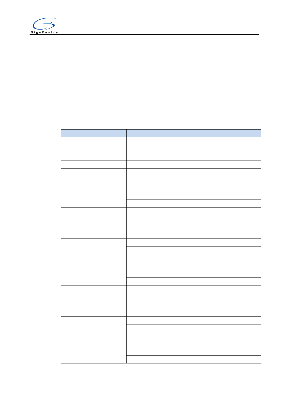
1 Summary
GD32450I-EVAL uses GD32F450IGH6 as the main controller. It uses Mini USB interface
or DC-005 connector to supply 5V power. SWD, Reset, Boot, User button key, LED,
CAN, I2C, I2S, USART, RTC, LCD, SPI, ADC, DAC, EXMC, CTC, SDIO, DCI, ENET,
USBFS, USBHS, GD-Link and Extension Pins are also included. For more details
please refer to GD32450I-EVAL-V1.1 schematic.
2 Function Pin Assign
Table 1 Function pin assign
4/ 51
Page 6

User Manual
PD6
EXMC_NWAIT
PD7
EXMC_NCE1
PD11
EXMC_CLE
PD12
EXMC_ALE
PD14
EXMC_D0
PD15
EXMC_D1
PE7
EXMC_D4
PE8
EXMC_D5
PE9
EXMC_D6
PE10
EXMC_D7
SDRAM
PC2
EXMC_SDNE0
PC5
EXMC_SDCKE0
PD0
EXMC_D2
PD1
EXMC_D3
PD8
EXMC_D13
PD9
EXMC_D14
PD10
EXMC_D15
PD14
EXMC_D0
PD15
EXMC_D1
PE0
EXMC_NBL0
PE1
EXMC_NBL1
PE7
EXMC_D4
PE8
EXMC_D5
PE9
EXMC_D6
PE10
EXMC_D7
PE11
EXMC_D8
PE12
EXMC_D9
PE13
EXMC_D10
PE14
EXMC_D11
PE15
EXMC_D12
PF0
EXMC_A0
PF1
EXMC_A1
PF2
EXMC_A2
PF3
EXMC_A3
PF4
EXMC_A4
PF5
EXMC_A5
PF11
EXMC_NRAS
PF12
EXMC_A6
PF13
EXMC_A7
PF14
EXMC_A8
PF15
EXMC_A9
PG0
EXMC_A10
GD32450I-EVAL
5/ 51
Page 7
User Manual
PG1
EXMC_A11
PG2
EXMC_A12
PG4
EXMC_A14
PG5
EXMC_A15
PG8
EXMC_SDCLK
PG15
EXMC_NCAS
PH5
EXMC_SDNWE
SDIO
PD2
SDIO_CMD
PC12
SDIO_CK
PC8
SDIO_D0
PC9
SDIO_D1
PC10
SDIO_D2
PC11
SDIO_D3
DCI
PB6
DCI_I2C0_SCL
PB7
DCI_I2C0_SDA
PA4
DCI_HSYNC
PG9
DCI_VSYNC
PA6
DCI_PIXCLK
PA8
DCI_XCLK
PB9
DCI_D7
PB8
DCI_D6
PD3
DCI_D5
PC11
DCI_D4
PC9
DCI_D3
PC8
DCI_D2
PC7
DCI_D1
PC6
DCI_D0
LCD
PI3
LCD_Touch_PENIRQ
PF9
LCD_SPI4_MOSI
PF8
LCD_SPI4_MISO
PF7
LCD_SPI4_SCK
PF6
LCD_SPI4_NSS
PB15
LCD_PWM_BackLight
PH7
LCD_Touch_Busy
PH2
LCD_R0
PH3
LCD_R1
PH8
LCD_R2
PH9
LCD_R3
PH10
LCD_R4
PH11
LCD_R5
PH12
LCD_R6
PG6
LCD_R7
GD32450I-EVAL
6/ 51
Page 8
User Manual
PE5
LCD_G0
PE6
LCD_G1
PH13
LCD_G2
PH14
LCD_G3
PH15
LCD_G4
PI0
LCD_G5
PI1
LCD_G6
PI2
LCD_G7
PE4
LCD_B0
PG12
LCD_B1
PG10
LCD_B2
PG11
LCD_B3
PI4
LCD_B4
PI5
LCD_B5
PI6
LCD_B6
PI7
LCD_B7
PG7
LCD_CLK
PI10
LCD_HSYNC
PI9
LCD_VSYNC
Ethernet
PA1
ETH_RMII_REF_CLK
PA2
ETH_MDIO
PA7
ETH_RMII_CRS_DV
PG11
ETH_RMII_TX_EN
PG13
ETH_RMII_TXD0
PG14
ETH_RMII_TXD1
PC1
ETH_MDC
PC4
ETH_RMII_RXD0
PC5
ETH_RMII_RXD1
PA8
ETH_RMII_REF_CLK
USB_FS
PA9
USB_VBUS
PA11
USB_DM
PA12
USB_DP
USB_HS
PH4
USB_HS_ULPI_NXT
PI11
USB_HS_ULPI_DIR
PC0
USB_HS_ULPI_STP
PA5
USB_HS_ULPI_CK
PB5
USB_HS_ULPI_D7
PB13
USB_HS_ULPI_D6
PB12
USB_HS_ULPI_D5
PB11
USB_HS_ULPI_D4
PB10
USB_HS_ULPI_D3
PB1
USB_HS_ULPI_D2
GD32450I-EVAL
7/ 51
Page 9

User Manual
PB0
USB_HS_ULPI_D1
PA3
USB_HS_ULPI_D0
GD32450I-EVAL
3 Getting started
The EVAL board uses Mini USB connecter or DC-005 connector to get power DC +5V,
which is the hardware system normal work voltage. Three kinds of different USB power
supply which are USB_FS, USB_HS_ULPI, GD-Link can be chosen through JP4. A
J-Link tool or GD-Link on board is necessary in order to download and debug programs.
Select the correct boot mode and then power on, the LED5 will turn on, which indicates
that the power supply is OK.
There are Keil version and IAR version of all projects. Keil version of the projects are
created based on Keil MDK-ARM 4.74 uVision4. IAR version of the projects are created
based on IAR Embedded Workbench for ARM 7.40.2. In Firmware folder, Addon and
Software Pack are used to add the devices, peripherals and others to IDE. During use,
the following points should be noted:
1. If you use Keil uVision4 to open the project, install the GD32F4xx_Addon.1.0.0.exe
which is in \Library\Firmware to load the associated files.
2. If you use Keil uVision5 to open the project, there are two ways to solve the "Device
Missing (s)" problem. One is to install GigaDevice.GD32F4xx_DFP.1.0.0.pack which is
in \Library\Firmware. In Project menu, select the Manage sub menu, click on the
“Version Migrate 5 Format...” menu, the Keil uVision4 project will be converted to Keil
uVision5 project. Then add “C:\Keil_v5\ARM\Pack\ARM\CMSIS\4.2.0\CMSIS\Include” to
C/C++ in Option for Target. The other is to install Addon directly. Select the installation
directory of Keil uVision5 software, such as C:\Keil_v5, in Destination Folder of Folder
Selection. Select the corresponding device in Device of Option for Target and add
“C:\Keil_v5\ARM\Pack\ARM\CMSIS\4.2.0\CMSIS\Include” to C/C++ in Option for Target.
3. If you use IAR to open the project, install IAR_GD32F4xx_Addon.exe which is in
\Library\Firmware to load the associated files.
8/ 51
Page 10
User Manual
G
1
Vout
2
Vin
3
4
U2 AMS1086CD-3.3
E1
16V/10uF,AVX
C17
50V/0.1uF
C18
50V/0.1uF
+3V3
LED5
LED0603
R7
470Ω
1
TP1
TP +3V3
P1
SMD1812P150TF/24
5
S2
3
S
2
S1
1
4
SW1
SS12D07VG4
1
3
2
CN1
DC-005
GND
VCC
+5V
GND
E2
16V/10uF,AVX
POWER
V_USB_5V
R4
10KΩ
1
2
3
JP2
BOOT0
GND
R5
10KΩ
1
2
3
JP3
BOOT1
GND
BOOT0
PB2
+3V3
+3V3
BOOT1
BOOT1
BOOT0
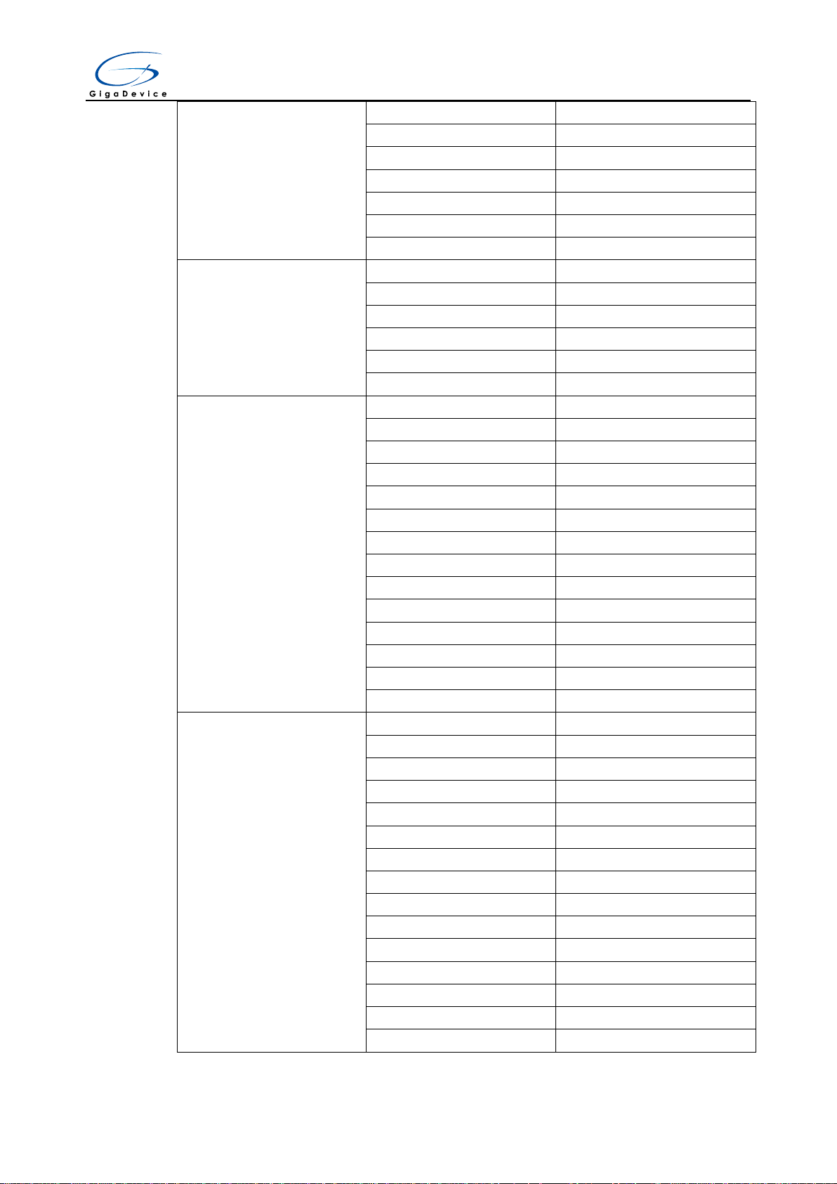
Boot Mode
Any
2-3
User memory
2-3
1-2
System memory
1-2
1-2
SRAM memory
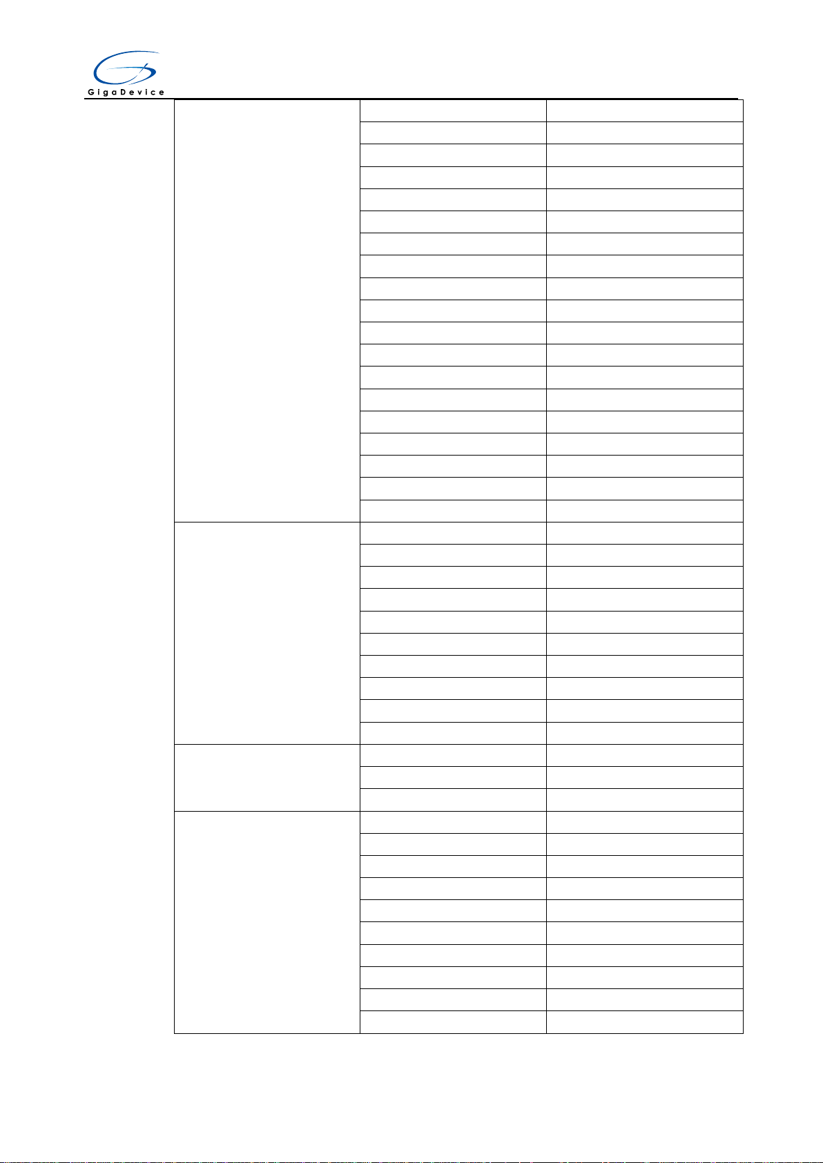
LED1
LED0603
LED2
LED0603
LED3
LED0603
R13
470Ω
R14
470Ω
R15
470Ω
LED
LED1
LED2
LED3
GND
PE2
PE3
PF10
GD32450I-EVAL
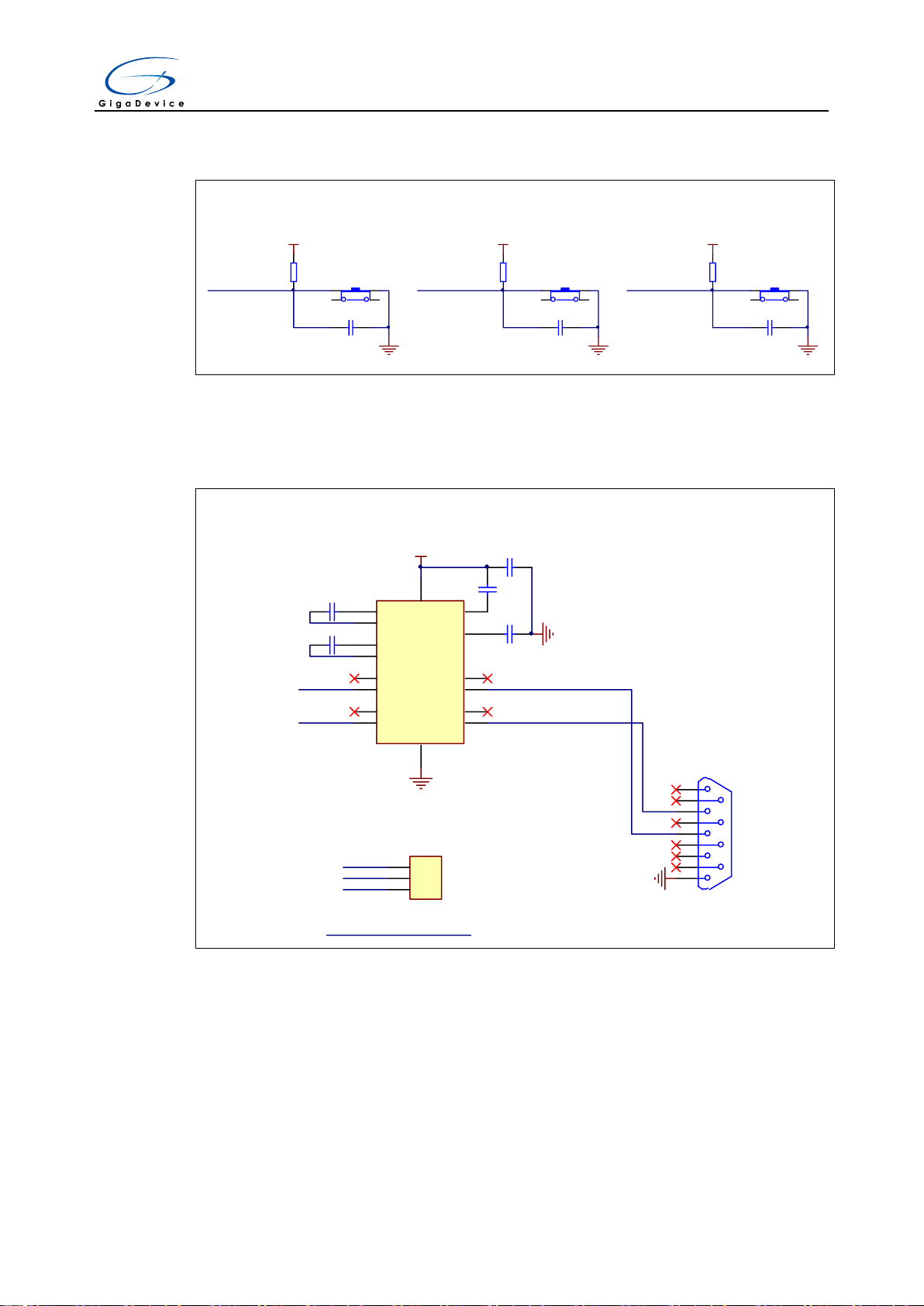
4 Hardware layout overview
4.1 Power
4.2 Boot
4.3 LED
9/ 51
Page 11
User Manual
KEY1
K2
K-1102B
R17
10KΩ
+3V3
GND
C28
50V/0.1uF
KEY2
K3
K-1102B
R18
10KΩ
+3V3
GND
C29
50V/0.1uF
KEY3
K4
K-1102B
R19
10KΩ
+3V3
GND
C30
50V/0.1uF
PA0 PC13 PB14
KEY
Wakeup Tamper USER
C1+
1
V+
2
C1-
3
C2+
4
C2-
5
V-
6
T2OUT
7
R2IN
8
R2OUT
9
T2IN
10
T1IN
11
R1OUT
12
R1IN
13
T1OUT
14
GND
15
VCC
16
U3
MAX3232CSE+
+3V3
GND
C23
50V/0.1uF
C25
50V/0.1uF
C24
50V/0.1uF
C22
50V/0.1uF
C21
50V/0.1uF
GND
USART0_TX
USART0_RX
USART0_TX
1
6
2
7
3
8
4
9
5
J1
COM1
GND
1
2
3
JP5
HEADER 3
PA9
PA10
USB_FS_VBUS
Short JP5(2,3)for USB_FS function
RS232_TX0
RS232_RX0
Short JP5(1,2)for USART0 function
USART0
USART0_RX
GD32450I-EVAL
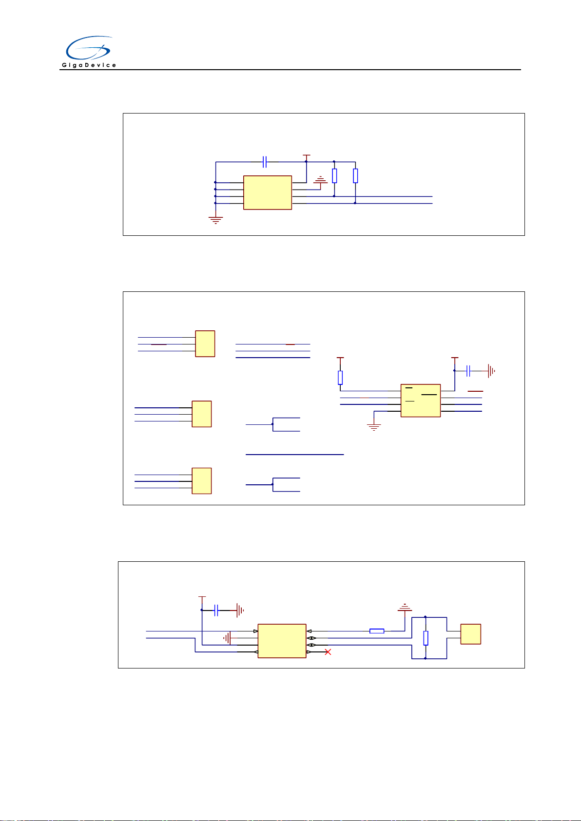
4.4 KEY
4.5 USART
10/ 51
Page 12
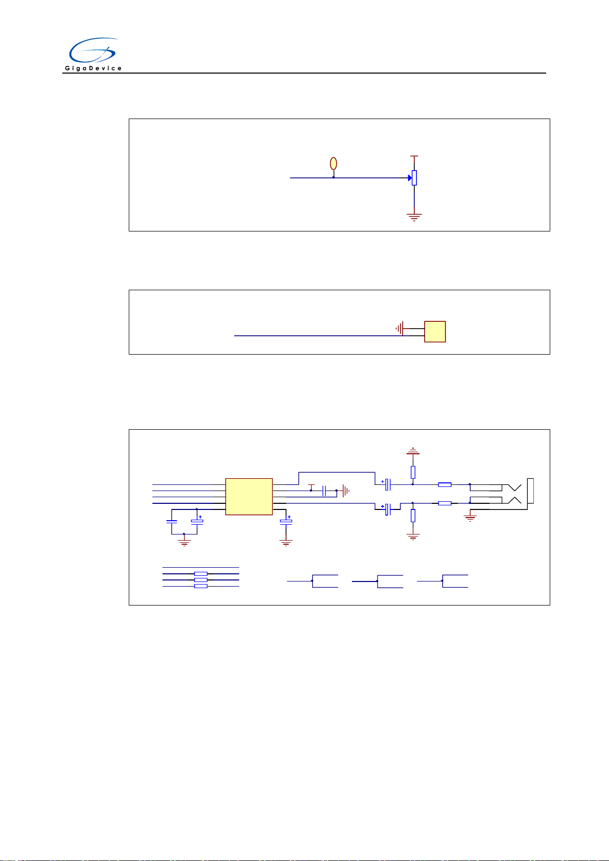
User Manual
+3V3
GND
ADC
PC3
VR1
10K
1
TP2
TP ADin
ADC012_IN13
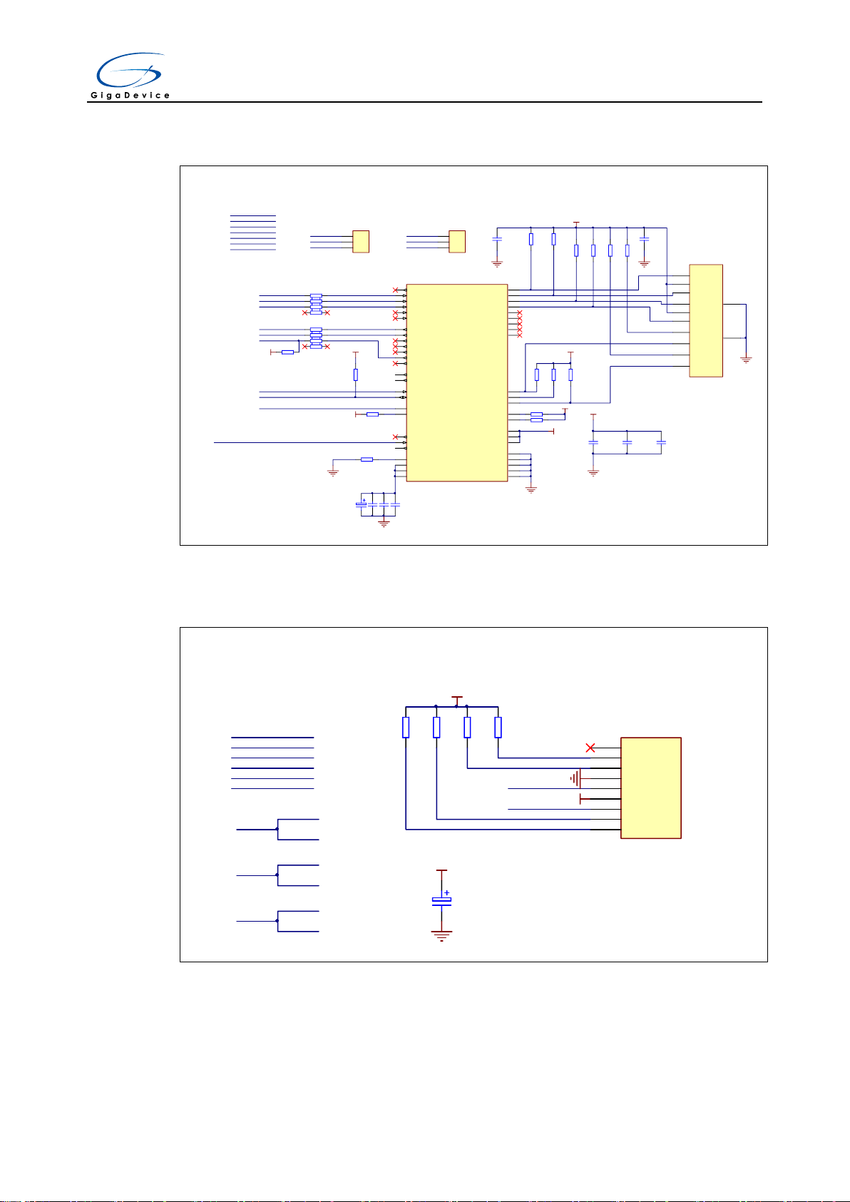
DAC
DAC_OUT0
GND
1
2
JP7
DAC
PA4
PA4 is an AFIO, please refer to DCI Schematic for right config
PC1 is an AFIO, please refer to ETHNET Schematic for right config
Pi1
Pi0
I2S1_SD
I2S1_CK
I2S1_WS
I2S1_MCKPA6
PC1
Pi1
LCD_G6
I2S1_CK
Pi0
LCD_G5
I2S1_WS
PA6
DCI_PIXCLK
I2S1_MCK
R43
0Ω
R44
0Ω
R55
0Ω
I2S
I2S1_MCK
I2S1_WS
I2S1_CK
I2S1_SD
C27
50V/0.1uF
GND
E7
16V/10uF,AVX
C34
50V/0.1uF
GND
E8
16V/10uF,AVX
GND
5
4
3
2
1
J2
HeadPhone
E4
16V/3.3uF,AVX
E6
16V/3.3uF,AVX
GND
R91
10KΩ
R24
10KΩ
GND
GND
R25
470Ω
R54
470Ω
SDIN
1
SCLK
2
LRCK
3
MCLK
4
VQ5FILT+
6
AOUTL
7
GND
8
AOUTR
10
VA
9
U7
CS4344
+3V3
GD32450I-EVAL
4.6 ADC
4.7 DAC
4.8 I2S
11/ 51
Page 13
User Manual
A0
1
A1
2
A2
3
GND
4
SDA
5
SCL
6
WP
7
VCC
8
U4
AT24C02C-SSHM-T
+3V3
GND
R10
4.7KΩ
R11
4.7KΩ
I2C0_SCL
I2C0_SDA
I2C
C26
50V/0.1uF
GND
PB7
PB6
CS
1
SO
2
WP
3
GND4SI
5
SCLK
6
HOLD
7
VCC
8
U5
GD25Q16BS
+3V3
GND
SPIFlash_CS
R21
10KΩ
+3V3
C32
50V/0.1uF
GND
SPI5_MISO_IO1
SPI5_WP_IO2
SPI5_MOSI_IO0
SPI5_SCK
SPI5_HOLD_IO3
Standard & Quad SPI Flash
SPI5_MOSI_IO0
SPI5_MISO_IO1
SPI5_WP_IO2SPI5_HOLD_IO3
SPI5_SCK
SPIFlash_CS
PG14
PG12
PG10
PG11
PG13
Pi8
1
2
3
JP12
HEADER 3
1
2
3
JP13
HEADER 3
1
2
3
JP20
HEADER 3
RMII_TX_EN
RMII_TXD0
RMII_TXD1
Short JP12(1,2) for Ethnet function
Short JP12(2,3) for SPI & TLI function
Short JP13(1,2) for Ethnet function
Short JP13(2,3) for SPI function
Short JP20(1,2) for Ethnet function
Short JP20(2,3) for SPI function
PG10
SPI5_#WP_IO2
LCD_B2
SPI5_#HOLD_IO3
PG12
SPI5_MISO_IO1
LCD_B1
LCD_B3
D
1
GND
2
VCC
3
R
4
Vref
5
CANL
6
CANH
7
RS
8
U6
SN65HVD230
CAN0H
CAN0L
R22
0Ω
GND
R23
120Ω
1
2
JP14
HEADER 2
CAN0_TX
CAN0_RX
GND
+3V3
C33
50V/0.1uF
GND
CAN
PB9
PB8
GD32450I-EVAL
4.9 I2C
4.10 SPI
4.11 CAN
12/ 51
Page 14
User Manual
TX_CLK
1
TX_EN
2
TXD_0
3
TXD_1
4
TXD_2
5
TXD_3/SNI_MODE
6
PWR_DOWN/INT
7
NC
8
NC
9
NC
10
NC
11
NC
12
RD-
13
RD+
14
AGND
15
TD-
16
TD+
17
PFBIN1
18
AGND
19
NC
20
NC
21
AVDD33
22
PFBOUT
23
RBIAS
24
25MHz_OUT
25
LED_ACT/COL/AN_EN
26
LED_SPEED/AN1
27
LED_LINK/AN0
28
RESET_N
29
MDIO
30
MDC
31
IOVDD33
32
X2
33
X1
34
IOGND
35
DGND
36
PFBIN2
37
RX_CLK
38
RX_DV/MII_MODE
39
CRS/CRS_DV/LED_CFG
40
RX_ER/MDIX_EN
41
COL/PHYAD0
42
RXD_0/PHYAD1
43
RXD_1/PHYAD2
44
RXD_2/PHYAD3
45
RXD_3/PHYAD4
46
IOGND
47
IOVDD33
48
U8
DP83848CVV
+3V3
R32
2.2KΩ
RMII MODE
R33
1.5KΩ
+3V3
NRST
R40
2.2KΩ
+3V3
R41
4.87KΩ
GND
E3
16V/10uF,AVX
C37
50V/0.1uF
C38
50V/0.1uF
C39
50V/0.1uF
GND
GND
+3V3
R38
2.2KΩ
R39
2.2KΩ
+3V3
R34
2.2KΩ
R35
2.2KΩ
R36
2.2KΩ
+3V3
TD+
1
4
TD-
2
RD+
3
5
RD-
6
L+
9
L-
10
R+
12
R-
11
GND1
13
GND2
14
JP16
HR911105A
GND
+3V3
R26
49.9Ω
R27
49.9Ω
R28
49.9Ω
R29
49.9Ω
C36
50V/0.1uF
C35
50V/0.1uF
GND GND
R30
240Ω
R31
240Ω
C40
50V/0.1uF
C41
50V/0.1uF
C42
50V/0.1uF
+3V3
GND
PC4
PC5
PA1
MCO
RMII_TX_EN
RMII_TXD0
RMII_TXD1
RMII_RXD0
RMII_RXD1
RMII_CRS_DV
RMII_MDC
RMII_MDIO
RMII_REF_CLK
RMII_TX_EN
RMII_TXD0
RMII_TXD1
RMII_RXD0
RMII_RXD1
RMII_MDC
RMII_MDIO
RMII_REF_CLK
RMII_CRS_DV
RP2
33Ω
RP3
33Ω
PA8
PA8 is an AFIO, refer to DCI schematic for right config
Ethernet
PA7
PA2
PG11
PG13
PG14
PG11、PG13、PG14 are AFIOs, please refer to SPI schematic for right config
1
2
3
JP17
HEADER 3
EXMC_SDCKE0
Short JP17(1,2) for Ethnet function
Short JP17(2,3) for SDRAM function
PC1
1
2
3
JP18
HEADER 3
Short JP18(1,2) for Ethnet function
Short JP18(2,3) for I2S function
I2S1_SD
R37
10KΩ
R42
10KΩ
R45
10KΩ
R46
10KΩ
+3V3
+3V3
E5
16V/10uF,AVX
GND
PD2
PC12
SDIO_DAT3
SDIO_CMD
SDIO_CLK
SDIO_DAT0
SDIO_DAT1
SDIO_DAT3
SDIO_CMD
SDIO_CLK
SDIO_DAT0
SDIO_DAT1
SDIO_DAT2
D2
1
D3
2
CMD
3
VCC
4
CLK
5
GND
6
D0
7
D1
8
CD
9
JP32
TF_CARD_SOCKET
+3V3
SDIO
GND
SDIO_DAT2PC10
PC8
PC9
PC11
PC8
SDIO_DAT0
DCI_D2
PC9
SDIO_DAT1
DCI_D3
PC11
SDIO_DAT2
DCI_D4
GD32450I-EVAL
4.12 Ethernet
4.13 SDIO
13/ 51
Page 15

User Manual
EXMC_D0
EXMC_D1
EXMC_D2
EXMC_D3
EXMC_D4
EXMC_D5
EXMC_D6
EXMC_D7
EXMC_NWE
EXMC_NOE
PD14
PD15
PE7
PE8
PE9
PE10
PD4
CL
16
AL
17
W
18
R
8
E
9
VSS2
36
VSS1
13
VDD2
37
VDD1
12
IO7
44
IO6
43
IO5
42
IO4
41
IO3
32
IO2
31
IO1
30
IO0
29
WP
19
RB
7
U11
HY27UF081G2A
EXMC_A16
EXMC_A17
EXMC_NWE
EXMC_NOE
R64
10KΩ
+3V3
R63
10KΩ
+3V3
R66
10KΩ
+3V3
EXMC_NWAIT
GND
+3V3
Nand Flash
EXMC_D7
EXMC_D6
EXMC_D5
EXMC_D4
EXMC_D3
EXMC_D2
EXMC_D1
EXMC_D0
C50
50V/0.1uF
C51
50V/0.1uF
+3V3
GND
EXMC_A17
EXMC_A16
EXMC_NWAIT
EXMC_NCE1
PD11
PD12
PD7
EXMC_NCE1
PD5
PD6
PD0
PD1
VDD
1
DQ0
2
VDDQ
3
DQ1
4
DQ2
5
VSSQ
6
DQ3
7
DQ4
8
VDDQ
9
DQ5
10
DQ6
11
VSSQ
12
DQ7
13
VDD
14
LDQM
15
WE
16
CAS
17
RAS
18
CS
19
BA0
20
BA1
21
A10/AP
22
A0
23
A1
24
A2
25
A3
26
VDD
27
VSS
28
A4
29
A5
30
A6
31
A7
32
A8
33
A9
34
A11
35
A12
36
CKE
37
CLK
38
UDQM
39
NC
40
VSS
41
DQ8
42
VDDQ
43
DQ9
44
DQ10
45
VSSQ
46
DQ11
47
DQ12
48
VDDQ
49
DQ13
50
DQ14
51
VSSQ
52
DQ15
53
VSS
54
U9
MT48LC16M16A2P-6AIT
+3V3
GND
+3V3
+3V3
+3V3
+3V3
+3V3GND
GND
GND
GND
GND
GND
GND
EXMC_D0
EXMC_D1
EXMC_D2
EXMC_D3
EXMC_D4
EXMC_D5
EXMC_D6
EXMC_D7 EXMC_D8
EXMC_D9
EXMC_D10
EXMC_D11
EXMC_D12
EXMC_D13
EXMC_D14
EXMC_D15
EXMC_NBL0
EXMC_NBL1EXMC_SDNWE
EXMC_SDNCAS
EXMC_SDNRAS
EXMC_SDNE0
EXMC_BA0
EXMC_BA1
EXMC_A0
EXMC_A1
EXMC_A2
EXMC_A3 EXMC_A4
EXMC_A5
EXMC_A6
EXMC_A7
EXMC_A8
EXMC_A9
EXMC_A10
EXMC_A11
EXMC_A12
EXMC_SDCKE0
EXMC_SDCLK
EXMC_D0
PE11
PE12
PE13
PE14
PE15
PD8
PD9
PD10
+3V3
+3V3
PH5
PC2
EXMC_SDNWE
EXMC_SDNE0
EXMC_SDCKE0
PE0
PE1
PF0
PF1
PF2
PF3
PF4
PF5
PF14
PF15
PF11
PF12
PF13
PG0
PG1
PG2
PG4
PG5
PG15
PG8
EXMC_NBL0
EXMC_NBL1
EXMC_SDNCAS
EXMC_SDNRAS
EXMC_BA0
EXMC_BA1
EXMC_SDCLK
EXMC_A0
EXMC_D1
EXMC_D2
EXMC_D3
EXMC_D4
EXMC_D5
EXMC_D6
EXMC_D7
EXMC_D8
EXMC_D9
EXMC_D10
EXMC_D11
EXMC_D12
EXMC_D13
EXMC_D14
EXMC_D15
EXMC_A1
EXMC_A2
EXMC_A3
EXMC_A4
EXMC_A5
EXMC_A6
EXMC_A7
EXMC_A8
EXMC_A9
EXMC_A10
EXMC_A11
EXMC_A12
SDRAM
DCI_8bit, TLI and SDRAM can be used at the same time
C52
50V/0.1uF
C53
50V/0.1uF
C54
50V/0.1uF
C55
50V/0.1uF
C56
50V/0.1uF
C57
50V/0.1uF
C58
50V/0.1uF
PD0
PD1
PE7
PE8
PE9
PE10
PD14
PD15
R8
10KΩ
PC5
PC5 is AFIO, please refer to ETHNET schematic for right config
GD32450I-EVAL
4.14 NAND Flash
4.15 SDRAM
14/ 51
Page 16
User Manual
DCI 8bit
+3V3
DCI_I2C0_SCL
DCI_VSYNC
DCI_PIXCLK
DCI_D7
DCI_D5
DCI_D3
DCI_D1
GND
DCI_I2C0_SDA
DCI_HSYNC
DCI_XCLK
DCI_D6
DCI_D4
DCI_D2
DCI_D0
DCI_I2C0_SCL
DCI_I2C0_SDA
DCI_VSYNC
DCI_HSYNC
DCI_PIXCLK
DCI_XCLK
DCI_D5
DCI_D4
DCI_D3
DCI_D2
DCI_D1
DCI_D0
PG9
PA6
PA8
PC6
PC7
PC8
PC9
PC11
PD3
DCI_8bit, TLI and SDRAM can be used at the same time
1
2
3
JP22
HEADER 3
Short JP22(1,2) for Ethnet function
Short JP22(2,3) for DCI function
RMII_REF_CLK
PB9
PB8
1
2
3
JP19
HEADER 3
1
2
3
JP21
HEADER 3
CAN0_TX
CAN0_RX
Short JP19(1,2) for CAN function
DCI_D6
DCI_D7
Short JP19(2,3) for DCI function
Short JP21(1,2) for CAN function
Short JP21(2,3) for DCI function
OV2640
PB7
PB6
PA4
1
2
3
JP23
HEADER 3
Short JP23(1,2) for DAC function
Short JP23(2,3) for DCI function
DAC_OUT0
R20
0Ω
R16
0Ω
R12
0Ω
PC8
SDIO_DAT0
DCI_D2
PC9
SDIO_DAT1
DCI_D3
PC11
SDIO_DAT2
DCI_D4
1 2
3 4
5 6
7 8
9 10
11 12
13 14
15 16
JP27
8×2P2.54
PA6
DCI_PIXCLK
I2S1_MCK
TLI
PG12
PG10
PE4
Pi5
Pi4
Pi6
Pi7
LCD_B1
LCD_B2
LCD_B3
LCD_B4
LCD_B5
LCD_B6
LCD_B7
LCD_B0
PE5
PE6
PH13
Pi2
PH15
Pi0
Pi1
PH14
LCD_G0
LCD_G1
LCD_G2
LCD_G3
LCD_G4
LCD_G5
LCD_G6
LCD_G7
PH9
PH12
PG6
PH3
PH2
PH10
PH11
PH8
LCD_R0
LCD_R1
LCD_R2
LCD_R3
LCD_R4
LCD_R5
LCD_R6
LCD_R7
PG7
Pi10
Pi9
LCD_CLK
LCD_HSYNC
LCD_VSYNC
LCD_SPI4_NSS
LCD_SPI4_SCK
LCD_SPI4_MISO
LCD_SPI4_MOSI
PH7
LCD_Touch_PENIRQ
LCD_PWM_BackLight
LCD_Touch_Busy
1 2
3 4
5 6
7 8
9 10
11 12
13 14
15 16
17 18
19 20
21 22
23 24
25 26
27 28
29 30
31 32
33 34
35 36
37 38
39 40
JP30
20X2P2.54
LCD_Touch_PENIRQ
+5V
LCD_SPI4_MOSI
LCD_SPI4_SCK
LCD_PWM_BackLight
LCD_Touch_Busy
LCD_R0 LCD_R1
LCD_R2 LCD_R3
LCD_R4 LCD_R5
LCD_R6 LCD_R7
LCD_G0 LCD_G1
LCD_G2 LCD_G3
LCD_G4 LCD_G5
LCD_G6 LCD_G7
LCD_B0 LCD_B1
LCD_B2 LCD_B3
LCD_B4 LCD_B5
LCD_B6 LCD_B7
LCD_CLK
LCD_HSYNC
LCD_SPI4_MISO
LCD_SPI4_NSS
GND
LCD_VSYNC
GND
DCI_8bit, TLI and SDRAM can be used at the same time
R117
0Ω
R118
0Ω
R119
0Ω
SPI5_HOLD_IO3PG11
PG10
SPI5_#WP_IO2
LCD_B2
PG12
SPI5_MISO_IO1
LCD_B1
LCD_DE
GND
PG10、PG11、PG12 are AFIO, please refer to SPI Schematic for right config
Pi3
PB15
PF7
PF9
PF8
PF6
Pi1
LCD_G6
I2S1_CK
Pi0
LCD_G5
I2S1_WS
GD32450I-EVAL
4.16 DCI
4.17 LCD
15/ 51
Page 17

User Manual
GND
R58
22Ω
R59
22Ω
E10
16V/10uF,AVX
GND
PA11
PA12
R62
1MΩ
C49
50V/4.7nF
USB_FS_VBUS
USB_FS_DM
USB_FS_DP
VBUS
1
DM
2
DP
3
ID
4
GND
5
Shield
6
USB_MiniAB receptacle
CN2
Mini_USB
PA9
PA9 is AFIO, please refer to USART schematic for right config
GND
VBUS_FS_5V
R120
10KΩ
"VBUS_FS_5V control( active HIGH)" see USB_HS schematic
PD13---->
USB_HS_ULPI_D0
GND
1
GND
2
CPEN
3
VBUS
4
ID
5
VDD3.3
6
DP
7
DM
8
RESET
9
EXTVBUS
10
NXT
11
DIR
12
STP
13
CLKOUT
14
VDD1.8
15
VDD3.3
16
D7
17
D6
18
D5
19
D4
20
D3
21
D2
22
D1
23
D0
24
VDD3.3
25
VDD1.8
26
XO
27
XI
28
VDDA1.8
29
VDD3.3
30
REG_EN
31
RBIAS
32
GNDPAD
33
U13
USB3300-EZK
R98
10KΩ
R111
12KΩ
GND
VBUS
1
DM
2
DP
3
ID
4
GND
5
Shield
6
USB_MiniAB receptacle
CN3
Mini_USB
R114
1MΩ
C70
50V/4.7nF
GND
GND
R112
820Ω
+5V
GND
C64
50V/0.1uF
C65
50V/0.1uF
C66
50V/0.1uF
C67
50V/0.1uF
GND
+3V3
E13
16V/4.7uF,AVX
E12
16V/4.7uF,AVX
C71
50V/0.1uF
GND
C69
50V/0.1uF
GND
GND
R116
10KΩ
GND
USB_HS_ULPI_D1
USB_HS_ULPI_D2
USB_HS_ULPI_D3
USB_HS_ULPI_D4
USB_HS_ULPI_D5
USB_HS_ULPI_D6
USB_HS_ULPI_D7
R113
33Ω
USB_HS_ULPI_DIR
USB_HS_ULPI_STP
USB_HS_ULPI_NXT
USB_HS_ULPI_CK
PH4
Pi11
PC0
PA5
PB5
PB13
PB12
PB11
PB10
PB1
PB0
PA3
C68
50V/20pF
C72
50V/20pF
Y3
SMT5032-24MHz
GND
R115
1MΩ
USB_HS_ULPI
ENA
1
FLGA
2
FLGB
3
ENB
4
OUTB
5
GND
6
IN
7
OUTA
8
U12
SP2526A-1EN
+3V3
LED6
LED RED
R99
470Ω
R100
10KΩ
GND
C63
50V/0.1uF
E11
16V/10uF,AVX
VBUS_HS_5V
PD13
VBUS_FS_5V
R96
10KΩ
GND
R97
10KΩ
ENA and ENB active HIGH
GD32450I-EVAL
4.18 USBFS
4.19 USBHS
16/ 51
Page 18

User Manual
Extension Pin
PE2
PE4
PE6
PC13
PC15
Pi9
OSC_IN
NRST
PE3
PE5
PC14
Pi10
OSC_OUT
Pi11
GND
GND
GND
GND
GND
PH12
GND
GND
GND
1 2
3 4
5 6
7 8
9 10
11 12
13 14
15 16
17 18
19 20
21 22
23 24
25 26
27 28
29 30
31 32
33 34
35 36
37 38
39 40
41 42
43 44
JP8
22X2P2.0
1 2
3 4
5 6
7 8
9 10
11 12
13 14
15 16
17 18
19 20
21 22
23 24
25 26
27 28
29 30
31 32
33 34
35 36
37 38
39 40
41 42
43 44
JP9
22X2P2.0
1 2
3 4
5 6
7 8
9 10
11 12
13 14
15 16
17 18
19 20
21 22
23 24
25 26
27 28
29 30
31 32
33 34
35 36
37 38
39 40
41 42
43 44
JP10
22X2P2.0
Pi8
PF0
PF1 PF2
PF3 PF4
PF5
GND
PF6
PF7 PF8
PF9 PF10
PC0
PC1 PC2
PC3
PA0
PA1 PA2
PH2 PH3
PH4 PH5
PA3
PA4
PA5 PA6
PA7 PC4
PC5 PB0
PB1 PB2
PF11 PF12
PF13 PF14
PF15 PG0
PG1 PE7
PE8 PE9
PE10 PE11
PE12 PE13
PE14 PE15
PB10 PB11
PH6 PH7
PH8 PH9
PH10 PH11
PB12
PB13 PB14
PB15 PD8
PD9 PD10
PD11 PD12
PD13
PD14
PD15 PG2
PG3 PG4
PG5 PG6
PG7 PG8
PC6 PC7
PC8 PC9
PA8 PA9
PA10 PA11
PA12 PA13
GND
PH13
PH14 PH15
Pi0 Pi1
NC
Pi2
BOOT0
GND
GND
GND
1 2
3 4
5 6
7 8
9 10
11 12
13 14
15 16
17 18
19 20
21 22
23 24
25 26
27 28
29 30
31 32
33 34
35 36
37 38
39 40
41 42
43 44
JP11
22X2P2.0
Pi3
GND
PA14 PA15
PC10 PC11
PC12 PD0
PD1 PD2
PD3 PD4
PD5
PD6
PD7 PG9
PG10 PG11
PG12 PG13
PG14
PG15
PB3 PB4
PB5 PB6
PB7
PB8 PB9
PE0 PE1
Pi4 Pi5
Pi6 Pi7
+3V3
+3V3
VBAT
+3V3
+3V3
+3V3
+3V3
+3V3
GND
GND
+3V3
+3V3
NC
NC
NC
NC
NC
NC
NC
L_USB_Ctr
C100
50V/20pF
C102
50V/20pF
Y101
HC-49S-8MHz
GND
L_NRST
+3V3
GND
R102
10KΩ
C103
50V/0.1uF
R104
10KΩ
GND
C105
50V/0.1uF
C106
50V/0.1uF
C107
50V/0.1uF
C108
50V/0.1uF
R101
1MΩ
L_OSC_IN
L_OSC_OUT
L_OSC_IN
L_OSC_OUT
L_NRST
GND
+3V3
GND
1
2
3
4
JP100
4×1P2.54
+3V3
GND
MCU SWD
HSE
Reset
L_TMS/IO
L_TDI
L_TDO/SWO
L_TCK/CLK
L_USB_DP
L_SWDIO
L_SWDCK
L_SWDIO
L_SWDCK
+3V3
L_USB_DM
BOOT0
44
NRST
7
OSC_IN/PD0
5
OSC_OUT/PD1
6
PA0-WKUP
10
PA1
11
PA2
12
PA3
13
PA4
14
PA5
15
PA6
16
PA7
17
PA8
29
PA9
30
PA10
31
PA11
32
PA12
33
PA13/JTMS/SWDIO
34
PA14/JTCK/SWCLK
37
PA15/JTDI
38
PB0
18
PB1
19
PB2/BOOT1
20
PB3/JTDO
39
PB4/JNTRST
40
PB5
41
PB6
42
PB7
43
PB8
45
PB9
46
PB10
21
PB11
22
PB12
25
PB13
26
PB14
27
PB15
28
PC13-TAMPER-RTC
2
PC14-OSC32_IN
3
PC15-OSC32_OUT
4
VBAT
1
VDD_1
24
VDD_2
36
VDD_3
48
VDDA
9
VSS_1
23
VSS_2
35
VSS_3
47
VSSA
8
U0
GD32F103C8T6
L_TReset
L_LED1
L_LED2
L_LED1 LED0603
L_LED2 LED0603
R103
10KΩ
GND
R109
1KΩ
R110
1KΩ
GND
GND
R105
22Ω
R106
22Ω
R108
1MΩ
C104
50V/4.7nF
L_USB_DM
L_USB_DP
GND
R107
1.5KΩ
L_USB_Ctr
VCC
1
D-
2
D+
3
ID
4
GND
5
SHELL
6
CN100
Mini_USB
PA15
PA13
PA14
PB3
L_TMS/IO
L_TCK/CLK
L_TDO/SWO
L_TDI
L_TReset NRST
GDLINK_5V
GD32450I-EVAL
4.20 Extension
4.21 GD-Link
5 Routine use guide
5.1 GPIO_Runing_Led
5.1.1 DEMO Purpose
This demo includes the following functions of GD32 MCU:
Learn to use GPIO control the LED
Learn to use SysTick to generate 1ms delay
GD32450I-EVAL board has three LEDs. The LED1, LED2 and LED3 are controlled by
GPIO. This demo will show how to light the LEDs.
17/ 51
Page 19

User Manual
GD32450I-EVAL
5.1.2 DEMO Running Result
Download the program <01_GPIO_Runing_Led> to the EVAL board, LED1, LED2,
LED3 will turn on in sequence with interval of 200ms, and turn off together, 200ms later,
repeat the process.
5.2 GPIO_Keyboard_Polling_mode
5.2.1 DEMO Purpose
This demo includes the following functions of GD32 MCU:
Learn to use GPIO control the LED and the KEY
Learn to use SysTick to generate 1ms delay
GD32450I-EVAL board has four keys and three LEDs. The four keys are Reset key,
Tamper key, Wakeup key and User key. The LED1, LED2 and LED3 are controlled by
GPIO.
This demo will show how to use the Tamper key to control the LED1.When press down
the Tamper Key, it will check the input value of the IO port. If the value is 0 and will wait
for 100ms.Check the input value of the IO port again. If the value still is 0, it indicates
that the button is pressed successfully and toggle LED1.
5.2.2 DEMO Running Result
Download the program <02_GPIO_KeyBoard_Polling_mode> to the EVAL board, press
down the Tamper Key, LED1 will be turned on. Press down the Tamper Key again, LED1
will be turned off.
5.3 GPIO_KeyBoard_Interrupt_mode
5.3.1 DEMO Purpose
This demo includes the following functions of GD32 MCU:
Learn to use GPIO control the LED and the KEY
Learn to use EXTI to generate external interrupt
GD32450I-EVAL board has four keys and three LEDs. The four keys are Reset key,
Tamper key, Wakeup key and User key. The LED1, LED2 and LED3 are controlled by
GPIO.
18/ 51
Page 20

User Manual
GD32450I-EVAL
This demo will show how to use the EXTI interrupt line to control the LED1.When press
down the Tamper Key, it will produce an interrupt. In the interrupt service function, the
demo will toggle LED1.
5.3.2 DEMO Running Result
Download the program <03_GPIO_KeyBoard_Interrupt_mode> to the EVAL board,
Press down the Tamper Key, LED1 will be turned on. Press down the Tamper Key again,
LED1 will be turned off.
5.4 USART_Printf
5.4.1 DEMO Purpose
This demo includes the following functions of GD32 MCU:
Learn to use GPIO control the LED
Learn to retarget the C library printf function to the USART
5.4.2 DEMO Running Result
Download the program < 04_USART_Printf > to the EVAL board, jump the JP5 to
USART with the jumper cap and connect serial cable to EVAL_COM1. This
implementation outputs “USART printf example: please press the Tamper key” on the
HyperTerminal using EVAL_COM1. Press the Tamper key, serial port will output “USART
printf example”.
The output information via the serial port is as following.
5.5 USART_Echo_Interrupt_mode
5.5.1 DEMO Purpose
This demo includes the following functions of GD32 MCU:
Learn to use the USART transmit and receive interrupts to communicate with the
serial terminal tool
19/ 51
Page 21

User Manual
GD32450I-EVAL
5.5.2 DEMO Running Result
Download the program < 05_USART_Echo_Interrupt_mode > to the EVAL board, jump
the JP5 to USART with the jumper cap and connect serial cable to EVAL_COM1. Firstly,
all the LEDs are turned on and off for test. Then, the EVAL_COM1 sends the tx_buffer
array (from 0x00 to 0xFF) to the serial terminal tool supporting hex format
communication and waits for receiving data of BUFFER_SIZE bytes from the serial
terminal. The data MCU have received is stored in the rx_buffer array. After that,
compare tx_buffer with rx_buffer. If tx_buffer is same with rx_buffer, LED1, LED2, LED3
flash by turns. Otherwise, LED1, LED2, LED3 toggle together.
The output information via the serial port is as following.
5.6 USART_DMA
5.6.1 DEMO Purpose
This demo includes the following functions of GD32 MCU:
Learn to use the USART transmit and receive data using DMA
5.6.2 DEMO Running Result
Download the program < 06_USART_DMA > to the EVAL board, jump the JP5 to
USART with the jumper cap and connect serial cable to EVAL_COM1. Firstly, all the
LEDs are turned on and off for test. Then, the EVAL_COM1 sends the tx_buffer array
(from 0x00 to 0xFF) to the serial terminal tool supporting hex format communication and
waits for receiving data of same bytes as tx_buffer from the serial terminal. The data
MCU have received is stored in the rx_buffer array. After that, compare tx_buffer with
rx_buffer. If tx_buffer is same with rx_buffer, LED1, LED2, LED3 flash by turns.
Otherwise, LED1, LED2, LED3 toggle together.
20/ 51
Page 22

User Manual
GD32450I-EVAL
5.7 ADC_Temperature_Vrefint_Vbat
5.7.1 DEMO Purpose
This demo includes the following functions of GD32 MCU:
Learn to use the ADC to convert analog signal to digital data
Learn to get the value of inner channel 16(temperature sensor channel), channel 17
(VREFINT channel) and channel 18(VBAT/4 channel)
5.7.2 DEMO Running Result
Jump the JP5 to USART with the jumper cap, and then download the program
<07_ADC_Temperature_Vrefint_Vbat> to the GD32450I-EVAL board. Connect serial
cable to EVAL_COM1, open the HyperTerminal.
When the program is running, HyperTerminal display the value of temperature, internal
voltage reference (VREFINT) and external battery voltage V
Notice: because there is an offset, when inner temperature sensor is used to detect
accurate temperature, an external temperature sensor part should be used to calibrate
the offset error.
BAT
.
21/ 51
Page 23

User Manual
GD32450I-EVAL
5.8 ADC0_ADC1_Follow_up_mode
5.8.1 DEMO Purpose
This demo includes the following functions of GD32 MCU:
Learn to use the ADC to convert analog signal to digital data
Learn to use ADC0 and ADC1 follow-up mode
5.8.2 DEMO Running Result
Jump the JP5 to USART with the jumper cap, and then download the program
<08_ADC0_ADC1_Follow_up_mode> to the GD32450I-EVAL board. Connect serial
cable to EVAL_COM1, open the HyperTerminal. PC5 pin connect to the external voltage
input. PC3 is the output voltage of the slide rheostat VR1 on board. Keep PC5 pin
should not be reused by other peripherals. JP17 should not be connected.
TIMER1_CH1 is the trigger source of ADC0 and ADC1. When the rising edge of
TIMER1_CH1 coming, ADC0 starts immediately and ADC1 starts after a delay of
several ADC clock cycles. The values of ADC0 and ADC1 are transmitted to array
adc_value[0] and adc_value [1] by DMA.
When the first rising edge of TIMER1_CH1 coming, the value of the ADC0 conversion of
PC3 pin is stored into the low half word of adc_value [0], and after a delay of several
ADC clock cycles the value of the ADC1 conversion of PC5 pin is stored into the high
half word of adc_value [0]. When the second rising edge of TIMER1_CH1 coming, the
value of the ADC0 conversion of PC5 pin is stored into the low half word of adc_value [1],
and after a delay of several ADC clock cycles the value of the ADC1 conversion of PC3
pin is stored into the high half word of adc_value [1].
When the program is running, HyperTerminal display the regular value of ADC0 and
ADC1 by adc_value [0] and adc_value [1].
22/ 51
Page 24

User Manual
GD32450I-EVAL
5.9 ADC0_ADC1_Regular_Parallel_mode
5.9.1 DEMO Purpose
This demo includes the following functions of GD32 MCU:
Learn to use the ADC to convert analog signal to digital data
Learn to use ADC0 and ADC1 regular parallel mode
5.9.2 DEMO Running Result
Jump the JP5 to USART with the jumper cap, and then download the program
<09_ADC0_ADC1_Regular_Parallel_mode> to the GD32450I-EVAL board. Connect
serial cable to EVAL_COM1, open the HyperTerminal. PC5 pin connect to the external
voltage input. PC3 is the output voltage of the slide rheostat VR1 on board. Keep PC5
pin should not be reused by other peripherals. JP17 should not be connected.
TIMER1_CH1 is the trigger source of ADC0 and ADC1. When the rising edge of
TIMER1_CH1 coming, ADC0 and ADC1 convert the regular channel group parallelly.
The values of ADC0 and ADC1 are transmitted to array adc_value[0] and adc_value [1]
by DMA.
When the first rising edge of TIMER1_CH1 coming, the value of the ADC0 conversion of
PC3 pin is stored into the low half word of adc_value [0], the value of the ADC1
conversion of PC5 pin is stored into the high half word of adc_value [0]. When the
second rising edge of TIMER1_CH1 coming, the value of the ADC0 conversion of PC5
pin is stored into the low half word of adc_value [1], the value of the ADC1 conversion of
PC3 pin is stored into the high half word of adc_value [1].
When the program is running, HyperTerminal displays the regular value of ADC0 and
23/ 51
Page 25

User Manual
GD32450I-EVAL
ADC1 stored in adc_value [0] and adc_value [1].
5.10 DAC_Output_Voltage_Value
5.10.1 DEMO Purpose
This demo includes the following functions of GD32 MCU:
Learn to use DAC to output voltage on DAC0 output
5.10.2 DEMO Running Result
Jump the JP23 to DAC with the jumper cap, download the program
<10_DAC_Output_Voltage_Value> to the EVAL board and run, all the LEDs will turn on
and turn off for test. The digital value is 0x7FF0, its converted analog voltage should be
1.65V(VREF/2), using the voltmeter to measure PA4 or JP7, its value is 1.65V.
5.11 I2C_EEPROM
5.11.1 DEMO Purpose
This demo includes the following functions of GD32 MCU:
Learn to use the master transmitting mode of I2C module
Learn to use the master receiving mode of I2C module
Learn to read and write the EEPROM with I2C interface
24/ 51
Page 26

User Manual
GD32450I-EVAL
5.11.2 DEMO Running Result
Jump the JP5 to USART with the jumper cap, and download the program
<11_I2C_EEPROM> to the EVAL board and run. Connect serial cable to COM1, and
open the HyperTerminal to show the print message.
Firstly, the data of 256 bytes will be written to the EEPROM from the address 0x00 and
printed by the serial port. Then, reading the EEPROM from address 0x00 for 256 bytes
and the result will be printed. Finally, compare the data that were written to the EEPROM
and the data that were read from the EEPROM. If they are the same, the serial port will
output "I2C-AT24C02 test passed!" and the three LEDs lights flashing, otherwise the
serial port will output "Err: data read and write aren't matching." and all the three LEDs
light.
The output information via the serial port is as following.
25/ 51
Page 27

User Manual
GD32450I-EVAL
5.12 SPI_QSPI_Flash
5.12.1 DEMO Purpose
This demo includes the following functions of GD32 MCU:
Learn to use the Quad-SPI mode of SPI unit to read and write NOR Flash with the
SPI interface
GD32450I-EVAL board integrates SPI5 module with Quad-SPI mode and the mode can
communicate with external NOR Flash devices. The SPI NOR FLASH is a serial FLASH
memory chip GD25Q16B which size is 16Mbit, the chip supports standard SPI and quad
SPI operation instructions.
5.12.2 DEMO Running Result
The computer serial port line connected to the COM1 port of development board, set the
baud rate of HyperTerminal software to 115200, 8 bits data bit, 1 bit stop bit. At the same
time you should jump the JP5 to USART, and jump the JP12,JP13,JP20 to SPI.
Download the program <12_SPI_QSPI_Flash> to the EVAL board, the HyperTerminal
software can observe the operation condition and will display the ID of the flash, 256
bytes data which are written to and read from flash. Compare the data that were written
to the flash and the data that were read from the flash. If they are the same, the serial
port will output “SPI-GD25Q16 Test Passed!”, otherwise, the serial port will output “Err:
Data Read and Write aren't Matching.”. At last, turn on and off the leds one by one. The
following is the experimental results.
26/ 51
Page 28

User Manual
GD32450I-EVAL
5.13 I2S_Audio_Player
5.13.1 DEMO Purpose
This Demo includes the following functions of GD32 MCU:
Learn to use I2S module to output audio file
Parsing audio files of wav format
GD32450I-EVAL board integrates the I2S(Inter-IC Sound) module, and the module can
communicate with external devices using the I2S audio protocol. This Demo mainly
shows how to use the I2S interface of the board for audio output.
5.13.2 DEMO Running Result
Download the program<13_I2S_Audio_Player>to the EVAL board, jump the JP18 to I2S
27/ 51
Page 29

User Manual
GD32450I-EVAL
with the jumper cap, insert the headphone into the audio port, and then listen to the
audio file.
5.14 EXMC_SDRAM
5.14.1 DEMO Purpose
This demo includes the following functions of GD32 MCU:
Learn to use EXMC control the SDRAM
5.14.2 DEMO Running Result
GD32450I-EVAL board has EXMC module to control SDRAM. Before running the demo,
JP17 must be fitted to SDRAM, JP5 must be fitted to USART. Download the program
<14_EXMC_SDRAM> to the EVAL board. This demo shows the write and read
operation process of SDRAM memory by EXMC module. If the test succeed, LED1 will
be turned on. Otherwise, turn on the LED3. Information via a HyperTerminal output as
following:
5.15 EXMC_SDRAM_DeepSleep
5.15.1 DEMO Purpose
This demo includes the following functions of GD32 MCU:
Learn to use EXMC control the SDRAM
Learn to use deepsleep mode
5.15.2 DEMO Running Result
GD32450I-EVAL board has EXMC module to control SDRAM. Before running the demo,
28/ 51
Page 30

User Manual
GD32450I-EVAL
JP17 must be fitted to SDRAM, JP5 must be fitted to USART. Download the program
<15_EXMC_SDRAM_DeepSleep> to the EVAL board. This demo shows how to use
SDRAM in the deepsleep mode. Firstly, MCU works in the normal mode, SDRAM
auto-refresh cycles are performed by MCU, we write the specified data to the SDRAM.
Secondly, we make the MCU to deepsleep mode, at the time, SDRAM auto-refresh
cycles are performed by itself and LED2 will light on. Thirdly, press the user key to wake
up MCU, compare the data which read from SDRAM with the write data, if the test pass,
LED1 will be turned on. Otherwise, turn on the LED3. Information via a HyperTerminal
output as following:
5.16 EXMC_NandFlash
5.16.1 DEMO Purpose
This demo includes the following functions of GD32 MCU:
Learn to use EXMC control the NAND flash
5.16.2 DEMO Running Result
GD32450I-EVAL board has EXMC module to control NAND flash. Before running the
demo, JP5 must be fitted to USART. Download the program <16_EXMC_NandFlash> to
the EVAL board. This demo shows the write and read operation process of NAND flash
memory by EXMC module. If the test pass, LED1 will be turned on. Otherwise, turn on
the LED3. Information via a HyperTerminal output as following:
29/ 51
Page 31

User Manual
GD32450I-EVAL
5.17 SDIO_SDCardTest
5.17.1 DEMO Purpose
This demo includes the following functions of GD32 MCU:
Learn to use SDIO to single block or multiple block write and read
Learn to use SDIO to erase, lock and unlock a SD card
GD32450I-EVAL board has a secure digital input/output interface (SDIO) which defines
the SD/SD I/O /MMC CE-ATA card host interface. This demo will show how to use SDIO
to operate on SD card.
5.17.2 DEMO Running Result
Jump the JP5 to USART to show the print message through HyperTerminal, and
download the program <17_SDIO_SDCardTest> to the EVAL board and run. Connect
serial cable to EVAL_COM1, open the HyperTerminal. Firstly, all the LEDs are turned on
and off for test. Then initialize the card and print out the information of the card. After that,
test the function of single block operation, lock and unlock operation, erase operation
and multiple blocks operation. If any error occurs, print the error message and turn on
LED1, LED3 and turn off LED2. Otherwise, turn on all the LEDs.
Uncomment the macro DATA_PRINT to print out the data and display them through
HyperTerminal. Set bus mode(1-bit or 4-bit) and data transfer mode(polling mode or
DMA mode) by comment and uncomment the related statements.
Information via a serial port output as following.
30/ 51
Page 32

User Manual
GD32450I-EVAL
5.18 CAN_Network
5.18.1 DEMO Purpose
This demo includes the following functions of GD32 MCU:
Learn to use the CAN0 communication between two boards
GD32450I-EVAL development board integrates the CAN(Controller Area Network) bus
controller, which is a common industrial control bus. CAN bus controller follows the CAN
bus protocol of 2.0 A and 2.0 B. This demo mainly shows how to communicate between
two EVAL boards through CAN0.
5.18.2 DEMO Running Result
This example is tested with two GD32F450I-EVAL boards. Jump the JP5 to USART and
JP19, JP21 to CAN with the jumper cap. Connect L pin to L pin and H pin to H pin of
JP11 on the boards for sending and receiving frames. Download the program
<18_CAN_Network> to the two EVAL boards, and connect serial cable to EVAL_COM1.
Firstly, the EVAL_COM1 sends “please press the Tamper key to transmit data!” to the
HyperTerminal. The frames are sent and the transmit data are printed by pressing
Tamper Key push button. When the frames are received, the receive data will be printed
and the LED2 will toggle a time.
The output information via the serial port is as following.
31/ 51
Page 33

User Manual
GD32450I-EVAL
5.19 RCU_Clock_Output
5.19.1 DEMO Purpose
This demo includes the following functions of GD32 MCU:
Learn to use GPIO control the LED
Learn to use the clock output function of RCU
Learn to communicate with PC by USART
5.19.2 DEMO Running Result
Jump the JP5 to USART with the jumper cap, and download the program
<19_RCU_Clock_Out> to the EVAL board and run. Connect serial cable to
EVAL_COM1, open the HyperTerminal. When the program is running, HyperTerminal
will display the initial information. Then user can choose the type of the output clock by
pressing the TAMPER button. After pressing, the corresponding LED will be turned on
and HyperTerminal will display which mode be selected. The frequency of the output
clock can be observed through the oscilloscope by PA8 and PC9 pin.
Information via a serial port output as following:
5.20 CTC_Calibration
5.20.1 DEMO Purpose
This demo includes the following functions of GD32 MCU:
Learn to use external low speed crystal oscillator (LXTAL) to implement the CTC
calibration function
32/ 51
Page 34

User Manual
GD32450I-EVAL
Learn to use clock trim controller (CTC) to trim internal 48MHz RC oscillator (IRC48M)
clock
The CTC unit trim the frequency of the IRC48M based on an external accurate reference
signal source. It can automaticly adjust the trim value to provide a precise IRC48M
clock.
5.20.2 DEMO Running Result
Download the program <20_CTC_Calibration > to the GD32450I-EVAL board and run.
The LED1 will turn on if the internal 48MHz RC oscillator (IRC48M) clock trim is OK.
5.21 PMU_sleep_wakeup
5.21.1 DEMO Purpose
This demo includes the following functions of GD32 MCU:
Learn to use the USART receive interrupt to wake up the PMU from sleep mode
5.21.2 DEMO Running Result
Download the program < 21_PMU_sleep_wakeup > to the EVAL board, jump the JP5 to
USART with the jumper cap and connect serial cable to EVAL_COM1. After power-on,
all the LEDs are off. The mcu will enter sleep mode and the software stop running. When
the USART0 receives a byte of data from the HyperTerminal, the mcu will wake up from
a receive interrupt. And all the LEDs will flash together.
5.22 RTC_Calendar
5.22.1 DEMO Purpose
This demo includes the following functions of GD32 MCU:
Learn to use RTC module to implement calendar function
Learn to use USART module to implement time display
5.22.2 DEMO Running Result
Jump the JP5 to USART with the jumper cap, and download the program
33/ 51
Page 35

User Manual
GD32450I-EVAL
<22_RTC_Calendar> to the EVAL board and run. Connect serial cable to EVAL_COM1,
open the HyperTerminal. When the program is running, HyperTerminal display the
default time. When you press wakeup key, time will be reconfigured and display.
5.23 TIMER_Breath_LED
5.23.1 DEMO Purpose
This demo includes the following functions of GD32 MCU:
Learn to use Timer output PWM wave
Learn to update channel value
5.23.2 DEMO Running Result
Use the DuPont line to connect the TIMER1_CH2 (PB10) and LED1 (PE2), and then
download the program <23_TIMER_Breath_LED> to the GD32450I-EVAL board and
run. PB10 should not be reused by other peripherals, such as USB_HS_ULPI.
When the program is running, you can see LED1 lighting from dark to bright gradually
and then gradually darken, ad infinitum, just like breathing as rhythm.
34/ 51
Page 36

User Manual
GD32450I-EVAL
5.24 TLI_IPA
5.24.1 DEMO Purpose
This demo includes the following functions of GD32 MCU:
Learn to use TLI to control LCD for displaying different images
Learn to use IPA to process image data
5.24.2 DEMO Running Result
Jump the JP12 to LCD, and download the program <24_TLI_IPA> to the EVAL board
and run. After downloading program to board, a running cheetah on the background of
GD logo is appeared on the LCD, which outputs as following.
5.25 DCI_OV2640
5.25.1 DEMO Purpose
This demo includes the following functions of GD32 MCU:
Learn to use DCI interface capture image from OV2640 camera
Learn to use TLI interface display the captured image
35/ 51
Page 37

User Manual
GD32450I-EVAL
5.25.2 DEMO Running Result
Connect jumper JP19,JP21,JP22,JP23 to DCI, jumper JP12 to LCD, jumper JP17 to
SDRAM. Download the program<25_DCI_OV2640>to the GD32450I-EVAL board, the
correct installation of LCD display and OV2640 camera to the development board. After
power on, you can observe the capture image of camera displayed on the LCD screen,
you can press the user key to take photo and press tamper key to display photo. You
can also return to the camera capture state when press the wakeup key on the
development board.
5.26 TRNG_Get_Random
5.26.1 DEMO Purpose
This demo includes the following functions of GD32 MCU:
36/ 51
Page 38

User Manual
GD32450I-EVAL
Learn to use TRNG generate the random number
Learn to communicate with PC by USART
5.26.2 DEMO Running Result
Jump the JP5 to USART with the jumper cap, and download the program
<26_TRNG_Get_Random> to the EVAL board and run. Connect serial cable to
EVAL_COM1, open the serial terminal tool supporting hex format communication. When
the program is running, the serial terminal tool will display the initial information. User
can use the serial terminal tool to input the minimum and maximum values (for example,
the minimum value is 0x03, the maximum value is 0x0F), then application will generate
random number in the input range and display it by the serial terminal tool.
Information via a serial port output as following:
5.27 ENET
5.27.1 FreeRTOS_tcpudp
DEMO Purpose
This demo includes the following functions of GD32 MCU:
Learn to use Lwip stack
Learn to use FreeRTOS operation system
Learn to use netconn and socket API to handle with a task
Learn how to realize a tcp server
Learn how to realize a tcp client
Learn how to realize a udp server/client
37/ 51
Page 39

User Manual
GD32450I-EVAL
Learn how to use DHCP to allocate ip address automatically
This demo is based on the GD32450I-EVAL board, it shows how to configure the enet
peripherals to send and receive frames in normal mode and use lwip tcp/ip stack to
realize ping, telnet and server/client functions.
JP12, JP13, JP17, JP18, JP20, JP22 must be fitted. JP5 jump to Usart.
It is configured in RMII mode, and 25MHz oscillator is used, the system clock is
configured to 200MHz.
This demo realizes three applications:
1) Telnet application, the eval board acts as tcp server. Users can link the client with
the eval board server, using 8000 port. Users can see the reply from the server, and can
send the name(should input enter key) to server.
2) tcp client application, the eval board acts as tcp client. Users can link the eval board
client with the server, using 1026 port. Users can send information from server to client,
then the client will send back the information.
3) udp application. Users can link the eval board with another station, using 1025 port.
Users can send information from station to board, then the board will send back the
information.
If users need dhcp function, it can be configured from the private defines in main.h. This
function is closed by default.
Note: Users should configure ip address, mask and gw of GD32450I-EVAL board or
served according to the actual net situation from the private defines in main.h.
DEMO Running Result
Download the program <FreeRTOS_tcpudp> to the EVAL board, LED3 will light every
500ms.
Using Network assistant software, configure the pc side to tcp client, using 8000 port,
and when send something through the assistant, users can see the reply from the
server:
Using Network assistant software, configure the pc side to tcp server, using 1026 port,
and when send something through the assistant, users can see the echo reply from the
38/ 51
Page 40

User Manual
GD32450I-EVAL
client:
Using Network assistant software, configure to use udp protocol, using 1025 port, and
when send something through the assistant, users can see the echo reply from the
board:
Open the DHCP function in main.h, using a router to connect the board with the pc,
users can see the automatic allocated ip address of the board from the HyperTerminal.
5.27.2 Raw_tcpudp
DEMO Purpose
This demo includes the following functions of GD32 MCU:
Learn to use Lwip stack
Learn to use raw API to handle with a task
Learn how to realize a tcp server
Learn how to realize a tcp client
Learn how to realize a udp server/client
Learn how to use DHCP to allocate ip address automatically
Learn to handle with received packet in polling mode and in interrupt mode
39/ 51
Page 41

User Manual
GD32450I-EVAL
This demo is based on the GD32450I-EVAL board, it shows how to configure the enet
peripherals to send and receive frames in normal mode and use lwip tcp/ip stack to
realize ping, telnet and server/client functions.
JP12, JP13, JP17, JP18, JP20, JP22 must be fitted. JP5 jump to Usart.
It is configured in RMII mode, and 25MHz oscillator is used, the system clock is
configured to 200MHz.
This demo realizes three applications:
1) Telnet application, the eval board acts as tcp server. Users can link the client with
the eval board server, using 8000 port. Users can see the reply from the server, and can
send the name(should input enter key) to server.
2) tcp client application, the eval board acts as tcp client. Users can link the eval board
client with the server, using 1026 port. Users can send information from server to client,
then the client will send back the information. If the server is not online at first,or is break
during process, when the server is ready again, users can press tamper key to
reconnect with server, and communicate.
3) udp application. Users can link the eval board with another station, using 1025 port.
Users can send information from station to board, then the board will send back the
information.
By default, the packet reception is polled in while(1). If users want to receive packet in
interrupt service, uncomment the macro defined USE_ENET_INTERRUPT in main.h.
If users need dhcp function, it can be configured from the private defines in main.h. This
function is closed in default.
Note: Users should configure ip address, mask and gw of GD32450I-EVAL board, or
server according to the actual net situation from the private defines in main.h.
DEMO Running Result
Download the program <Raw_tcpudp> to the EVAL board.
Using Network assistant software, configure the pc side to tcp client, using 8000 port,
and when send something through the assistant, users can see the reply from the
server:
40/ 51
Page 42

User Manual
GD32450I-EVAL
Using Network assistant software, configure the pc side to tcp server, using 1026 port,
press the Tamper key, and when send something through the assistant, users can see
the echo reply from the client:
Using Network assistant software, configure to use udp protocol, using 1025 port, and
when send something through the assistant, users can see the echo reply from the
board:
Open the DHCP function in main.h, using a router to connect the board with the pc,
41/ 51
Page 43

User Manual
GD32450I-EVAL
users can see the automatic allocated ip address of the board from the HyperTerminal.
5.27.3 Raw_webserver
DEMO Purpose
This demo includes the following functions of GD32 MCU:
Learn to use Lwip stack
Learn to use raw API to handle with a task
Learn how to realize a web server
Learn how to use a web server to control LEDs
Learn how to use a web server to monitor the board V
Learn how to use DHCP to allocate ip address automatically
Learn to handle with received packet in polling mode and in interrupt mode
This demo is based on the GD32450I-EVAL board, it shows how to configure the enet
peripherals to send and receive frames in normal mode and use lwip tcp/ip stack to
realize webserver application.
JP12, JP13, JP17, JP18, JP20, JP22 must be fitted. JP5 jump to Usart.
It is configured in RMII mode, and 25MHz oscillator is used, the system clock is
configured to 200MHz.
This demo realizes webserver application:
Users can visit the eval board through Internet Explorer, the eval board acts as a
webserver, and the url is the local ip address of the eval board. There are two
experiments realized, one is the LEDs control, the other one is the ADC monitoring
V
voltage in real-time.
REFINT
If users need dhcp function, it can be configured from the private defines in main.h. This
function is closed by default. Users can use a router to connect the eval board, and use
the COM port to print the automatic allocated ip address, then connect your mobile
phone to the wifi which the router send. Users can visit the eval board and control it on
your mobile phone.
By default, the packet reception is polled in while(1). If users want to receive packet in
interrupt service, uncomment the macro define USE_ENET_INTERRUPT in main.h.
Note: Users should configure ip address, mask and gw of GD32450I-EVAL board
according to the actual net situation from the private defines in main.h.
REFINT
voltage
DEMO Running Result
Download the program <Raw_webserver> to the EVAL board, using Internet Explorer
software, enter in the ip address of the board, click on the LED control linker, choose the
LED checkboxes users want to light, and “send”, the corresponding LEDs will light. Click
on the ADC monitor linker, the real-time V
the data refreshes every second automatically.
The web home page shows as below:
voltage is showed on the webpage, and
REFINT
42/ 51
Page 44

User Manual
GD32450I-EVAL
The LED control page shows as below:
The ADC monitor page shows as below:
Open the DHCP function in main.h, using a router to connect the board, and use the
43/ 51
Page 45

User Manual
GD32450I-EVAL
HyperTerminal to print the automatic allocated ip address, then connect your mobile
phone to the wifi which the router send. Users can visit the eval board and control it on
your mobile phone.
5.28 USB_Device
5.28.1 HID_Keyboard
DEMO Purpose
This demo includes the following functions of GD32 MCU:
Learn how to use the USBFS peripheral mode
Learn how to implement USB HID(human interface) device
GD32450I-EVAL board has four keys and one USB_FS interface. The four keys are
Reset key, Wakeup key, User key and Tamper key. In this demo, the GD32450I-EVAL
board is enumerated as an USB Keyboard, which uses the native PC Host HID driver,
as shown below. The USB Keyboard uses three keys(wakeup key, tamper key and user
key) to output three characters (‘b’, ‘a’ and ‘c’). In addition, the demo also supports
remote wakeup which is the ability of a USB device to bring a suspended bus back to
the active condition, and the wakeup key is used as the remote wakeup source.
DEMO Running Result
According to the VBUSIG bit in USBFS_GCCFG register, user can decide whether or
not to jump JP5 to USB_FS. Then connect the EVAL board to the PC through USB cable
to the USB_FS connector. After doing this, download the program
<28_USB_Device\HID_Keyboard> to the EVAL board and run. If you press the Wakeup
key, will output ‘b’. If you press the User key, will output ‘c’. If you press the Tamper key,
will output ‘a’.
If you want to test USB remote wakeup function, you can do as follows:
- Manually switch PC to standby mode
- Wait for PC to fully enter the standby mode
44/ 51
Page 46

User Manual
GD32450I-EVAL
- Push the Wakeup key
- If PC is ON, remote wakeup is OK, else failed.
5.28.2 MSC_Udisk
DEMO Purpose
This demo includes the following functions of GD32 MCU:
Learn how to use the USBFS/USBHS peripheral mode
Learn how to implement USB MSC(mass storage) device
This demo mainly implements a U disk. U disk is currently very widely used removable
MSC devices. MSC, the Mass Storage device Class, is a transport protocol between a
computer and mobile devices, which allow a universal serial bus (USB) equipment to
access a host computing device, file transfer between them, mainly including mobile
hard disk, mobile U disk drive, etc... The MSC device must have a storage medium, and
this Demo uses the MCU's internal SRAM as the storage medium. For more details of
the MSC protocol please refer to the MSC protocol standard.
MSC device will use a variety of transport protocols and command formats for
communication, so it need to choose the appropriate protocol and command format in
the realization of the application. This Demo selects the BOT (bulk only transport)
protocol and the required SCSI (small computer interface) command, and is compatible
with a wide variety of Window operating systems. Specific BOT protocol and SCSI
command specification please refer to the standard of their agreement.
In the workspace toolbar, user should select the project configuration,
In the keil4:
- GD32450I_EVAL_USBFS: to configure the project for GD32F450I devices using
USBFS peripheral
- GD32450I_EVAL_USBHS (ULPI): to configure the project for GD32F450I devices
using USBHS peripheral
In the IAR:
- USBFS: to configure the project for GD32F450I devices using USBFS peripheral
- USBHS: to configure the project for GD32F450I devices using USBHS peripheral
DEMO Running Result
45/ 51
Page 47

User Manual
GD32450I-EVAL
According to the VBUSIG bit in USBFS_GCCFG register, user can decide whether or
not to jump JP5 to USB_FS if user use USBFS core. Then connect the EVAL board to
the PC through USB cable to the USB_FS connector if user use USBFS core or the
USB_HS_ULPI connector if use USBHS core. After doing this, download the program
<28_USB_Device\MSC_Udisk> to the EVAL board and run. When the EVAL board
connect to the PC, you will find a USB large capacity storage device is in the universal
serial bus controller, and there is 1 more disk drives in the equipment manager of PC, as
shown below:
Then, after opening the resource manager, you will see more of the 1 disk, as shown in
the following diagram:
46/ 51
Page 48

User Manual
GD32450I-EVAL
At this point, the write/read/formatting operation can be performed as the other mobile
devices.
5.29 USB_Host
5.29.1 HID_Host
DEMO Purpose
This demo includes the following functions of GD32 MCU:
Learn to use the USBFS as a HID host
Learn the operation between the HID host and the mouse device
Learn the operation between the HID host and the keyboard device
GD32450I-EVAL board integrates the USBFS module, and the module can be used as a
USB device, a USB host or an OTG device. This demo mainly shows how to use the
USBFS as a USB HID host to communicate with external USB HID device.
DEMO Running Result
Jump the JP5 to USB_FS and jump the JP17 to SDRAM. Insert the OTG cable to the
USB_FS port. Then, download the program <29_USB_Host\HID_Host> to the EVAL
board and run.
If a mouse has been attached, the user will see the information of mouse enumeration.
47/ 51
Page 49

User Manual
GD32450I-EVAL
First pressing the user key will see the inserted device is mouse, and then moving the
mouse will move the 'x' in the LCD screen and pressing the button will show the
magenta color rectangle in the LCD screen.
If a keyboard has been attached, the user will see the information of keyboard
enumeration.
48/ 51
Page 50

User Manual
GD32450I-EVAL
First pressing the user key will see the inserted device is keyboard, and then pressing
the keyboard will print the char of the button in the LCD screen.
5.29.2 MSC_Host
DEMO Purpose
49/ 51
Page 51

User Manual
GD32450I-EVAL
This demo includes the following functions of GD32 MCU:
Learn to use the USBFS as a MSC host
Learn the operation between the MSC host and the Udisk
GD32450I-EVAL board integrates the USBFS and USBHS module, and the modules
can be used as a USB device, a USB host or an OTG device. This demo mainly shows
how to use the USBFS or the USBHS as a USB MSC host to communicate with external
Udisk.
DEMO Running Result
Jump the JP5 to USB_FS and jump the JP17 to SDRAM.
Insert the OTG cable to the USB_FS port and choose the ‘GD32450I_EVAL_Fullspeed’
project in the program <29_USB_Host\MSC_Host>, or insert the OTG cable to the
USB_HS_ULPI port and choose the ‘GD32450I_EVAL_Highspeed’ project in the
program <29_USB_Host\MSC_Host>. Then download it to the EVAL board and run.
If an Udisk has been attached, the user will see the information of Udisk enumeration.
First pressing the user key will see the Udisk information, next pressing the tamper key
will see the root content of the Udisk, then press the wakeup key will write file to the
Udisk, finally the user will see information that the msc host demo is end.
50/ 51
Page 52

User Manual
Revision No.
Description
Date
1.0
Initial Release
Oct. 19, 2016
GD32450I-EVAL
6 Revision history
Table 2 Revision history
51/ 51
 Loading...