

Page 1

DECLARATION OF CONFORMITY
Responsible Party Name: G.B.T. INC.
Address: 18305 Valley Blvd., Suite#A
LA Puent, CA 91744
hereby declares that the product
Model Number:
Class B Digital Device
and (2) this device must accept any inference received, including
FCC Compliance Statement:
Per FCC Part 2 Section 2. 1077(a)
This equipment has been tested and found to
comply with limits for a Class B digital device,
pursuant to Part 15 of the FCC rules. These
limits are designed to provide reasonable
Phone/Fax No: (818) 854-9338/ (818) 854-9339
Product Name:
Mother Board
Conforms to the following specifications:
FCC Part 15, Subpart B, Section 15.107(a) and Section 15.109(a),
Supplementary Information:
This device complies with part 15 of the FCC Rules. Operation is subject to the
following two conditions: (1) This device may not cause harmful
that may cause undesired operation.
Representative Person's Name: ERIC LU
GA-5VMM
Signature:
Eric Lu
Date: Jun. 26, 2000
protection against harmful interference in
residential installations. This equipment
generates, uses, and can radiate radio
frequency energy, and if not installed and used
in accordance with the instructions, may cause
harmful interference to radio communications.
However, there is no guarantee that interference
will not occur in a particular installation. If this
equipment does cause interference to radio or
television equipment reception, which can be
determined by turning the equipment off and on, the user is encouraged to try to
correct the interference by one or more of the following measures:
-Reorient or relocate the receiving antenna
-Move the equipment away from the receiver
-Plug the equipment into an outlet on a circuit different from that to which
the receiver is connected
-Consult the dealer or an experienced radio/television technician for
additional suggestions
You are cautioned that any change or modifications to the equipment not
expressly approve by the party responsible for compliance could void Your
authority to operate such equipment.
This device complies with Part 15 of the FCC Rules. Operation is subjected to
the following two conditions 1) this device may not cause harmful interference
and 2) this device must accept any interference received, including interference
that may cause undesired operation.
Page 2

Declaration of Conformity
We, Manufacturer/Importer
(full address)
G.B.T. Technology Träding GMbH
Ausschlager Weg 41, 1F, 20537 Hamburg, Germany
( description of the apparatus, system, installation to which it refers)
(reference to the specification under which conformity is declared)
in accordance with 89/336 EEC-EMC Directive
EN 55011 Limits and methods of measurement EN 61000-3-2* Disturbances in supply systems caused
of radio disturbance characteristics of EN60555-2 by household appliances and similar
industrial, scientific and medical (ISM electrical equipment “Harmonics”
high frequency equipment
EN55013 Limits and methods of measurement EN61000-3-3* Disturbances in supply systems caused
of radio disturbance characteristics of EN60555-3 by household appliances and similar
broadcast receivers and associated electrical equipment “Voltage fluctuations”
equipment
EN 55014 Limits and methods of measurement EN 50081-1 Generic emission standard Part 1:
of radio disturbance characteristics of Residual, commercial and light industry
household electrical appliances,
portable tools and similar electrical EN 50082-1 Generic immunity standard Part 1:
apparatus Residual, commercial and light industry
EN 55015 Limits and methods of measurement EN 55081-2 Generic emission standard Part 2:
of radio disturbance characteristics of Industrial environment
fluorescent lamps and luminaries
EN 55020 Immunity from radio interference of EN 55082-2 Generic immunity standard Part 2:
broadcast receivers and associated Industrial environment
equipment
EN 55022 Limits and methods of measurement ENV 55104 Immunity requirements for household
of radio disturbance characteristics of appliances tools and similar apparatus
information technology equipment
DIN VDE 0855 Cabled distribution systems; Equipment EN 50091- 2 EMC requirements for uninterruptible
part 10 for receiving and/or distribution from power systems (UPS)
part 12 sound and television signals
declare that the product
Mother Board
GA-5VMM
is in conformity with
CE marking (EC conformity marking)
The manufacturer also declares the conformity of above mentioned product
with the actual required safety standards in accordance with LVD 73/23 EEC
EN 60065 Safety requirements for mains operated EN 60950 Safety for information technology equipment
electronic and related apparatus for including electrical business equipment
household and similar general use
EN 60335 Safety of household and similar EN 50091-1 General and Safety requirements for
electrical appliances uninterruptible power systems (UPS)
Signature
Date: Jun.26, 2000 Name : Rex Lin
(Stamp)
Manufacturer/Importer
:
Rex Lin
Page 3

5VMM
Socket 7 Processor Motherboard
USER'S MANUAL
Socket 7 Processor Motherboard
REV. 2.1 First Edition
R-21-01-000712
Page 4

Page 5

How This Manual Is Organized
This manual is divided into the following sections:
1) Revision History Manual revision information
2) Item Checklist Product item list
3) Features Product information & specification
4) Hardware Setup Instructions on setting up the motherboard
5) Performance & Block Diagram Product performance & block diagram
6) BIOS Setup Instructions on setting up the BIOS
7) Appendix
software
General reference
Page 6

Page 7

Table Of Content
Revision History P.1
Item Checklist P.2
Summary of Features P.3
5VMM Motherboard Layout P.4
Page Index for CPU Speed Setup/Connectors/Panel and Jumper Definition P.5
Performance List P.37
Block Diagram P.38
Memory Installation P.39
Page Index for BIOS Setup P.40
Appendix P.73
Page 8

5VMM Motherboard
Revision History
Revision Revision Note Date
2.1 Initial release of the 5VMM motherboard user’s manual. Jul.2000
The author assumes no responsibility for any errors or omissions that may appear in this
document nor does the author make a commitment to update the information contained herein.
Third-party brands and names are the property of their respective owners.
Jul. 12, 2000 Taipei, Taiwan,
1
Page 9

Item Checklist
þThe 5VMM motherboard
þCable for IDE / floppy device
þDiskettes or CD (TUCD) for motherboard driver & utility
oInternal COM B Cable (Optional)
oInternal USB Cable (Optional)
oCable for SCSI device
þ5VMM user’s manual
Item Checklist
2
Page 10

5VMM Motherboard
Summary Of Features
Form Factor Ÿ 24.6 cm x 18.6 cm Micro ATX size form factor, 4 layers PCB.
CPU Ÿ Socket 7 processor
Ÿ 2nd cache in CPU (Depend on CPU)
Chipset Ÿ VT8501
Ÿ VT82C686A
Clock Generator Ÿ ICS 9248-127
Ÿ 66/75/83/90/95/97MHz and 100MHz
Memory Ÿ 2 168-pin DIMM sockets
Ÿ Supports SDRAM 16MB~512MB(Max)
Ÿ Supports only 3.3V SDRAM DIMM
I/O Control Ÿ VT82C686A
Slots Ÿ 3 PCI Slot Supports 33MHz & PCI 2.2 compliant
Ÿ 1 ISA Slot
Ÿ 1 AMR(Audio Modem Riser) slot
On-Board IDE Ÿ 2 IDE bus master (DMA 33/ ATA66) IDE ports for up
to 4 ATAPI devices
Ÿ Supports PIO mode 3, 4 (UDMA33/ATA66) IDE &
ATAPI CD-ROM
On-Board
Peripherals
Ÿ 1 floppy port supports 2 FDD with 360K, 720K, 1.2M,
1.44M and 2.88M bytes
Ÿ 1 parallel ports supports SPP/EPP/ECP mode
Ÿ 1 serial ports (COM A)
Ÿ 4 USB ports (Front USB is optional)
Ÿ 1 IrDA connector for IR
Hardware Monitor Ÿ CPU/System fan revolution detect
Ÿ CPU/System temperature detect
Ÿ System voltage detect
Ÿ CPU overheat shutdown detect
On-Board Sound Ÿ AC’97 CODEC
Ÿ Line In/Line Out/Mic In/AUX In/CD In/TEL/Game Port
BIOS Ÿ Licensed AWARD BIOS, 2M bit flash ROM
PS/2 Connector Ÿ PS/2 keyboard interface and PS/2 mouse interface
Additional Features Ÿ Supports Wake-on-LAN (WOL)[Optional]
Ÿ Supports Internal [Optional]/ External modem wake up
Ÿ Includes 2 fan power connectors
Ÿ Poly fuse for keyboard over-current protection
3
Page 11
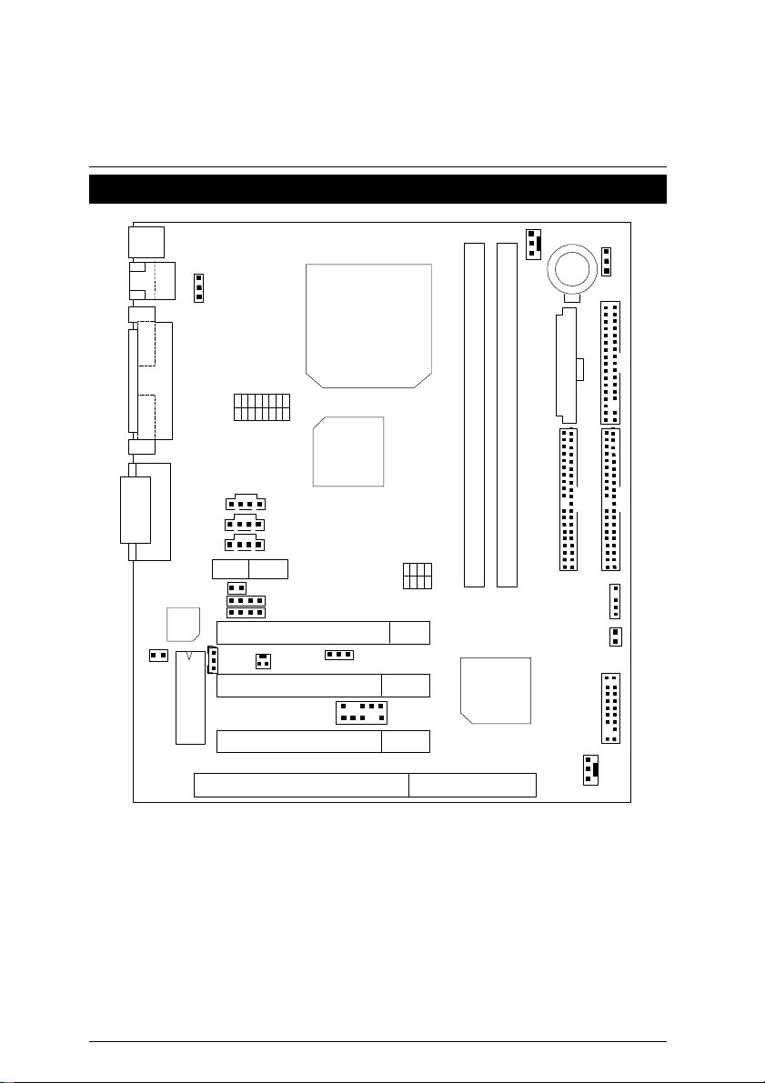
DIMM1
5VMM Motherboard Layout
PS/2
USB
J6
5VMM Motherboard Layout
J1
BAT1
JP2
io
AC97
Socket 7
CPU
SW2
VT8501
J15
J5 J4
Front USB
5VMM
JP4
SW1
VT82C686A
J12
J9
AMR
JP7
JP6
JP5
PCI1
PCI2
PCI3
ISA
J3
JP3
J7
J2
4
Page 12

5VMM Motherboard
$
Page Index for CPU Speed Setup/Connectors/Panel and Jumper Definition
CPU Speed Setup P.6
Connectors P.24
Game & Audio Port P.24
COM A / VGA / LPT Port P.24
USB & LAN Connector P.25
PS/2 Keyboard & PS/2 Mouse Connector P.25
J1 (CPU Fan) P.26
J2 (System Fan) P.26
ATX Power P.27
Front USB [Optional] P.27
Floppy Port P.28
IDE 1(Primary)/ IDE 2(Secondary) Port P.28
J15 (CD Audio Line In) P.29
J12 (AUX_IN)[Optional] P.29
J9 (TEL)[Optional] P.30
J5 (Ring Power On) [Optional] P.30
J4 (Wake on LAN) [Optional] P.31
J3 (IR Connector) P.31
Panel and Jumper Definition P.32
J7 (2x11 Pins Jumper) P.32
JP1 (Clear CMOS Function) P.33
JP5/JP6/JP7 (Onboard AC97& AMR Select) P.33
J6 (USB Device Wake up Selection) [Optional] P.34
JP4 (Onboard LAN Function) [Optional] P.34
JP2 (BIOS Flash ROM Write Protection) [Optional] P.35
JP3 (Internal Buzzer Connector) [Optional] P.35
BAT1 (Battery) P.36
Page
5
Page 13
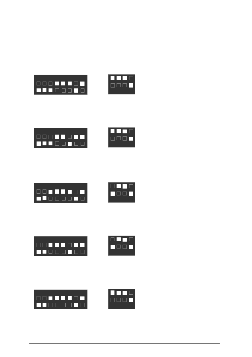
CPU Speed Setup
O: ON/ X: OFF
CPU Speed Setup
The system bus speed is selectable at 66,75,83,90,95,97MHz and 100MHz.
CPU Voltage:
SW2 1 2 3 4 5 SW2 1 2 3 4 5
1.3V X X X X O 2.5V O X O X X
1.4V X O X X O 2.6V X O O X X
1.5V X X O X O 2.7V O O O X X
1.6V X O O X O 2.8V X X X O X
1.7V X X X O O 2.9V O X X O X
1.8V X O X O O 3.0V X O X O X
1.9V X X O O O 3.1V O O X O X
2.0V X O O O O 3.2V X X O O X
2.1V O X X X X 3.3V O X O O X
2.2V X O X X X 3.4V X O O O X
2.3V O O X X X 3.5V O O O O X
2.4V X X O X X --- --- --- --- --- ---
CPU Ratio:
SW2
X1.5
X2 O X X
X2.5
X3 X O X
X3.5
X4 O X O
X4.5
X5 X O O
X5.5
SW1:
FSB
66 O X X X
75 X X X O
83 O X O X
90 O O X X
95 X O O X
97 X X O X
100 O O O X
♦Note: It’s strongly recommended that set the system speed according to your hardware
6 7 8
X X X
O O X
X X X
O O O
X X O
S1 S2 S3 S4
configuration: CPU, SDRAM, Cards, etc
6
Page 14

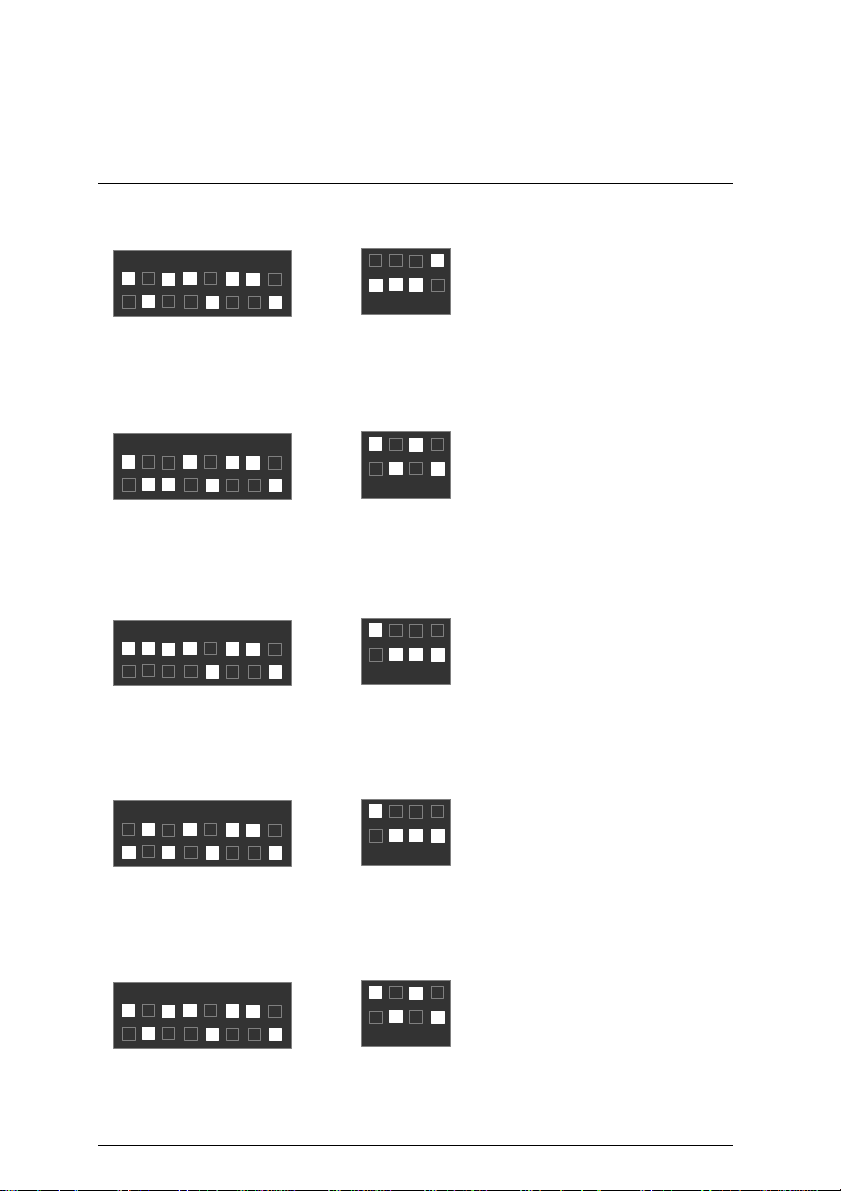
5VMM Motherboard
O: ON / X: OFF
SWITCH
CPU SW
1. Pentium
2. Pentium
3. Pentium
133 MHz O O O O X O X X
166 MHz O O O O X O O X
200 MHz O O O O X X O X
4. Intel MMX-166MHz X X X O X O O X
5. Intel MMX-200MHz X X X O X X O X
6. Intel MMX-233MHz X X X O X X X X
7. AMD-K6/166 (2.9V) O X X O X O O X
8. AMD-K6/200 (2.9V) O X X O X X O X
9. AMD-K6/233 (3.2V) X X O O X X X X
10. AMD-K6/233 (66*3.5 2.2V) X O X X X X X X
11. AMD-K6/266 (66*4 2.2V)
AMD-K6-2/266 (66*4 2.2V)
12. AMD-K6/300 (66*4.5 2.2V) X O X X X O O O
13. AMD-K6/300 (100*3 2.2V)
AMD-K6-2/300 (100*3 2.2V)
14. AMD-K6-2/333 (66*5 2.2V) X O X X X X O O
15.AMD-K6-2/333 (95*3.5 2.2V) X O X X X X X X
16. AMD-K6-2/350 (100*3.5 2.2V) X O X X X X X X
17.AMD-K6-2/366 (66*5.5 2.2V) * X O X X X X X O
18. AMD-K6-2/380 (95*4 2.2V) X O X X X O X O
19. AMD-K6-2/400 (100*4 2.2V) X O X X X O X O
20. AMD-K6-2/450 (100*4.5 2.2V) * X O X X X O O O
21. AMD-K6-2/450 (100*4.5 2.4V) X X O X X O O O
22. AMD-K6-2/475 (95*5 2.2V) * X O X X X X O O
23. AMD-K6-2/475 (95*5 2.4V) * X X O X X X O O
24. AMD-K6-2/500 (100*5 2.2V) *
25.AMD-K6-2/500 (100*5 2.3V) * O O X X X X O O
26. AMD-K6-2/500 (100*5 2.4V) * X X O X X X O O
27. AMD-K6-2/533 (97*5.5 2.2V) *
28. AMD-K6-2/550 (100*5.5 2.2V) *
29. AMD-K6-III/400 (100*4 2.2V) *
30.AMD-K6-III/400 (100*4 2.4V)
S1 S2 S3 S4 S5 S6 S7 S8 S1 S2 S3 S4
X O X X X O X O
X O X X X X O X
X O X
X O X X X X X O
X O X X X X X O
X O X X X O X O
X X O X X O X O
SW 2 SW1
O X X X
O X X X
O X X X
O X X X
O X X X
O X X X
O X X X
O X X X
O X X X
O X X X
O X X X
O X X X
O O O X
O X X X
X O O X
O O O X
O X X X
X O O X
O O O X
O O O X
O O O X
X O O X
X O O X
X X X O O
O O O X
O O O X
O O O X
X X O X
O O O X
O O O X
O O O X
7
Page 15

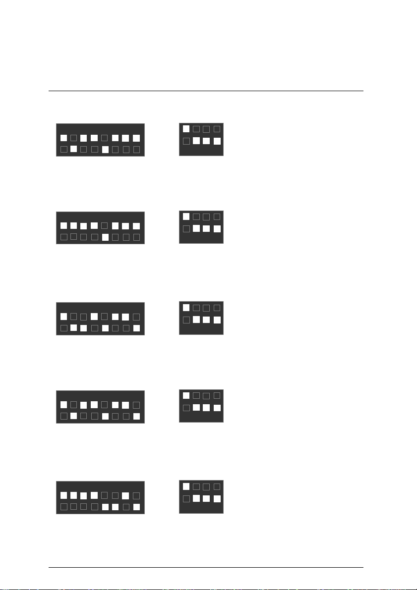
CPU Speed Setup
SWITCH
CPU SW
31.AMD-K6-III/450 (100*4.5 2.2V) *
32.AMD-K6-III/450 (100*4.5 2.4V) *
33.AMD-K6-III/475 (95*5 2.2V) *
34.AMD-K6-III/475 (95*5 2.4V) *
35.AMD-K6-III/500 (100*5 2.2V) *
36.AMD-K6-III/500 (100*5 2.4V) *
37.AMD-K6-III/550 (100*5.5 2.2V) *
38. Cyrix/IBM 6x86MX-PR166
(66*2 2.9V)
39. Cyrix/IBM 6x86MX-PR200
(66*2.5 2.9V)
40. Cyrix/IBM 6x86MX-PR200
(75*2 2.9V)
41. Cyrix/IBM 6x86MX-PR233
(66*3 2.9V)
42. Cyrix/IBM 6x86MX-PR233
(75*2.5 2.9V)
43. Cyrix/IBM 6x86MX-PR233
(83*2 2.9V)
44. Cyrix/IBM 6x86MX-PR266
(66*3.5 2.9V)
45. Cyrix/IBM 6x86MX-PR266
(75*3 2.9V)
46. Cyrix/IBM 6x86MX-PR266
(83*2.5 2.9V)
47. Cyrix M¢º-PR300
(66*3.5 2.9V)
48. Cyrix M¢º-PR333
(66*4 2.9V)
49. Cyrix M¢º-PR333
(83*3 2.9V)
50. Cyrix M¢º-PR333
(75*3.5 2.9V)
51. Cyrix M¢º-PR333
(100*2.5 2.9V)
52. Cyrix M¢º-PR350 *
(90*3 2.9V)
S1 S2 S3 S4 S5 S6 S7 S8 S1 S2 S3 S4
X O X X X O O O
X X O X X O O O
X O X X X X O O
X X O X X X O O
X O X X X X O O
X X O X X X O O
X O X X X X X O
O X X O X O X X
O X X
O X X
O X X
O X X
O X X
O X X
O X X
O X X
O X X
O X X
O X X
O X X
O X X
O X X
SW 2 SW1
O O O X
O O O X
X O O X
X O O X
O O O X
O O O X
O O O X
O X X X
O X O O X
O X O X X
O X X O X
O X O O X
O X O X X
O X X X X
O X X O X
O X O O X
O X X X X
O X O X O
O X X O X
O X X X X
O X O O X
O X X O X
O X X X
X X X O
O X X X
X X X O
O X O X
O X X X
X X X O
O X O X
O X X X
O X X X
O X O X
X X X O
O O O X
O O X X
8
Page 16

5VMM Motherboard
CPU SW
SWITCH
CPU SW
53. Cyrix M¢º-PR366 *
(75*4 2.9V)
54. Cyrix M¢º-PR366 *
(83*3.5 2.9V)
55. Cyrix M¢º-PR366 *
(100*3 2.9V)
56. Cyrix M¢º-PR400 *
(90*4 2.9V)
57. Cyrix M¢º-PR400 *
(100*3.5 2.9V)
58. IDT Winchip 2-200
(66*3 3.5V)
59. IDT Winchip 2-200 *
(100*2 3.5V)
60. IDT Winchip 2-225
(75*3 3.5V)
61. IDT Winchip 2-233 *
(66*3.5 3.5V)
62. IDT Winchip 2-266 *
(66*4 3.5V)
63. IDT Winchip 2-266 *
(100*2.33 3.5V)
64. IDT Winchip 2-300 *
(100*2.5 3.5V)
65. IDT Winchip 3-266 *
(100*2.33 2.8V)
66. RISE MP6-266 *
(100*2 2.8V)
¬Note: If Cyrix 6x86 is being used, please check the CPU Date Code after 605.
MThe default setting is 100*3 at 2.2V for AMD K6/300 and AMD K6-2/300
SWITCH
AMD-K6/300 (100*3 2.2V)
AMD-K6-2/300 (100*3 2.2V)
M The settings of the processors marked with “*” above are just for your reference, these
processors have not been tested yet !
SW 2 SW1
S1 S2 S3 S4 S5 S6 S7 S8 S1 S2 S3 S4
O X X
O X X
O X X
O X X
O X X
O O O O X X O X O X X X
O O O O X O X X O O O X
O O O O X X O X X X X O
O O O O X X X X O X X X
O O O O X O X O O X X X
O O O O X X O O O O O X
O O O O X O O X O O O X
X X X
X X X
S1 S2 S3 S4 S5 S6 S7 S8
X O X X X X O X
O X O X O
O X X X X
O X X O X
O X O X O
O X X X X
O X X O O O O O X
O X O X X O O O X
SW 2 SW1
X X X O
O X O X
O O O X
O O X X
O O O X
S1 S2 S3 S4
O O O X
9
Page 17
1. Pentium Processor 133 MHz
6
5
1
8
3
4
1
6
5
1
8
3
4
1
6
5
1
8
3
4
1
6
5
1
8
3
4
1
CPU Speed Setup
7
4 3
2
ON
SW2
2. Pentium Processor 166 MHz
7
4 3
SW2
2
ON
2
SW1
3. Pentium Processor 200 MHz
7
4 3
SW2
2
ON
2
SW1
4. Intel MMX-166 MHz
ON
2
SW1
ON
ON
7
4 3
SW2
2
ON
2
ON
SW1
10
Page 18
5VMM Motherboard
6
5
1
8
3
4
1
6
5
1
8
3
4
1
6
5
1
8
3
4
1
6
5
1
8
3
4
1
6
5
1
8
3
4
1
5. Intel MMX-200 MHz
7
4 3
2
ON
SW2
6. Intel MMX-233 MHz
7
4 3
2
ON
SW2
7. AMD-K6/166 (2.9V)
7
4 3
2
ON
SW2
8. AMD-K6/200 (2.9V)
7
4 3
2
ON
SW2
9. AMD-K6/233 (3.2V)
ON
2
SW1
ON
2
SW1
ON
2
SW1
ON
2
SW1
7
4 3
SW2
2
ON
2
ON
SW1
11
Page 19

10. AMD-K6/233 (66*3.5 2.2V)
6
5
1
8
3
4
1
6
5
1
8
3
4
1
6
5
1
8
3
4
1
6
5
1
8
3
4
1
6
5
1
8
3
4
1
CPU Speed Setup
7
4 3
SW2
2
ON
2
ON
SW1
11. AMD-K6/266 (66*4 2.2V); AMD-K6-2/266 (66*4 2.2V)
7
4 3
SW2
2
ON
2
ON
SW1
12. AMD-K6/300 (66*4.5 2.2V)
7
4 3
SW2
2
ON
2
ON
SW1
13. AMD-K6/300 (100*3 2.2V); AMD-K6-2/300 (100*3 2.2V)
7
4 3
2
ON
ON
SW2
2
SW1
14. AMD-K6-2/333 (66*5 2.2V)
7
4 3
SW2
2
ON
2
ON
SW1
12
Page 20

5VMM Motherboard
6
5
1
8
3
4
1
6
5
1
8
3
4
1
6
5
1
8
3
4
1
6
5
1
8
3
4
1
6
5
1
8
3
4
1
15. AMD-K6-2/333 (95*3.5 2.2V)
7
4 3
2
ON
SW2
16. AMD-K6-2/350 (100*3.5 2.2V)
7
4 3
2
ON
SW2
17. AMD-K6-2/366 (66*5.5 2.2V)
7
4 3
2
ON
SW2
18. AMD-K6-2/380 (95*4 2.2V)
7
4 3
2
ON
SW2
19. AMD-K6-2/400 (100*4 2.2V)
ON
2
SW1
ON
2
SW1
ON
2
SW1
ON
2
SW1
7
4 3
SW2
2
ON
2
ON
SW1
13
Page 21
20. AMD-K6-2/450 (100*4.5 2.2V)
6
5
1
8
3
4
1
6
5
1
8
3
4
1
6
5
1
8
3
4
1
6
5
1
8
3
4
1
6
5
1
8
3
4
1
CPU Speed Setup
7
4 3
2
ON
SW2
21. AMD-K6-2/450 (100*4.5 2.4V)
7
4 3
2
ON
SW2
22. AMD-K6-2/475 (95*5 2.2V)
7
4 3
2
ON
SW2
23. AMD-K6-2/475 (95*5 2.4V)
7
4 3
2
ON
SW2
24. AMD-K6-2/500 (100*5 2.2V)
ON
2
SW1
ON
2
SW1
ON
2
SW1
ON
2
SW1
7
4 3
SW2
2
ON
2
ON
SW1
14
Page 22

5VMM Motherboard
6
5
1
8
3
4
1
6
5
1
8
3
4
1
6
5
1
8
3
4
1
6
5
1
8
3
4
1
6
5
1
8
3
4
1
25. AMD-K6-2/500 (100*5 2.3V)
7
4 3
2
ON
SW2
26. AMD-K6-2/500 (100*5 2.4V)
7
4 3
2
ON
SW2
27. AMD-K6-2/533 (97*5.5 2.2V)
7
4 3
2
ON
SW2
28. AMD-K6-2/550 (100*5.5 2.2V)
7
4 3
2
ON
SW2
29. AMD-K6-III/400 (100*4 2.2V)
ON
2
SW1
ON
2
SW1
ON
2
SW1
ON
2
SW1
7
4 3
SW2
2
ON
2
ON
SW1
15
Page 23

30. AMD-K6-III/400 (100*4 2.4V)
6
5
1
8
3
4
1
6
5
1
8
3
4
1
6
5
1
8
3
4
1
6
5
1
8
3
4
1
6
5
1
8
3
4
1
CPU Speed Setup
7
4 3
2
ON
SW2
SW1
31. AMD-K6-III/450 (100*4.5 2.2V)
7
4 3
2
ON
SW2
SW1
32. AMD-K6-III/450 (100*4.5 2.4V)
7
4 3
2
ON
SW2
SW1
33. AMD-K6-III/475 (95*5 2.2V)
7
4 3
2
ON
2
ON
2
ON
2
ON
ON
SW2
2
SW1
34. AMD-K6-III/475 (95*5 2.4V)
7
4 3
SW2
2
ON
2
ON
SW1
16
Page 24

5VMM Motherboard
6
5
1
8
3
4
1
6
5
1
8
3
4
1
6
5
1
8
3
4
1
6
5
1
8
3
4
1
6
5
1
8
3
4
1
35. AMD-K6-III/500 (100*5 2.2V)
7
4 3
SW2
2
ON
2
ON
SW1
36. AMD-K6-III/500 (100*5 2.4V)
7
4 3
SW2
2
ON
2
ON
SW1
37. AMD-K6-III/550 (100*5.5 2.2V)
7
4 3
SW2
2
ON
2
ON
SW1
38. Cyrix / IBM 6x86MX-PR166 (66*2 2.9V)
7
4 3
2
ON
ON
SW2
2
SW1
39. Cyrix / IBM 6x86MX-PR200 (66*2.5 2.9V)
7
4 3
SW2
2
ON
2
ON
SW1
17
Page 25

40. Cyrix / IBM 6x86MX-PR200 (75*2 2.9V)
6
5
1
8
3
4
1
6
5
1
8
3
4
1
6
5
1
8
3
4
1
6
5
1
8
3
4
1
6
5
1
8
3
4
1
CPU Speed Setup
7
4 3
SW2
2
ON
2
ON
SW1
41. Cyrix / IBM 6x86MX-PR233 (66*3 2.9V)
7
4 3
SW2
2
ON
2
ON
SW1
42. Cyrix / IBM 6x86MX-PR233 (75*2.5 2.9V)
7
4 3
SW2
2
ON
2
ON
SW1
43. Cyrix / IBM 6x86MX-PR233 (83*2 2.9V)
7
4 3
SW2
2
ON
2
ON
SW1
44. Cyrix / IBM 6x86MX-PR266 (66*3.5 2.9V)
7
4 3
SW2
2
ON
2
ON
SW1
18
Page 26
5VMM Motherboard
6
5
1
8
3
4
1
6
5
1
8
3
4
1
6
5
1
8
3
4
1
6
5
1
8
3
4
1
6
5
1
8
3
4
1
45. Cyrix / IBM 6x86MX-PR266 (75*3 2.9V)
7
4 3
SW2
2
ON
2
ON
SW1
46. Cyrix / IBM 6x86MX-PR266 (83*2.5 2.9V)
7
4 3
SW2
2
ON
2
ON
SW1
47. Cyrix M¢º-PR300 (66*3.5 2.9V)
7
4 3
SW2
2
ON
2
ON
SW1
48. Cyrix M¢º-PR333 (66*4 2.9V)
7
4 3
2
ON
ON
SW2
2
SW1
49. Cyrix M¢º-PR333 (83*3 2.9V)
7
4 3
SW2
2
ON
2
ON
SW1
19
Page 27

50. Cyrix M¢º-PR333 (75*3.5 2.9V)
6
5
1
8
3
4
1
6
5
1
8
3
4
1
6
5
1
8
3
4
1
6
5
1
8
3
4
1
6
5
1
8
3
4
1
CPU Speed Setup
7
4 3
SW2
2
ON
2
SW1
51. Cyrix M¢º-PR333 (100*2.5 2.9V)
7
4 3
SW2
2
ON
2
SW1
52. Cyrix M¢º-PR350 (90*3 2.9V)
7
4 3
SW2
2
ON
2
SW1
53. Cyrix M¢º-PR366 (75*4 2.9V)
7
4 3
2
ON
ON
ON
ON
ON
SW2
2
SW1
54. Cyrix M¢º-PR366 (83*3.5 2.9V)
7
4 3
SW2
2
ON
2
ON
SW1
20
Page 28

5VMM Motherboard
6
5
1
8
3
4
1
6
5
1
8
3
4
1
6
5
1
8
3
4
1
6
5
1
8
3
4
1
6
5
1
8
3
4
1
55. Cyrix M¢º-PR366 (100*3 2.9V)
7
4 3
SW2
2
ON
2
SW1
56. Cyrix M¢º-PR400 (90*4 2.9V)
7
4 3
SW2
2
ON
2
SW1
57. Cyrix M¢º-PR400 (100*3.5 2.9V)
7
4 3
SW2
2
ON
2
SW1
58. IDT Winchip 2-200 (66*3 3.5V)
7
4 3
2
ON
ON
ON
ON
ON
SW2
2
SW1
59. IDT Winchip 2-200 (100*2 3.5V)
7
4 3
SW2
2
ON
2
ON
SW1
21
Page 29

60. IDT Winchip 2-225 (75*3 3.5V)
6
5
1
8
3
4
1
6
5
1
8
3
4
1
6
5
1
8
3
4
1
6
5
1
8
3
4
1
6
5
1
8
3
4
1
CPU Speed Setup
7
4 3
SW2
2
ON
2
SW1
61. IDT Winchip 2-233 (66*3.5 3.5V)
7
4 3
SW2
2
ON
2
SW1
62. IDT Winchip 2-266 (66*4 3.5V)
7
4 3
SW2
2
ON
2
SW1
63. IDT Winchip 2-266 (100*2.33 3.5V)
7
4 3
2
ON
ON
ON
ON
ON
SW2
2
SW1
64. IDT Winchip 2-300 (100*2.5 3.5V)
7
4 3
SW2
2
ON
2
ON
SW1
22
Page 30

5VMM Motherboard
6
5
1
8
3
4
1
6
5
1
8
3
4
1
65. IDT Winchip 3-266 (100*2.33 2.8V)
7
4 3
2
ON
SW2
66. RISE MP6-266 (100*2 2.8V)
7
4 3
SW2
2
ON
ON
2
SW1
ON
2
SW1
23
Page 31

Connectors
Game
Game & Audio Port
Connectors
Port
COM A / VGA / LPT Port
Line Out
COM A
MIC In
Line In
LPT Port
VGA
24
Page 32

5VMM Motherboard
2
1
7
3
USB & LAN Connector (LAN is optional)
1
2
8
5 6
1 – Green LED
(LAN Link LED)
2 – Yellow LED
(LAN Active LED)
PS/2 Keyboard & PS/2 Mouse Connector
PS/2 Mouse
Pin No. Definition
1 USB V0
2 USB D0-
4
3
3 USB D0+
4 GND
5 USB V1
6 USB D17 USB D1+
8 GND
6
4
2
5
1
PS/2 Keyboard
PS/2 Mouse/ Keyboard
Pin No. Definition
1 Data
2 NC
3 GND
4 VCC(+5V)
5 Clock
6 NC
25
Page 33

J1: CPU Fan
J2: System Fan
Connectors
1
Pin No. Definition
1 GND
2 +12V
3 SENSE
1
Pin No. Definition
1 GND
2 +12V
3 SENSE
26
Page 34

5VMM Motherboard
ATX Power
Front USB (Optional)
20
10
11
1
2
1
Pin No. Definition
3,5,7,13,15-17
1,2,11 3.3V
4,6,19,20 VCC
10 +12V
12 -12V
18 -5V
8 Power Good
9 5V SB stand by+5V
14 PS-ON(Soft On/Off)
Pin No. Definition
10
1 5V-SB
2 GND
9
3 USB D24 NC
5 USB D2+
6 USB D37 NC
8 USB D3+
9 GND
10 5V-SB
GND
27
Page 35

Floppy Port
IDE1 (Primary), IDE2 (Secondary) Port
IDE 1 IDE 2
Connectors
Red Line
Red Line
28
Page 36

5VMM Motherboard
J15: CD Audio Line In
J12: AUX_IN (Optional)
1
Pin No. Definition
1 CD-L
2 GND
3 GND
4 CD-R
1
Pin No. Definition
1 AUX-L
2 GND
3 GND
4 AUX-R
29
Page 37

Connectors
J9: TEL: The connector is for Modem with internal voice connector
(Optional)
1
Pin No. Definition
1 Signal -In
2 GND
3 GND
4 Signal-Out
J5: Ring Power On (Internal Modem Card Wake Up) [Optional]
1
Pin No. Definition
1 Signal
2 GND
30
Page 38

5VMM Motherboard
J4: Wake On LAN (Optional)
J3: IR Connector
1
Pin No. Definition
1 +5V SB
2 GND
3 Signal
PIN No. Definition
1
1 VCC (+5V)
2 NC
3 IR data input
4 GND
5 IR data output
31
Page 39

Panel And Jumper Definition
RE
GN
GD
PW
P+ P
S P K
HD
J7: For 2x11 Pins Jumper
Panel and Jumper Definition
1
1
− P−
1
1
1
GN (Green Switch) Open: Normal Operation
Close: Entering Green Mode
GD (Green LED) Pin 1: LED anode(+)
Pin 2: LED cathode(−)
HD (IDE Hard Disk Active LED) Pin 1: LED anode(+)
Pin 2: LED cathode(−)
SPK (Speaker Connector) Pin 1: VCC(+)
Pin 2- Pin 3: NC
Pin 4: Data(−)
RE (Reset Switch) Open: Normal Operation
Close: Reset Hardware System
P+P−P−(Power LED)
Pin 1: LED anode(+)
Pin 2: LED cathode(−)
Pin 3: LED cathode(−)
PW (Soft Power Connector) Open: Normal Operation
Close: Power On/Off
32
Page 40

5VMM Motherboard
JP1: Clear CMOS Function
1
Pin No. Definition
1-2 close Normal (Default)
2-3 close Clear CMOS
JP5/JP6/JP7: Onboard AC97 & AMR (Primary or Secondary) Select
(AMRà Audio Modem Riser)
JP7
JP6
1
Jumper
Function
Only AC97 1-2 Close
Only AMR
(Primary)
AC97+MR
(Secondary)
(Default)
33
3-4 Close
1-2 Close
3-4 Close
JP5
JP5 JP6 JP7
1-2
Close
3-4
Close
1-2
Close
OFF
OFF
ON
Page 41

J6: USB Device Wake up Selection (Optional)
2 close
1
Pin No. Definition
1-2 close Normal (Default)
2-3 close
Enabled USB Device
Wake up
JP4: Onboard LAN Function (Optional)
1
Panel and Jumper Definition
Pin No. Definition
12-3 close Onboard LAN Disabled
Onboard LAN Enabled
(Default)
34
Page 42

5VMM Motherboard
JP2: BIOS Flash ROM Write Protection (Optional)
1
Pin No. Definition
Close BIOS Write Protection
Open Normal (Default)
M
Please set Jumper JP2 to “Open”
to enabled BIOS write function when
you update new BIOS or new device.
JP3: Internal Buzzer Connector (Optional)
1
Pin No.
Definition
Open Internal Buzzer Disabled
Close Internal Buzzer Enabled
(Default)
35
Page 43

BAT1: Battery
+
Danger of explosion if battery
Panel and Jumper Definition
+
is incorrectly replaced.
+ Replace only with the same or
equivalent type recommended
by the manufacturer.
+ Dispose of used batteries
according to the manufacturer’s
instructions.
36
Page 44

5VMM Motherboard
Performance List
The following performance data list is the testing results of some popular benchmark testing
programs.
These data are just referred by users, and there is no responsibility for different testing data
values gotten by users. (The different Hardware & Software configuration will result in different
benchmark testing results.)
• CPU AMD K6-III 450MHz, AMD K6-2 500MHz, AMD K6-2+ 450MHz Processor
• DRAM (128x1) MB SDRAM
• CACHE SIZE 512 KB included in CPU
• DISPLAY Onboard AGP VIA Trident Bland 3D/MVP4 (8MB SDRAM)
• STORAGE Onboard IDE (Quantum KA13600AT)
• O.S. Windows NT
• DRIVER Display Driver at 1024 x 768 x 16bit colors x 75Hz
Winbench99
Business Graphics Winmark 99
Processor
CPU mark99
FPU Winmark 99
Business Disk Winmark 99
Hi-End Graphics Winmark 99
Hi-End Disk Winmark 99
TM
4.0 SPK6
AMD
K6-III 450MHz
(100x4.5)
39.6 12.1 28.8
1520 1570 1520
5090 3350 4620
13300 9910 11500
144 57.4 120
353 122 326
K6-2 500MHz
(100x5)
K6-2+ 450MHz
(100x4.5)
Winstone99
Business Winstone99
Hi-End Winstone99
27.4 14.8 23.7
24.1 13.9 21.5
37
Page 45

USB Bus
48MHz
66 /100 MHz
66 /100 MHz
AMR
Slot
66 /100 MHz
24MHz
Block Diagram
Block Diagram
14.318MHz
Ultra DMA
33/ATA66
IDE Ports
ISA Bus
IDE Bus
AC’97-Link
Socket 7 CPU
VIA
VT8501
PCI Bus
VT82C686A
Host Bus
VIA
33 MHz
33 MHz
14.318MHz
COM Port
3.3V DIMM
DIMM Sockets
ICS 9248-127
LPT
AC97
CODEC
Floppy
PS/2 KB/Mouse
IR
USB Port
38
Page 46

5VMM Motherboard
Memory Installation
The motherboard has 2 dual inline memory module (DIMM) sockets. The BIOS will automatically
detects memory type and size. To install the memory module, just push it vertically into the
DIMM Slot .The DIMM module can only fit in one direction due to the two notch. Memory size
can vary between sockets.
Install memory in any combination table:
DIMM 168-pin SDRAM DIMM Modules
DIMM1 Supports 16 / 32 / 64 / 128 / 256 / 512MB X 1 pcs
DIMM2 Supports 16 / 32 / 64 / 128 / 256 / 512MB X 1 pcs
39
Page 47

BIOS Setup
$ Page Index for BIOS Setup Page
The Main Menu P.42
Standard CMOS Features P.45
Advanced BIOS Features P.49
Advanced Chipset Features P.53
Integrated Peripherals P.56
Power Management Setup P.61
PnP/ PCI Configurations P.65
Frequency / Voltage Control P.67
Load Fail-Safe Defaults P.68
Load Optimized Defaults P.69
Set Supervisor / User Password P.70
Save & Exit Setup P.71
Exit Without Saving P.72
40
Page 48

5VMM Motherboard
BIOS Setup
BIOS Setup is an overview of the BIOS Setup Program. The program that allows users to
modify the basic system configuration. This type of information is stored in battery-backed
CMOS RAM so that it retains the Setup information when the power is turned off.
ENTERING SETUP
Power ON the computer and press <Del> immediately will allow you to enter Setup. If the
message disappears before you respond and you still wish to enter Setup, restart the system to
try again by turning it OFF then ON or pressing the "RESET" bottom on the system case. You
may also restart by simultaneously press <Ctrl> − <Alt>− <Del> keys.
CONTROL KEYS
<↑> Move to previous item
<↓> Move to next item
<←> Move to the item in the left hand
<→> Move to the item in the right hand
<Esc> Main Menu - Quit and not save changes into CMOS
Status Page Setup Menu and Option Page Setup Menu - Exit current page
and return to Main Menu
<+/PgUp> Increase the numeric value or make changes
<-/PgDn> Decrease the numeric value or make changes
<F1> General help, only for Status Page Setup Menu and Option Page Setup
Menu
<F2> Reserved
<F3> Reserved
<F4> Reserved
<F5> Restore the previous CMOS value from CMOS, only for Option Page
Setup Menu
<F6> Load the default CMOS value from BIOS default table, only for Option
Page Setup Menu
<F7>
<F8> Reserved
<F9> Reserved
<F10> Save all the CMOS changes, only for Main Menu
Load the Optimized Defaults
41
Page 49

BIOS Setup
GETTING HELP
Main Menu
The on-line description of the highlighted setup function is displayed at the bottom of the screen.
Status Page Setup Menu / Option Page Setup Menu
Press F1 to pop up a small help window that describes the appropriate keys to use and the
possible selections for the highlighted item. To exit the Help Window press <Esc>.
The Main Menu
Once you enter AMI BIOS CMOS Setup Utility, the Main Menu (Figure 1) will appear on the
screen. The Main Menu allows you to select from nine setup functions and two exit choices. Use
arrow keys to select among the items and press <Enter> to accept or enter the sub-menu.
CMOS Setup Utility-Copyright( C ) 1984-2000 Award Software
Standard CMOS Features Load Fail-Safe Defaults
4
4Advanced BIOS Features Load Optimized Defaults
4Advanced Chipset Features Set Supervisor Password
4Integrated Peripherals Set User Password
4Power Management Setup Save & Exit Setup
4PnP/PCI Configurations Exit Without Saving
4Frequency/Voltage Control
ESC:Quit ↑↓→ ← : Select Item
F10:Save & Exit Setup
Time, Date, Hard Disk Type…
Figure 1: Main Menu
42
Page 50

5VMM Motherboard
•
Standard CMOS Features
This setup page includes all the items in standard compatible BIOS.
•
Advanced BIOS Features
This setup page includes all the items of Award special enhanced features.
•
Advanced Chipset Features
This setup page includes all the items of chipset special features.
•
Integrated Peripherals
This setup page includes all onboard peripherals.
•
Power Management Setup
This setup page includes all the items of Green function features.
•
PnP/PCI Configurations
This setup page includes all the configurations of PCI & PnP ISA resources.
•
Frequency/Voltage Control
This setup page is control CPU’s clock and frequency ratio.
•
Load Fail-Safe Defaults
Fail-Safe Defaults indicates the value of the system parameters which the system would
be in safe configuration.
•
Load Optimized Defaults
Optimized Defaults indicates the value of the system parameters which the system
would be in best performance configuration.
•
Set Supervisor password
Change, set, or disable password. It allows you to limit access to the system and Setup,
or just to Setup.
•
Set User password
Change, set, or disable password. It allows you to limit access to the system.
43
Page 51

•
Save & Exit Setup
Save CMOS value settings to CMOS and exit setup.
•
Exit Without Saving
Abandon all CMOS value changes and exit setup.
BIOS Setup
44
Page 52

5VMM Motherboard
Standard CMOS Features
The items in Standard CMOS Features Menu (Figure 2) are divided into 9 categories. Each
category includes no, one or more than one setup items. Use the arrows to highlight the item
and then use the <PgUp> or <PgDn> keys to select the value you want in each item.
CMOS Setup Utility-Copyright( C ) 1984-2000 Award Software
Date (mm:dd:yy) Fri , Jan 7 2000 Item Help
Time (hh:mm:ss) 2 : 31 : 24
IDE Primary Master Press Enter None
4
4IDE Primary Slave Press Enter None
4IDE Secondary Master Press Enter None
4IDE Secondary Slave Press Enter None
century
Drive A 1.44M, 3.5 in.
Drive B None
Floppy 3 Mode Support Disabled
Video EGA / VGA
Halt On All, But Keyboard
Base Memory 640K
Extended Memory 63488K
Total Memory 64512K
↑↓→ ←:Move Enter:Select +/-/PU/PD:Value F10:Save ESC:Exit F1:General Help
F5:Previous Values F6:Fail-Safe Defaults F7:Optimized Defaults
Standard CMOS Features
Menu Level 4
Change the
Day, month,
Year and
Figure 2: Standard CMOS Features
•
Date
The date format is <week>, <month> <day> <year>.
Week The week, from Sun to Sat, determined by the BIOS and is display-only
Month The month, Jan. Through Dec.
Day The day, from 1 to 31 (or the maximum allowed in the month)
Year The year, from 1994 through 2079
45
Page 53

BIOS Setup
•
Time
The times format in <hour> <minute> <second>. The time is calculated base on the
24-hour military-time clock. For example, 1 p.m. is 13:00:00.
•
IDE Primary Master, Slave / Secondary Master, Slave
The category identifies the types of hard disk from drive C to F that has been installed in
the computer. There are two types: auto type, and user definable type. User type is
user-definable; Auto type which will automatically detect HDD type.
Note that the specifications of your drive must match with the drive table. The hard disk will
not work properly if you enter improper information for this category.
If you select User Type, related information will be asked to enter to the following items.
Enter the information directly from the keyboard and press <Enter>. Such information
should be provided in the documentation form your hard disk vendor or the system
manufacturer.
CYLS. Number of cylinders
HEADS number of heads
PRECOMP write precomp
LANDZONE Landing zone
SECTORS number of sectors
If a hard disk has not been installed select NONE and press <Enter>.
•
Drive A / Drive B
The category identifies the types of floppy disk drive A or drive B that has been installed in
the computer.
None No floppy drive installed.
360K, 5.25 in. 5.25 inch PC-type standard drive; 360K byte capacity.
1.2M, 5.25 in. 5.25 inch AT-type high-density drive; 1.2M byte capacity (3.5 inch
when 3 Mode is Enabled).
720K, 3.5 in. 3.5 inch double-sided drive; 720K byte capacity
1.44M, 3.5 in. 3.5 inch double-sided drive; 1.44M byte capacity.
2.88M, 3.5 in. 3.5 inch double-sided drive; 2.88M byte capacity.
46
Page 54

5VMM Motherboard
•
Floppy 3 Mode Support (for Japan Area)
Disabled Normal Floppy Drive. (Default value)
Drive A Drive A is 3 mode Floppy Drive.
Drive B Drive B is 3 mode Floppy Drive.
Both Drive A & B are 3 mode Floppy Drives.
•
Video
The category detects the type of adapter used for the primary system monitor that must
match your video display card and monitor. Although secondary monitors are supported,
you do not have to select the type in setup.
EGA/VGA Enhanced Graphics Adapter/Video Graphics Array. For EGA, VGA,
SVGA, or PGA monitor adapters.
CGA 40 Color Graphics Adapter, power up in 40 column mode.
CGA 80 Color Graphics Adapter, power up in 80 column mode.
MONO Monochrome adapter, includes high resolution monochrome adapters.
•
Halt on
The category determines whether the computer will stop if an error is detected during
power up.
NO Errors The system boot will not stop for any error that may be
detected and you will be prompted
All Errors Whenever the BIOS detects a non-fatal error the system will
be stopped
All, But Keyboard The system boot will not stop for a keyboard error; it will stop
for all other errors
All, But Diskette The system boot will not stop for a disk error; it will stop for all
other errors
All, But Disk/Key The system boot will not stop for a keyboard or disk error; it
will stop for all other errors
47
Page 55

BIOS Setup
•
Memory
The category is display-only which is determined by POST (Power On Self Test) of the
BIOS.
Base Memory
The POST of the BIOS will determine the amount of base (or conventional)
memory installed in the system.
The value of the base memory is typically 512 K for systems with 512 K
memory installed on the motherboard, or 640 K for systems with 640 K or more
memory installed on the motherboard.
Extended Memory
The BIOS determines how much extended memory is present during the POST.
This is the amount of memory located above 1 MB in the CPU's memory
address map.
48
Page 56

5VMM Motherboard
Advanced BIOS Features
CMOS Setup Utility-Copyright( C ) 1984-2000 Award Software
Advanced BIOS Features
Virus Warning Disabled Item Help
CPU Internal Cache Enabled
Quick Power On Self Test Enabled
First Boot Device Floppy
Second Boot Device HDD-0
Third Boot Device LS120
Boot Other Device Enabled
Swap Floppy Drive Disabled
Boot Up Floppy Seek Enabled
Boot Up NumLock Status On
Gate A20 Option Fast
Typematic Rate Setting Disabled
X Typematic Rate (Chars/Sec) 6
X Typematic Delay (Msec) 250
Security Option Setup
OS Select For DRAM >64MB Non-OS2
HDD S.M.A.R.T. Capability Disabled
Report No FDD For WIN 95 Yes
Video BIOS Shadow Enabled
Menu Level 4
Allows you to
choose the VIRUS
Warning feature
For IDE Hard disk
Boot sector
Protection. If this
Function is enable
And someone
Attempt to write
Data into this area
, BIOS will show
A warning
Message on
Screen and alarm
beep
Cyrix 6x86/M II CPUID Enabled
↑↓→ ←:Move Enter:Select +/-/PU/PD:Value F10:Save ESC:Exit F1:General Help
F5:Previous Values F6:Fail-Safe Defaults F7:Optimized Defaults
Figure 3: Advanced BIOS Features
•
Virus Warning
If it is set to enable, the category will flash on the screen when there is any attempt to write
to the boot sector or partition table of the hard disk drive. The system will halt and the
following error message will appear in the mean time. You can run anti-virus program to
locate the problem.
Enabled Activate automatically when the system boots up causing a warning
message to appear when anything attempts to access the boot sector or
hard disk partition table.
Disabled No warning message to appear when anything attempts to access the
boot sector or hard disk partition table. (Default value)
49
Page 57

BIOS Setup
•
CPU Internal Cache
These two categories speed up memory access. However, it depends on CPU / chipset
design.
Enabled Enabled cache. (Default value)
Disabled Disabled cache.
•
Quick Power On Self Test
This category speeds up Power On Self Test (POST) after you power on the computer. If it
is set to Enable, BIOS will shorten or skip some check items during POST.
Enabled Enabled quick POST. (Default value)
Disabled Normal POST.
First / Second / Third Boot device
•
Floppy Select your boot device priority by Floppy.
LS120 Select your boot device priority by LS120.
HDD-0~3 Select your boot device priority by HDD-0~3.
SCSI Select your boot device priority by SCSI.
CDROM Select your boot device priority by CDROM.
ZIP100 Select your boot device priority by ZIP100.
Disabled Disabled this function.
LAN Select your boot device priority by LAN.
•
Boot other device
Enabled Enabled select your boot device priority function. (Default value)
Disabled Disabled this function.
•
Swap Floppy Drive
Enabled Floppy A & B will be swapped under DOS.
Disabled Floppy A & B will be normal definition. (Default value)
50
Page 58

5VMM Motherboard
•
Boot Up Floppy Seek
During POST, BIOS will determine the floppy disk drive installed is 40 or 80 tracks. 360 K
type is 40 tracks 720 K, 1.2 M and 1.44 M are all 80 tracks.
Enabled BIOS searches for floppy disk drive to determine it is 40 or 80 tracks.
Note that BIOS can not tell from 720 K, 1.2 M or 1.44 M drive type as
they are all 80 tracks. (Default value)
Disabled BIOS will not search for the type of floppy disk drive by track number.
Note that there will not be any warning message if the drive installed is
360 K.
Boot Up NumLock Status
•
On Keypad is number keys. (Default value)
Off Keypad is arrow keys.
Gate A20 Option
•
Normal Set Gate A20 Option is Normal.
Fast Set Gate A20 Option is Fast. (Default value)
•
Typematic Rate Setting
Enabled Enable Keyboard Typematic rate setting.
Disabled Disable Keyboard Typematic rate setting. (Default value)
•
Typematic Rate (Chars / Sec.)
6-30 Set the maximum Typematic rate from 6 chars. Per second to 30
characters. Per second. (Default value: 6)
•
Typematic Delay (Msec.)
250-1000 Set the time delay from first key to repeat the same key in to
computer. (Default value: 250)
•
Security Option
This category allows you to limit access to the system and Setup, or just to Setup.
System The system can not boot and can not access to Setup page will be
denied if the correct password is not entered at the prompt.
Setup The system will boot, but access to Setup will be denied if the correct
password is not entered at the prompt. (Default value)
51
Page 59

BIOS Setup
•
OS Select For DRAM>64MB
Non-OS2 Using non-OS2 operating system. (Default value)
OS2 Using OS2 operating system and DRAM>64MB.
HDD S.M.A.R.T. Capability
•
Enabled Enabled HDD S.M.A.R.T. Capability.
Disabled Disabled HDD S.M.A.R.T. Capability. (Default value)
•
Report No FDD For WIN 95
No Assign IRQ6 For FDD.
Yes FDD Detect IRQ6 Automatically. (Default value)
•
Video BIOS Shadow
It determines whether video BIOS is able to copy to RAM, however, it is optional from
chipset design. Video Shadow will increase the video speed.
Enabled Video shadow is enabled. (Default value)
Disabled Video shadow is disabled.
Cyrix 6x86/M II CPUID
•
Enabled Enabled Cyrix 6x86/M II CPUID. (Default value)
Disabled Disabled this function.
52
Page 60

5VMM Motherboard
Advanced Chipset Features
CMOS Setup Utility-Copyright( C ) 1984-2000 Award Software
Bank 0/1 DRAM Timing SDRAM 10ns Item Help
Bank 2/3 DRAM Timing SDRAM 10ns
SDRAM Cycle Length 3
DRAM Read Pipeline Disabled
Video BIOS Cacheable Enabled
System BIOS Cacheable Enabled
Memory Hole Disabled
Init Display First PCI Slot
Frame Buffer Size 8M
AGP Aperture Size 64M
OnChip USB Enabled
USB Keyboard Support Disabled
OnChip Sound Enabled
OnChip Modem Enabled
Memory Parity/ECC Check Disabled
↑↓→ ←:Move Enter:Select +/-/PU/PD:Value F10:Save ESC:Exit F1:General Help
F5:Previous Values F6:Fail-Safe Defaults F7:Optimized Defaults
Advanced Chipset Features
Menu Level 4
Figure 4: Advanced Chipset Features
•
Bank 0/1, 2/3 DRAM Timing
SDRAM 10ns For SDRAM 10ns DRAM timing operation. (Default Value)
SDRAM 8ns For SDRAM 8ns DRAM timing operation.
Normal For Normal DRAM timing operation.
Medium For Medium DRAM timing operation.
Fast For Fast DRAM timing operation.
Turbo For Turbo DRAM timing operation.
SDRAM Cycle Length
•
3 Set SDRAM Cycle Length to 3. (Default Value)
2 Set SDRAM Cycle Length to 2.
•
DRAM Read Pipeline
Enabled Enabled DRAM Read Pipeline.
Disabled Disabled DRAM Read Pipeline. (Default value)
53
Page 61

•
Video BIOS Cacheable
Enabled Enabled video BIOS Cacheable. (Default value)
Disabled Disabled video BIOS Cacheable.
•
System BIOS Cacheable
Enabled Enable System BIOS Cacheable. (Default value)
Disabled Disable System BIOS Cacheable.
•
Memory Hole
Disabled Normal Setting. (Default value)
15M-16M Set Address=15~16MB remap to ISA BUS.
Init Display First
•
PCI Slot System will boot from PCI VGA Card first. (Default value)
AGP System will boot from AGP Display Card first.
•
Frame Buffer Size
4MB Set Frame Buffer Size to 4MB.
8MB Set Frame Buffer Size to 8 MB. (Default Value)
NA Disabled this function.
•
AGP Aperture Size
BIOS Setup
4MB Set AGP Aperture Size to 4MB.
8MB Set AGP Aperture Size to 8MB.
16MB Set AGP Aperture Size to 16MB.
32MB Set AGP Aperture Size to 32MB.
64MB Set AGP Aperture Size to 64MB. (Default Value)
128MB Set AGP Aperture Size to 128MB.
•
OnChip USB
Enabled Enabled OnChip USB. (Default value)
Disabled Disabled USB Controller.
•
USB Keyboard Support
Enabled Enabled USB Keyboard Support.
Disabled Disabled USB Keyboard Support. (Default value)
54
Page 62

5VMM Motherboard
•
OnChip Sound
Enabled Enabled OnChip Sound. (Default Value)
Disabled Disabled this function.
•
OnChip Modem
Enabled Enabled OnChip Modem. (Default Value)
Disabled Disabled this function.
Memory Parity/ECC Check
•
Enabled Enabled Memory Parity/ECC Check Function.
Disabled Disabled Memory Parity/ECC Check Function. (Default Value)
55
Page 63

Integrated Peripherals
BIOS Setup
CMOS Setup Utility-Copyright( C ) 1984-1999 Award Software
Integrated Peripherals
OnChip IDE Channel 0 Enabled Item Help
OnChip IDE Channel 1 Enabled
IDE Prefetch Mode Enabled
Primary Master PIO Auto
Primary Slave PIO Auto
Secondary Master PIO Auto
Secondary Slave PIO Auto
Primary Master UDMA Auto
Primary Slave UDMA Auto
Secondary Master UDMA Auto
Secondary Slave UDMA Auto
IDE HDD Block Mode Enabled
Onboard FDD Controller Enabled
Onboard Serial Port 1 Auto
Onboard Serial Port 2 Auto
UART 2 Mode HPSIR
IR Function Duplex Half
TX, RX inverting enable No, Yes
Onboard Parallel Port 378/IRQ7
Onboard Parallel Mode Normal
ä
ECP Mode Use DMA 3
ä Parallel Port EPP Type EPP1.9
Onboard Legacy Audio Enabled
Sound Blaster Disabled
SB I/O Base Address 220H
SB IRQ Select IRQ5
SB DMA Select DMA1
MPU-401 Disabled
MPU-401 I/O Address 330-333H
Game Port (200-207H) Enabled
↑↓→ ←:Move Enter:Select +/-/PU/PD:Value F10:Save ESC:Exit F1:General Help
F5:Previous Values F6:Fail-Safe Defaults F7:Optimized Defaults
Menu Level 4
Figure 5: Integrated Peripherals
ä These two items will be available when ”Onboard Parallel Mode” is set to ECP+EPP.
•
OnChip IDE Channel 0
Enabled Enabled onboard 1st channel IDE port. (Default value)
Disabled Disabled onboard 1st channel IDE port.
56
Page 64

5VMM Motherboard
•
OnChip IDE Channel 1
Enabled Enabled onboard 2nd channel IDE port. (Default value)
Disabled Disabled onboard 2nd channel IDE port.
•
IDE Prefetch Mode
Enabled Enabled IDE Prefetch Mode. (Default value)
Disabled Disabled IDE Prefetch Mode.
•
Primary Master PIO (for onboard IDE 1st channel)
Auto BIOS will automatically detect the IDE HDD Accessing mode.
(Default value)
Mode0~4 Manually set the IDE Accessing mode.
•
Primary Slave PIO (for onboard IDE 1st channel)
Auto BIOS will automatically detect the IDE HDD Accessing mode.
(Default value)
Mode0~4 Manually set the IDE Accessing mode.
•
Secondary Master PIO (for onboard IDE 2nd channel)
Auto BIOS will automatically detect the IDE HDD Accessing mode.
(Default value)
Mode0~4 Manually set the IDE Accessing mode.
•
Secondary Slave PIO (for onboard IDE 2nd channel)
Auto BIOS will automatically detect the IDE HDD Accessing mode.
(Default value)
Mode0~4 Manually set the IDE Accessing mode.
•
Primary Master UDMA
Auto BIOS will automatically detect the IDE HDD Accessing mode.
(Default value)
Disabled Disable UDMA function.
•
Primary Slave UDMA
Auto BIOS will automatically detect the IDE HDD Accessing mode.
(Default value)
Disabled Disable UDMA function.
57
Page 65

•
Secondary Master UDMA
Auto BIOS will automatically detect the IDE HDD Accessing mode.
(Default value)
Disabled Disable UDMA function.
•
Secondary Slave UDMA
Auto BIOS will automatically detect the IDE HDD Accessing mode.
(Default value)
Disabled Disable UDMA function.
•
IDE HDD Block Mode
Enabled Enabled IDE HDD Block Mode. (Default value)
Disabled Disabled IDE HDD Block Mode.
•
Onboard FDD Controller
Enabled Enabled onboard FDD port. (Default value)
Disabled Disabled onboard FDD port.
•
Onboard Serial Port 1
Auto BIOS will automatically setup the port 1 address. (Default value)
3F8/IRQ4 Enable onboard Serial port 1 and address is 3F8.
2F8/IRQ3 Enable onboard Serial port 1 and address is 2F8.
3E8/IRQ4 Enable onboard Serial port 1 and address is 3E8.
2E8/IRQ3 Enable onboard Serial port 1 and address is 2E8.
Disabled Disable onboard Serial port 1.
BIOS Setup
•
Onboard Serial Port 2
Auto BIOS will automatically setup the port 2 address. (Default value)
3F8/IRQ4 Enable onboard Serial port 2 and address is 3F8.
2F8/IRQ3 Enable onboard Serial port 2 and address is 2F8.
3E8/IRQ4 Enable onboard Serial port 2 and address is 3E8.
2E8/IRQ3 Enable onboard Serial port 2 and address is 2E8.
Disabled Disable onboard Serial port 2.
58
Page 66

5VMM Motherboard
• UART 2 Mode
(This item allows you to determine which UART 2 Mode of onboard I/O chip)
HPSIR Set onboard I/O chip UART 2 to HPSIR mode. (Default Value)
ASKIR Set onboard I/O chip UART 2 to ASKIR Mode.
• IR Function Duplex
Half
Full
IR Function Duplex Half. (Default Value)
IR Function Duplex Full.
• TX, RX Inverting enabled
No, Yes
Yes, No
No, No
Yes, Yes
•
Onboard Parallel port
378/IRQ7 Enabled onboard LPT port and address is 378/IRQ7. (Default value)
278/IRQ5 Enabled onboard LPT port and address is 278/IRQ5.
Disabled Disabled onboard LPT port.
3BC/IRQ7 Enabled onboard LPT port and address is 3BC/IRQ7.
•
Onboard Parallel Mode
Normal Normal Setting. (Default value)
EPP Using Parallel port as Enhanced Parallel Port.
ECP Using Parallel port as Extended Capabilities Port.
ECP+EPP Using Parallel port as ECP & EPP mode.
•
ECP Mode Use DMA
1 Set ECP Mode Use DMA is 1.
3 Set ECP Mode Use DMA is 3. (Default value)
Set TX, RX Inverting enabled to No, Yes. (Default Value)
Set TX, RX Inverting enabled to Yes, No.
Set TX, RX Inverting enabled to No, No.
Set TX, RX Inverting enabled to Yes, Yes.
•
Parallel Port EPP Type
EPP 1.9 EPP Version is 1.9. (Default value)
EPP 1.7 EPP Version is 1.7.
59
Page 67

•
Onboard Legacy Audio
Enabled Enabled Onboard Legacy Audio. (Default Value)
Disabled Disabled Onboard Legacy Audio.
•
Sound Blaster
Enabled Enabled Sound Blaster.
Disabled Disabled Sound Blaster. (Default Value)
•
SB I/O Base Address
220H Set SB I/O Base Address is 220h. (Default Value)
240H Set SB I/O Base Address is 240h.
260H Set SB I/O Base Address is 260h.
280H Set SB I/O Base Address is 280h.
•
SB IRQ Select
IRQ 5 / 9 / 10. (Default Value: 5 )
•
SB DMA Select
DMA 0 / 1 / 2/ 3. (Default Value: 1 )
•
MPU-401
BIOS Setup
Enabled Enabled MPU-401.
Disabled Disabled MPU-401. (Default Value)
•
MUP-401 I/O Address
330-333H Set MUP-401 I/O Address is 330-333H. (Default Value)
300-303H Set MUP-401 I/O Address is 300-303H.
310-313H Set MUP-401 I/O Address is 310-313H.
320-323H Set MUP-401 I/O Address is 320-323H.
•
Game Port (200-207H)
Disabled Disabled Game Port (200-207H).
Enabled Enabled Game Port (200-207H). (Default Value)
60
Page 68

5VMM Motherboard
Power Management Setup
CMOS Setup Utility-Copyright( C ) 1984-2000 Award Software
„Power Management Press Enter Item Help
PM Control by APM Yes
Video Off Option SuspendgOff
Video Off Method DPMS Support
MODEM Use IRQ 4
Soft-Off by PWRBTN Instant-Off
AC Back Function Memory
CPU Fan In Suspend Off
„Wake Up Events Press Enter
↑↓→ ←:Move Enter:Select +/-/PU/PD:Value F10:Save ESC:Exit F1:General Help
F5:Previous Values F6:Fail-Safe Defaults F7:Optimized Defaults
Power Management Setup
Menu Level 4
Figure 6: Power Management Setup
•
Power Management
User Define For configuring our own power management features. (Default value)
Min Saving Minimum power saving.
Max Saving Maximum power saving.
•
HDD Power Down
Disabled Disabled HDD Power Down mode function. (Default value)
1-15 mins Enabled HDD Power Down mode between 1 to 15 mins.
•
Doze Mode
Disabled Disabled Doze Mode.
10Sec - 1 Hour Setup the timer to enter Doze Mode.
•
Suspend Mode
Disabled Disabled Suspend Mode.
10Sec - 1 Hour Setup the timer to enter Suspend Mode.
61
Page 69

•
PM Control by APM
Yes Enabled PM Control by APM. (Default value)
No Disabled this function.
•
Video off Option
SuspendgOff BIOS will turn off V/H-SYNC when gets into Green mode for
Green monitor power saving. (Default value)
All ModesgOff BIOS will turn off V/H-SYNC when all modes.
Always On BIOS will turn always on when all modes.
•
Video off Method
V/H SYNC+Blank BIOS will turn off V/H-SYNC when gets into Green mode for
Green monitor power saving.
Blank Screen BIOS will only black monitor when gets into Green mode.
DPMS Support BIOS will use DPMS Standard to control VGA card. (The Green
type VGA card will turn off V/H-SYNC automatically.)
(Default value)
•
MODEM Use IRQ
NA Set MODEM Use IRQ to NA.
3 Set MODEM Use IRQ to 3.
4 Set MODEM Use IRQ to 4. (Default value)
5 Set MODEM Use IRQ to 5.
7 Set MODEM Use IRQ to 7.
9 Set MODEM Use IRQ to 9.
10 Set MODEM Use IRQ to 10.
11 Set MODEM Use IRQ to 11.
BIOS Setup
•
Soft-off by PWR-BTTN
Instant-off Soft switch ON/OFF for POWER ON/OFF. (Default value)
Delay 4 Sec. Soft switch ON 4sec. for POWER OFF.
•
AC Back Function
Memory This function depends on computer status. (Default value)
Soft-Off Set System Soft-Off Status.
Full-On Set System Full-On Status.
62
Page 70

5VMM Motherboard
•
CPU Fan In Suspend
Off Disabled this function. (Default value)
On Stop CPU FAN when entering Suspend mode.
•
VGA
OFF
ON
•
LPT & COM
LPT/COM Enabled LPT/COM Ports Activity. (Default value)
NONE Normal Operation.
LPT Enabled LPT Ports Activity.
COM Enabled COM Ports Activity.
•
HDD & FDD
ON Enabled HDD & FDD Ports Activity. (Default value)
OFF Disabled HDD & FDD Ports Activity.
•
DMA/master
ON Don’t detect DMA/master PM event.
OFF Normal Operation. (Default value)
•
PowerOn by PCI Card
Disabled Disabled this function.
Enabled Enabled PowerOn by PCI Card. (Default value)
•
Wake Up On LAN/Ring
Disabled Disabled this function.
Enabled Enabled Wake Up On LAN/Ring. (Default value)
Disabled monitor VGA activity. (Default value)
Enabled monitor VGA activity.
63
Page 71

•
RTC Alarm Resume
You can set “RTC Alarm Resume” item to Enabled and key in date/time to power on
system.
Disabled Disabled this function. (Default value)
Enabled Enabled alarm function to POWER ON system.
If the “RTC Alarm Resume” is Enabled.
Date ( of Month) Alarm : 0~31
Resume Time ( hh: mm: ss) Alarm : (0~23) : (0~59) : (0~59)
•
Primary INTR
OFF Disabled this function.
ON Enabled Primary INTR Function. (Default value)
•
IRQ [3-15]
Disabled Disabled this function.
Primary The resource is used by Primary device.
Secondary The resource is used by Secondary device.
BIOS Setup
64
Page 72

5VMM Motherboard
PnP/PCI Configurations
CMOS Setup Utility-Copyright( C ) 1984-2000 Award Software
PnP/PCI Configurations
PNP OS Installed No Item Help
Reset Configuration Data Disabled
Resources Controlled By Auto (ESCD)
X IRQ Resources Press Enter
X DMA Resources Press Enter
PCI/VGA Palette Snoop Disabled
Assign IRQ For VGA Enabled
Assign IRQ For USB Enabled
Menu Level 4
When resources are
controlled manually,
assign each system
interrupt a type,
depending on the type
of device using the
Interrupt.
↑↓→ ←Move Enter:Select +/-/PU/PD:Value F10:Save ESC:Exit F1:General Help
F5:Previous Values F6:Fail-Safe Defaults F7:Optimized Defaults
Figure 7: PnP/PCI Configurations
•
PNP OS Installed
Yes Enable PNP OS Installed function.
No Disable PNP OS Installed function. (Default value)
•
Reset Configuration Data
Disabled Disabled this function. (Default value)
ESCD Clear PnP information in ESCD.
DMI Update Desktop Management Information data.
Both Clear PnP information in ESCD & update DMI data.
65
Page 73

•
Resources Controlled by
Manual User can set the PnP resource (I/O Address, IRQ & DMA channels)
used by legacy ISA DEVICE.
Auto(ESCD) BIOS automatically use these PnP rescuers. (Default value)
•
IRQ ( 3,4,5,7,9, 10,11,12,14,15 ),DMA( 0,1,3,5,6,7 )
Legacy ISA The resource is used by Legacy ISA device.
PCI/ISA PnP The resource is used by PCI/ISA PnP device (PCI or ISA).
•
PCI/VGA Palette Snoop
Enabled For having Video Card on ISA Bus and VGA Card on PCI Bus.
Disabled For VGA Card only. (Default value)
•
Assign IRQ For VGA
Enabled Assign a specific IRQ for VGA. (Default value)
Disabled No IRQ is assigned for VGA.
•
Assign IRQ For USB
Enabled Assign a specific IRQ for USB. (Default value)
Disabled No IRQ is assigned for USB.
BIOS Setup
66
Page 74

5VMM Motherboard
Frequency/Voltage Control
CMOS Setup Utility-Copyright( C ) 1984-2000 Award Software
Auto Detect DIMM/PCI Clk Enabled Item Help
Spread Spectrum Modulated Disabled
↑↓→ ←Move Enter:Select +/-/PU/PD:Value F10:Save ESC:Exit F1:General Help
F5:Previous Values F6:Fail-Safe Defaults F7:Optimized Defaults
Frequency/Voltage Control
Menu Level 4
Figure 8: Frequency/Voltage Control
•
Auto Detect DIMM/PCI Clk
Disabled Disabled Auto Detect DIMM/PCI Clk.
Enabled Enabled Auto Detect DIMM/PCI Clk. (Default value)
•
Spread Spectrum Modulated
Disabled Disabled this function. (Default value)
±0.25% Set Spread Spectrum to ±0.25%.
−0.5% Set Spread Spectrum to −0.5%.
67
Page 75

Load Fail-Safe Defaults
BIOS Setup
CMOS Setup Utility-Copyright( C ) 1984-2000 Award Software
Standard CMOS Features Load Fail - Safe Defaults
4
4Advanced BIOS Features Load Optimized Defaults
4Advanced Chipset Features Set Supervisor Password
4Integrated Peripherals Set User Password
4Power Management Setup Save & Exit Setup
4PnP/PCI Configurations Exit Without Saving
4Frequency/Voltage Control
ESC:Quit ↑↓→ ← : Select Item
F10:Save & Exit Setup
•
Load Fail-Safe Defaults
Fail−Safe defaults contain the most appropriate values of the system parameters that allow
minimum system performance.
Load Fail-Safe Defaults (Y/N)? N
Load Fail-Safe Defaults
Figure 9: Load Fail-Safe Defaults
68
Page 76

5VMM Motherboard
Load Optimized Defaults
CMOS Setup Utility-Copyright( C ) 1984-2000 Award Software
Standard CMOS Features Load Fail-Safe Defaults
4
4Advanced BIOS Features Load Optimized Defaults
4Advanced Chipset Features Set Supervisor Password
4Integrated Peripherals Set User Password
4Power Management Setup Save & Exit Setup
4PnP/PCI Configurations Exit Without Saving
4Frequency/Voltage Control
ESC:Quit ↑↓→ ← : Select Item
F10:Save & Exit Setup
•
Load Optimized Defaults
Selecting this field loads the factory defaults for BIOS and Chipset Features which the
system automatically detects.
Load Optimized Defaults (Y/N)? N
Load Optimized Defaults
Figure 10: Load Optimized Defaults
69
Page 77

BIOS Setup
Set Supervisor / User Password
When you select this function, the following message will appear at the center of the screen to
assist you in creating a password.
CMOS Setup Utility-Copyright( C ) 1984-2000 Award Software
Standard CMOS Features Load Fail-Safe Defaults
4
4Advanced BIOS Features Load Optimized Defaults
4Advanced Chipset Features Set Supervisor Password
4Integrated Peripherals Set User Password
4Power Management Setup Save & Exit Setup
PnP/PCI Configurations Exit Without Saving
4
4Frequency/Voltage Control
ESC:Quit ↑↓→ ← : Select Item
F10:Save & Exit Setup
Type the password, up to eight characters, and press <Enter>. The password typed now will
clear the previously entered password from CMOS memory. You will be asked to confirm the
password. Type the password again and press <Enter>. You may also press <Esc> to abort the
selection and not enter a password.
To disable password, just press <Enter> when you are prompted to enter password. A message
“PASSWORD DISABLED” will appear to confirm the password being disabled. Once the
password is disabled, the system will boot and you can enter Setup freely.
If you select “System” at “Security Option” in BIOS Features Setup Menu, you will be prompted
for the password every time the system is rebooted or any time you try to enter Setup Menu. If
you select “Setup” at “Security Option” in BIOS Features Setup Menu, you will be prompted only
when you try to enter Setup.
Enter Password:
Change / Set / Disable Password
Figure 11: Password Setting
70
Page 78

5VMM Motherboard
Save & Exit Setup
CMOS Setup Utility-Copyright( C ) 1984-2000 Award Software
Standard CMOS Features Load Fail-Safe Defaults
4
4Advanced BIOS Features Load Optimized Defaults
4Advanced Chipset Features Set Supervisor Password
4Integrated Peripherals Set User Password
4Power Management Setup Save & Exit Setup
4PnP/PCI Configurations Exit Without Saving
4Frequency/Voltage Control
ESC:Quit ↑↓→ ← : Select Item
F10:Save & Exit Setup
Type "Y" will quit the Setup Utility and save the user setup value to RTC CMOS.
Type "N" will return to Setup Utility.
SAVE to CMOS and EXIT (Y/N)? Y
Save Data to CMOS
Figure 12: Save & Exit Setup
71
Page 79

Exit Without Saving
BIOS Setup
CMOS Setup Utility-Copyright( C ) 1984-2000 Award Software
Standard CMOS Features Load Fail-Safe Defaults
4
4Advanced BIOS Features Load Optimized Defaults
4Advanced Chipset Features Set Supervisor Password
4Integrated Peripherals Set User Password
4Power Management Setup Save & Exit Setup
4PnP/PCI Configurations Exit Without Saving
4Frequency/Voltage Control
ESC:Quit ↑↓→ ← : Select Item
F10:Save & Exit Setup
Quit Without Saving (Y/N)? N
Abandon all Datas
Figure 13: Exit Without Saving
Type "Y" will quit the Setup Utility without saving to RTC CMOS.
Type "N" will return to Setup Utility.
72
Page 80

5VMM Motherboard
1.Click “VIA 4in 1 Service Pack
Appendix
Appendix A: VIA Chipsets Driver
A. VIA 4 in 1 Service Pack Utility:
Insert the support CD that came with your motherboard into your CD-ROM driver or
double –click the CD driver icon in My Computer to bring up the screen.
Chipset
Utility” item.
(1)
3.Click “Yes”
(3)
2.Click “Next”
(2)
4.Click “Next”.
(4)
5.Click “Next”.
(5)
6.Click “Next”.
(6)
73
Page 81

10.Click “Finish” to
Appendix
7.Click “Next”.
(7)
9.Click “Next”.
(9)
8.Click “Next”.
(8)
restart.
(10)
74
Page 82

5VMM Motherboard
5.Click “Next”.
4.You can select “Specify a location:
Win9x then
1.Click “Change” item.
B. VGA Driver:
Insert the support CD that came with your motherboard into your CD-ROM driver or
double –click the CD driver icon in My Computer to bring up the screen.
2. Click “Next”.
(1)
3.Click “Next”.
D:\VIA\VGA\Trident\8400\
Click “Next”.
(2)
(3)
(5)
(4)
6.Click “Next” item.
(6)
75
Page 83

7.Click “Finish” to
Appendix
restart computer.
(7)
76
Page 84

5VMM Motherboard
2.Click “Next”.
Appendix B: VIA Sound Driver
A. AC’97 Audio Driver:
Insert the support CD that came with your motherboard into your CD-ROM driver or
double –click the CD driver icon in My Computer to bring up the screen.
Audio
1.Click “AC’97 Audio Driver” item.
(1)
(2)
3.Click “Next”
(3)
4.Click “Finish” to restart.
(4)
77
Page 85

Appendix
Appendix C: BIOS Flash Procedure
BIOS update procedure:
ü Please check your BIOS vendor (AMI or AWARD) on the motherboard.
ü It is recommended you copy the AWDFlash.exe or AMIFlash.exe in driver CD
(D:\>Utility\BIOSFlash) and the BIOS binary files into the directory you made in your hard
disk. i.e:C:\>Utility\ (C:\>Utility : denotes the driver and the directory where you put the
flash utilities and BIOS file in.)¡j
ü Restart your computer into MS-DOS mode or command prompt only for Win95/98, go into
the directory where the new BIOS file are located use the utility AWDFlash.exe or
AMIFlash.exe to update the BIOS.
ü Type the following command once you have enter the directory where all the files are
located C:\utility\ AWDFlash or AMIFlash <filename of the BIOS binary file intended for
flashing>.
ü Once the process is finished, reboot the system.
MNote: Please download the newest BIOS from our website (www.gigabyte.com.tw) or contact
your local dealer for the file.
78
Page 86

5VMM Motherboard
Appendix D: Acronyms
Acor. Meaning
ACPI Advanced Configuration and Power Interface
POST Power-On Self Test
LAN Local Area Network
ECP Extended Capabilities Port
APM Advanced Power Management
DMA Direct Memory Access
MHz Megahertz
ESCD Extended System Configuration Data
CPU Central Processing Unit
SMP Symmetric Multi-Processing
USB Universal Serial Bus
OS Operating System
ECC Error Checking and Correcting
IDE Integrated Dual Channel Enhanced
SCI Special Circumstance Instructions
LBA Logical Block Addressing
EMC Electromagnetic Compatibility
BIOS Basic Input / Output System
SMI System Management Interrupt
IRQ Interrupt Request
NIC Network Interface Card
A.G.P. Accelerated Graphics Port
S.E.C.C. Single Edge Contact Cartridge
LED Light Emitting Diode
EPP Enhanced Parallel Port
CMOS Complementary Metal Oxide Semiconductor
I/O Input / Output
ESD Electrostatic Discharge
OEM Original Equipment Manufacturer
SRAM Static Random Access Memory
VID Voltage ID
DMI Desktop Management Interface
MIDI Musical Interface Digital Interface
IOAPIC Input Output Advanced Programmable Input Controller
DIMM Dual Inline Memory Module
DRAM Dynamic Random Access Memory
PAC PCI A.G.P. Controller
AMR Audio Modem Riser
To be continued…
79
Page 87

Acor. Meaning
PCI Peripheral Component Interconnect
RIMM Rambus in-line Memory Module
DRM Dual Retention Mechanism
ISA Industry Standard Architecture
MTH Memory Translator Hub
CRIMM Continuity RIMM
Appendix
80
 Loading...