

Page 1

5SMM
TABLE OF CONTENTS
1. INTRODUCTION
1.1. PREFACE................................................................................. 1-1
1.2. KEY FEATURES....................................................................... 1-1
1.3. PERFORMANCE LIST .............................................................. 1-3
1.4. BLOCK DIAGRAM..................................................................... 1-4
1.5. INTRODUCE THE PCI - BUS.................................................... 1-5
1.6. FEATURES...............................................................................1-5
2. SPECIFICATION
2.1. HARDWARE............................................................................. 2-1
2.2. SOFTWARE.............................................................................. 2-2
2.3. ENVIRONMENT........................................................................2-2
3. HARDWARE INSTALLATION
3.1. UNPACKING............................................................................. 3-1
3.2. MAINBOARD LAYOUT .............................................................. 3-2
3.3. QUICK REFERENCE FOR JUMPERS & CONNECTORS.......... 3-2
3.4. SRAM INSTALLATION DRAM INSTALLATION.......................... 3-6
3.5. DRAM INSTALLATION .............................................................. 3-6
3.6. CPU INSTALLATION AND JUMPERS SETUP ........................... 3-7
3.7. CMOS RTC & ISA CFG CMOS SRAM ....................................... 3-8
3.8. SPEAKER CONNECTOR INSTALLATION................................. 3-9
3.9. HARDWARE RESET SWITCH CONNECTOR INSTALLATION... 3-9
1
Page 2

3.10. GREEN FUNCTION INSTALLATION....................................... 3-9
3.11. PERIPHERAL DEVICE INSTALLATION................................... 3-9
4. BIOS CONFIGURATION
4.1. ENTERING SETUP................................................................... 4-1
4.2. CONTROL KEYS ...................................................................... 4-2
4.3. GETTING HELP........................................................................ 4-3
4.3.1.Main Menu ....................................................................... 4-3
4.3.2.Status Page Setup Menu / Option Page Setup Menu.......... 4-3
4.4. THE MAIN MENU...................................................................... 4-3
4.5. STANDARD CMOS SETUP MENU............................................ 4-5
4.6. BIOS FEATURES SETUP ......................................................... 4-9
4.7. CHIPSET FEATURES SETUP................................................... 4-13
4.8. POWER MANAGEMENT SETUP.............................................. 4-18
4.9. PNP/PCI CONFIGURATION...................................................... 4-21
Table Of Contents
4.10. LOAD BIOS DEFAULTS.......................................................... 4-23
4.11. LOAD SETUP DEFAULTS ....................................................... 4-24
4.12. INTEGRATED PERIPHERALS ................................................ 4-25
4.13. PASSWORD SETTING........................................................... 4-31
4.14. IDE HDD AUTO DETECTION.................................................. 4-32
4.15. SAVE & EXIT SETUP.............................................................. 4-33
4.16. EXIT WITHOUT SAVING ........................................................ 4-34
APPENDIX A: Onboard Driver Installation Procedure ................. A-1
2
Page 3

5SMM
1. INTRODUCTION
1.1. PREFACE
Welcome to use the 5SMM motherboard. The motherboard is a Pipeline 512 KB
CACHE Pentium Processor based PC / AT compatible system with ISA bus and
PCI Local Bus, and has been designed to be the fastest PC / AT system. There are
some new features allow you to operate the system with the performance you want.
This manual also explains how to install the motherboard for operation, and how to
set up your CMOS CONFIGURATION with BIOS SETUP program.
1.2. KEY FEATURES
q Pentium
q 3 PCI Bus slots, 2 ISA Bus slots.
q Supports :
• Pentium
• AMD
Processor based PC / AT compatible mainboard with PCI / ISA / BUS.
Processor
:133/166/200 MHz; MMX (166 / 200 / 233)
:K6-(166 / 200 / 233 / 266 / 300)
K6-2(266 / 300 / 333 / 350 / 366 / 380 / 400 / 450 /
475 / 500 / 550)
K6-III(400 / 450 / 475 / 500 / 550)
• Cyrix/IBM
:6x86MX (PR166 / PR200 / PR233 / PR266) ;
M¢º-PR300 / PR333 / PR350 / PR366 / PR400
• IDT
:Winchip 2-(200 / 225 / 233 / 266 / 300)
Winchip 3-(266)
• RISE
q Supports true 64 bits CACHE and DRAM access mode.
q Supports 321 Pins (Socket 7) ZIF white socket on board.
q Supports 512 KB Pipeline Burst Sync. 2
q CPU L1 / L2 Write-Back cache operation.
q Built-in PCI ESS SOLO-1 ES1938S audio chip.
:MP6-(266)
nd
Level Cache.
1-1
Page 4

q Support Modem Ring-On. (Include internal Modem and external modem
on COM A)
q Supports Wake-up on LAN (JP4).
q Supports 16 - 768 MB DRAM memory on board.
q Supports 3x168 pin 64/72 Bit DIMM module.
q Supports 2-channel Enhanced PCI IDE ports for 4 IDE Devices.
q Supports 1xCOM (16550), 1xLPT (EPP / ECP), 1x1.44MB Floppy port.
q Supports Green function, Plug & Play function.
Integrated 2D/3D super AGP VGA.
q
Integrated 8MB SDRAM (Optional)
q
Support shared memory for Video Display¡£When shared memory is used, the
q
system memory (SDRAM DIMM) must be installed in DIMM 1¡¤.
Support Ultra DMA 33/66.
q
q Licensed AWARD BIOS, 2Mbit FLASH RAM for BIOS update.
Introduction
q 24.5cmx21cm, Micro ATX Form factor.
q Supports USB port & PS/2 Mouse and K/B port.
1-2
Page 5
5SMM
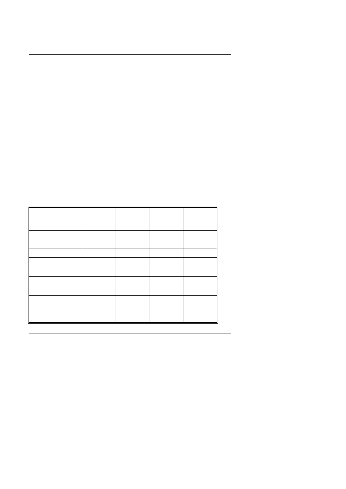
1.3. PERFORMANCE LIST
The following list of performance data is the testing results of some popular
benchmark testing programs.
These data are just referred by users, and there is no responsibility for different
testing data values gotten by users. (The different Hardware & Software configuration
will result in different benchmark testing results.)
• CPU
Pentium Processor MMX-233 MHz, Cyrix 6x86MXPR333, AMD K6-3 400, AMD K6-2 450
• DRAM (32 × 3) MB SDRAM (MICRON MT48LC2M8A-8)
• CACHE SIZE 512 KB
• DISPLAY Onboard SIS530 AGP Card
• STORAGE Onboard IDE (Seagate ST34520A)
• O.S. Windows® NT 4.0
• DRIVER
Processor
Winbench99
CPU mark32
FPU Winmark
Business Disk
Hi-End Disk
Business Graphics
Hi-End Graphics
Display Driver at 1024 x 768 x 64K colors x 75Hz.
SIS Bus Master IDE Driver
Intel-MMX
233MHz
(66x3.5)
AMD K6-2
450
(100x4.5)
AMD K6-3
400
(100x4)
312 555 1220 470
876 1480 1360 573
3270 3750 4320 3680
8280 9520 10500 9520
53.8 82.9 111 89.1
106 199 319 187
Winstone99
Business
Hi-End
13.1 20.2 27 19.1
11.4 18.5 23.9 14.6
Cyrix 6x86MX-
PR333
(83x3 )
1-3
Page 6
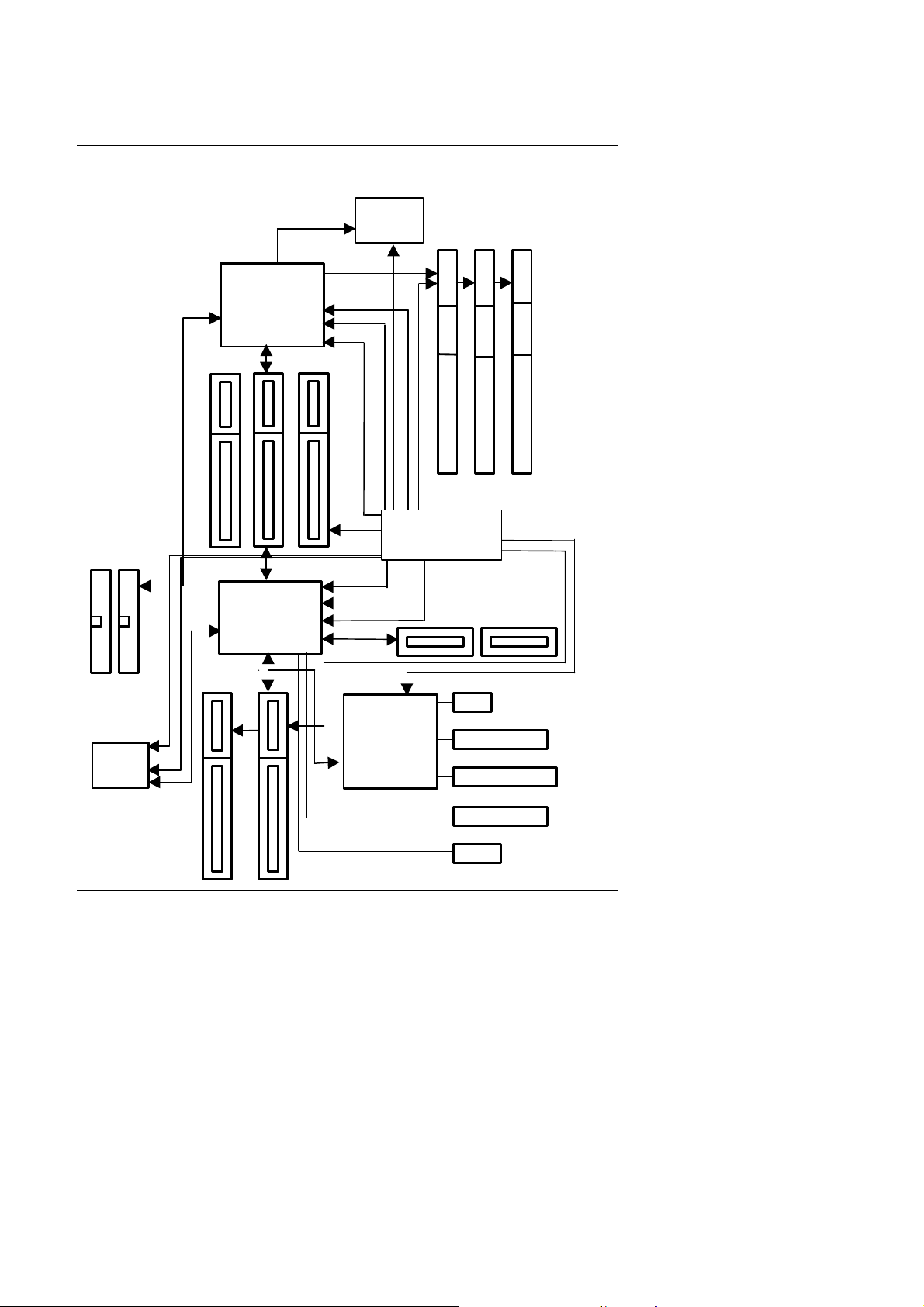
1.4. BLOCK DIAGRAM
Introduction
IDE BUS
Ultra DMA/33
IDE Ports
33MHz
SOLO1
14.318
MHz
ISA Bus
SiS
530
CHIPSET
SiS
5595
CHIPSET
HOST Bus
DRAM Bus
33MHz
66~100 MHz
66~100
MHz
33 MHz
33 MHz
48MHz
14.318MHz
USB Bus
14.318MHz
CHIPSET
ITE 8661
CPU
I/O
3.3V SDRAM
DIMM Sockets
CLOCK
GEN
24MHz
COM Ports
LPT Port
Floppy Port
PCI Bus
Keyboard
PS/2 Mouse
1-4
Page 7

5SMM
1.5. INTRODUCE THE PCI - BUS
Connecting devices to a CPU local bus can dramatically increase the speed of I/Obound peripherals with only a slight increase in cost over traditional systems.
This price / Performance point has created a vast market potential for local bus
products.
The main barrier to this market has been the lack of an accepted standard for local
bus peripherals.
Many mainboard and chipset manufactures developed their own local bus
implementations, but they are incompatible with each other.
The VL (Video Electronics Standards Association) local bus and PCI (Peripheral
Component Interconnect) bus specification was created to end this confusion.
The PCI - bus standard, under development since Jun. 1992, which is designed to
bring workstation-level performance to standard PC platform. The PCI - bus removes
many of the bottlenecks that have hampered PC for several years.
On the PCI - bus, peripherals operate at the native speed of the computer system,
thus enabling data transfer between peripherals and the system at maximum speed.
This performance is critical for bandwidth-constrained devices such as video,
multimedia, mass storage, and networking adapters.
PCI - bus standard provides end-users with a low-cost, extendible and portable local
bus design, which will allow system and peripherals from different manufactures to
work together.
1.6. FEATURES
32 bits bus transfer mode.
q
Bus Master or Slave access.
q
Memory burst transfer to 132 MB/sec.
q
33 MHz operation speed.
q
10 device loading ability.
q
CPU independent.
q
1-5
Page 8

Page 9

2. SPECIFICATION
2.1. HARDWARE
•
CPU
•
COPROCESSOR −
•
SPEED −
•
DRAM MEMORY −
•
CACHE MEMORY −
•
I/O BUS SLOTS −
•
IDE PORTS −
Pentium Processor
−
133 / 166 / 200 MHz ; MMX(166 / 200 / 233)
− AMD
K6 (166 / 200 / 233 / 266 / 300)
K6-2 (266 / 300 / 333 / 350 / 366 / 380 / 400 / 450
/ 475 / 500 / 550)
K6-III (400 / 450 /475 / 500 / 550)
− Cyrix / IBM
6x86MX (PR166 / PR200 / PR233 / PR266)
M¢º-PR300 / PR333 / PR350 / PR366 / PR400
− IDT
Winchip 2-(200 / 225 / 233 / 266 / 300)
Winchip 3-(266)
− RISE
MP6-(266)
321 pins (socket 7) ZIF white socket on board.
−
1.3V-3.5V Dual Power Ready.
−
Included in processor.
66 / 75 / 83 / 90 / 95 / 100MHz system speed.
33 MHz PCI-Bus speed.
−
8 MHz AT bus speed.
−
3 banks 168 pins DIMM module socket on board.
− Use 16 / 32 / 64 / 128 / 256 MB DIMM module
DRAM.
16 ~ 768 MB DRAM size.
−
Onboard 8MB SDRAM. (Optional)
−
16 / 24 / 32 / 64KB L1cache included in CPU.
512 KB 2nd Level cache on board.
−
Supports Write Back cache function for both CPU
−
& on board cache.
3 xMaster / Slave PCI-BUS Slots.
2 x16 bits ISA BUS Slots.
−
2-channel Enhanced IDE port on board.(Using
IRQ14,15)
Supports Mode 3,4 IDE & ATAPI CD – ROM.
−
Supports Ultra DMA 33 / 66.
−
Specification
2-1
Page 10

5SMM
•
•
I/O PORTS −
• Audio Ports
(Optional)
GREEN FUNCTION −
•
BIOS −
•
SOUND −
•
DIMENSION −
2.2. SOFTWARE
• BIOS
• O.S.
Supports 1 x16550 COM ports. (Using IRQ4, 3)
Supports 1 x EPP/ECP LPT port. (Using IRQ7 or 5
−
and DMA3)
Supports 1 x 1.44/2.88 MB Floppy port. (Using
−
DMA2 & IRQ6)
Supports PS/2 Mouse. (Using IRQ12 )
−
− 1x Line in
− 1x Line out
− 1x Micro in
− 1x Game Port
− 2x CD Line in
− 1x TEL
Suspend mode support.
Green switch & Green LED support.
−
IDE & Display power down support.
−
Monitor all IRQ / DMA / Display / I/O events.
−
2Mbit FLASH RAM.
Supports Plug & Play Function.
−
Onboard ESS SOLO-1 ES1938S PCI Sound.
Micro ATX Form Factor, 4 layers PCB.
Licensed AWARD BIOS.
−
AT CMOS Setup, BIOS / Chipset Setup, Green
−
Setup, Hard Disk Utility included.
Operation with MS-DOS, Windows95,
−
Windows98, WINDOWS NT, OS/2, NOVELL
and SCO UNIX.
2.3. ENVIRONMENT
• Ambient Temp.
• Relative Hum.
• Altitude
• Vibration
• Electricity
0°C to +50°C (Operating).
−
0 to +85% (Operating).
−
0 to 10,000 feet (Operating).
−
0 to 1,000 Hz.
−
4.9 V to 5.2 V.
−
Max. 20A current at 5V.
−
2-2
Page 11

3. HARDWARE INSTALLATION
3.1. UNPACKING
The mainboard package should contain the following:
• The 5SMM mainboard.
• USER’ S MANUAL for mainboard.
Hardware Installation
• Cable set for IDE
¡B
Floppy.
• CD for Mainboard Utility.
The mainboard contains sensitive electric components which can be easily damaged
by static electricity, so the mainboard should be left in its original packing until it is
installed.
Unpacking and installation should be done on a grounded anti-static mat.
The operator should be wearing an anti static wristband, grounded at the same point
as the anti-static mat.
Inspect the mainboard carton for obvious damage. Shipping and handling may cause
damage to your board. Be sure there are no shipping and handling damage on the
board before proceeding.
After opening the mainboard carton, extract the system board and place it only on a
grounded anti-static surface component side up. Again inspect the board for damage.
Press down on all of the socket IC’ s to make sure that they are properly seated. Do
this only on with the board placed on a firm flat surface.
M
DO NOT APPLY POWER TO THE BOARD IF IT HAS BEEN DAMAGED.
It is assumed that the chassis is designed for a standard ATX 2.0 mainboard
mounting. Place the chassis on the anti-static mat and remove the cover.
Take the plastic clips, Nylon stand-off and screws for mounting the system board,
and keep them separate.
3-1
Page 12

5SMM
ISA 1
ISA 2
PCI 1
PCI 3
PCI 2
3.2 MAINBOARD LAYOUT
BIOS
ESS
SOLO-1
ES1938S
5595
BAT 1
J10
SYSTEM
FAN
GAME &
Audio
JP7
VGA
SW 1
5SMM
IDE 2
IDE 1
SIS530
LPT
COM A
ATX POWER
USB
JP3
CPU
FLOPPY
×Figure 3.1Ø
3.3. QUICK REFERENCE FOR JUMPERS & CONNECTORS
I/O Ports Connector
t
IDE 1 For Primary IDE port.
IDE 2 For Secondary IDE port.
Floppy For Floppy port.
USB For USB port.
COM A For Serial port1 (COM A).
VGA For VGA port.
GAME For GAME port.
AUDIO For MIC,LINE-IN,LINE-OUT port.
LPT For LPT port.
PS/2 For PS/2 Mouse & Keyboard Connector.
ATX Power For ATX Power Connector.
PS/2
J9
JP2
SW2
3-2
Page 13

t JP4: Wake on Lan
Pin Function
1 +5V SB
2 GND
3 Signal
t JP5 :Internal MODEN WAKE UP
Pin Function
1 Signal
2 GND
t FAN1: CPU cooling FAN Power Connector
Pin Function
1 GND
2 +12V
3 Signal
t JP2: Keyboard Power On Connector
Pin Function
1,2 Close Enabled Keyboard power on.
2,3 Close Disabled Keyboard power on.
Hardware Installation
t FAN2 : SYSTEM FAN
Pin Function
1 GND
2 +12V
3 Signal
t JP7 : CLEAR CMOS
Pin Function
1-2 CLEAR CMOS
2-3 Normal
3-3
Page 14

5SMM
t JP1 : On-Board Sound Function Connector
Pin No. Function
1-2 Enabled On-Board Sound Function.
2-3 Disabled On-Board Sound Function.
t JP3 : Infrared Connector (Optional)
Pin No. Function
1 IR Data Output
2 GND
3 IR Data Input
4 NC
5 Power (+)
t J9 : PS/2 Mouse by Connector (Optional)
Pin Function
1 VCC
2 GND
3 Data
4 Clock
t J10 : TEL:The Connector is for Modem with internal Voice connector
Pin Function
1 Signal
2 GND
3 GND
4 Signal
t J1 : CD Audio Line In
Pin Function
1 GND
2 Right
3 GND
4 Left
3-4
Page 15

t J2 : CD Audio Line In
Pin Function
1 Right
2 GND
3 GND
4 Left
J4 : 2*11 PIN Jumper
PW
Hardware Installation
P+P− P−
J4
1
RE SPK
PW : Soft Power Connector
On – Off : For POWER ON or Suspend IN / OUT.
On 4 sec : For POWER OFF before VGA Enable or
RE : Reset Switch
Open: Normal Operation
Short: For Hardware Reset System
P+P− P−: Power LED
1
SPK: Speaker Connector
+
1
PIN 1: anode (+)
PIN 2: cathode (−)
PIN 3: cathode (−)
−
PIN 1: VCC
PIN 2: NC
PIN 3: NC
1 1
1
GNGD
HD
CMOS setup select “delay 4sec.” for
POWER OFF mode.
3-5
Page 16

5SMM
PIN 4: Data
HD: IDE Hard Disk Active LED
1
PIN 1: LED anode (+)
PIN 2: LED cathode (−)
GN: Green Switch
Open: Normal operation
Short: Entering Green Mode
GD: Green Function Active LED
PIN 1: LED athode (+)
1
PIN 2: LED cathode (−)
3.4. SRAM INSTALLATION
Sync. SRAM (Pipeline Burst SRAM)
If Sync SRAM Chip is installed, it consists of Pipeline Burst 1 Pc 64 K x 64 512KByte.
3.5. DRAM INSTALLATION
The mainboard can be installed with 16 / 32 / 64 / 128 / 256 MB 168 pins DIMM
module DRAM, and the DRAM speed must be 67~100 MHz for SDRAM. The DRAM
memory system on mainboard consists of bank 0 & bank1¡Bbank2 .
Because the 168 pins DIMM module is 64 bits width, using 1 PCS which can match a
64 bits system. The total memory size is 16 MB ~ 768 MB DRAM. The DRAM
installation position refer to Figure 3.1, and notice the Pin 1 of DIMM module must
match with the Pin 1 of DIMM socket. Insert the DRAM DIMM module into the DIMM
socket at Vertical angle. If there is a wrong direction of Pin 1, the DRAM DIMM
module couldn't be inserted into socket completely.
3-6
Page 17

Hardware Installation
3.6. CPU INSTALLATION AND JUMPERS SETUP
The system speed depends on the frequency of CLOCK GENERATOR. The user can
change SW selection to set up the system speed to 66 / 75 / 83 / 90 / 95 / 100MHz
for 3.3V/2.5V Pentium Processor (133 / 166 / 200 MHz) ;MMX(166 / 200 / 233
MHZ) , AMD K6-(166 / 200 / 233 / 266 / 300 ; K6-2(266 / 300 / 333 / 350 / 366 / 380
/ 400 / 450 / 475 / 500 / 550) ; K6-III(400 / 450 / 475 / 500 / 550) , Cyrix / IBM
6x86MX (PR166 / PR200 / PR233 / PR266 ) ; M¢º- PR300 / PR333 / PR350 /
PR366 / PR400) ; IDT Winchip 2-(200 / 225 / 233 / 266 / 300) ; IDT Winchip 3-(266) ;
RISE MP6-(266).
The mainboard can use Pentium Processor, MMX , AMD-K6, AMD-K6-2, AMD-K6III Cyrix / IBM 6x86MX, Cyrix M¢º, IDT Winchip 2 , IDT Winchip 3 , RISE MP6 CPU,
and the CPU speed must match with the frequency of CLOCK GEN. It will cause
system hanging up if the CLOCK GEN.'S frequency is faster than CPU's.
M
The CPU is a sensitive electric component and it can be easily damaged by
static electricity, so users must keep it away from metal surface when the
CPU is installed onto mainboard.
M
When the user installs the CPU on socket, please notice that the PIN 1 of
CPU is in the same corner as the PIN 1 of socket!
M
Before the CPU is installed, the mainboard must be placed on a flat plane
in order to avoid being broken by the pressure of CPU installation.
SW: CPU INT./ EXT. FREQ. RATIO
O: ON
X: OFF
SW2 4 5 6 7 8 SW2 4 5 6 7 8
1.3V
1.4V
1.5V
1.6V
1.7V
1.8V
1.9V
2.0V
2.1V
2.2V
2.3V
X X X X O
X O X X O
X X O X O
X O O X O
X X X O O
X O X O O
X X O O O
X O O O O
O X X X X
X O X X X
O O X X X
3-7
2.5V
2.6V
2.7V
2.8V
2.9V
3.0V
3.1V
3.2V
3.3V
3.4V
3.5V
O X O X X
X O O X X
O O O X X
X X X O X
O X X O X
X O X O X
O O X O X
X X O O X
O X O O X
X O O O X
O O O O X
Page 18

5SMM
2.4V
X X O X X
---
--- --- --- --- ---
SW2 1 2 3
X1.5
X2
X2.5
X3
X3.5
X4
X4.5
X5
X5.5
X X X
O X X
O O X
X O X
X X X
O X O
O O O
X O O
X X O
SW 1 :
CPU SDRAM PCI 1 2 3 4
66.8 66.8 33.4 O O O X
75 75 30 X O O X
83.3 83.3 33.3 O X O X
95 95 31.7 X X O X
100 100 33.4 O O X X
112 112 37.3 X O X X
124 124 31 O X X X
133 133 33.3 X X X X
90 90 30 O O O O
♦Note: If Cyrix 6x86 is being used, please check the CPU Date Code after 605.
♦Note: It’ s strongly recommended that set the system speed according to your hardware
configuration: CPU, SDRAM, Cards, etc.
3.7. CMOS RTC & ISA CFG CMOS SRAM
Built-in Real Time Clock (RTC) With 256B CMOS SRAM in SIS 5595.
3-8
Page 19

Hardware Installation
3.8. SPEAKER CONNECTOR INSTALLATION
There is a speaker in AT system for sound purpose. The 4 - Pins connector SPK is
used to connect speaker. The speaker can work well in both direction of connector
when it is installed to the connector SPK on mainboard.
3.9. HARDWARE RESET SWITCH CONNECTOR INSTALLATION
The RESET switch on panel provides users with HARDWARE RESET function which
is almost the same as power-on/off. The system will do a cold start after the RESET
switch is pushed and released by user. The RESET switch is a 2 PIN connector and
should be installed to RE on mainboard.
3.10. GREEN FUNCTION INSTALLATION
There is one jumper for the purpose of power saving, GN, to indicate the power
saving function . If the GD is lighted on, the system is in green mode. The GN switch
will force the system into green mode .
3.11. PERIPHERAL DEVICE INSTALLATION
After installation of the device and setup of the jumpers, the mainboard can be
mounted into the case and fixed by screw. To complete the mainboard installation,
the peripheral devices could be installed now. The basic system needs a display
interface card and a storage device.
If a PCI - Bus device is to be installed in the system, any one of three PCI - Bus slots
can be used for Slave or Master PCI - Bus device.
After installing the peripheral device, the user should check everything again and
prepare to power-on the system.
3-9
 Loading...