GHI LQFP144, LQFP100 User Manual
G H I E l e c t r o n i c s
USBizi User Manual
Rev. 4.4 March 10, 2011 User Manual
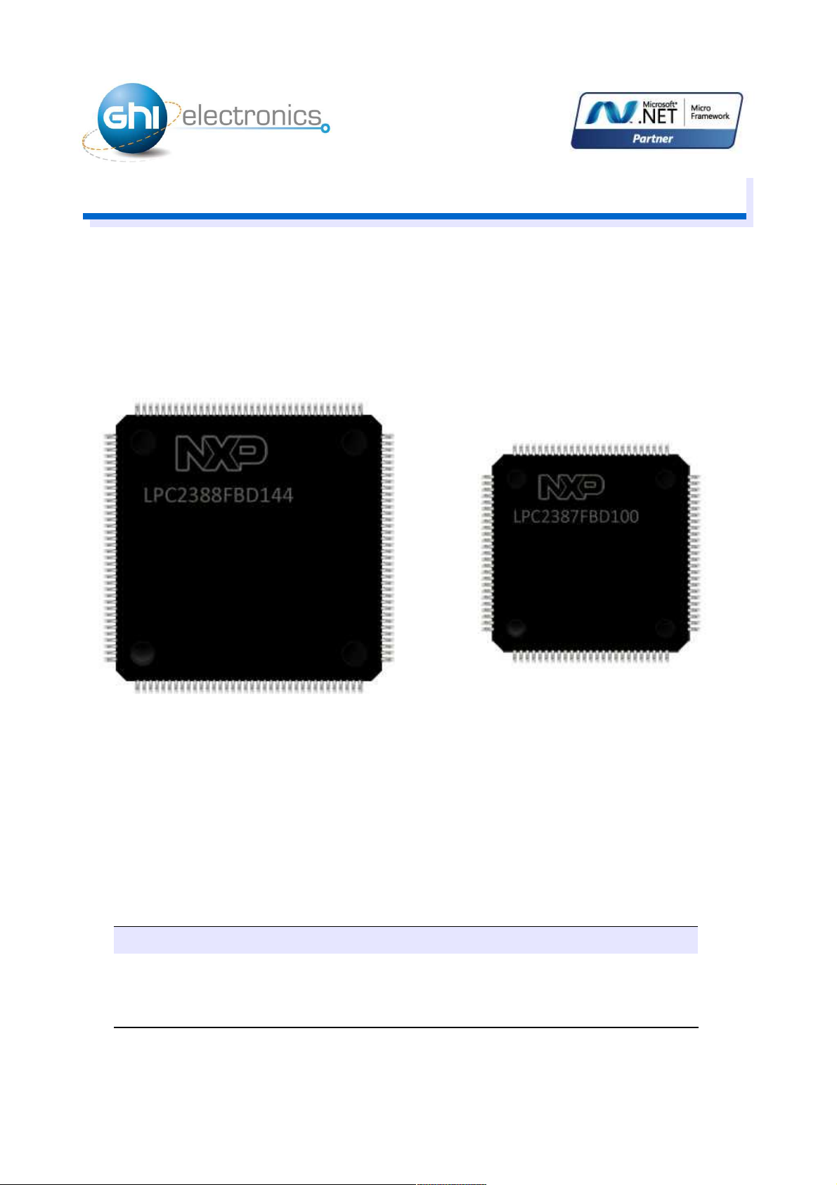
USBizi Chipset LQFP144 USBizi Chipset LQFP100
Document Information
Information Description
Abstract This document covers information about USBizi Chipset,
specifications, tutorials and references.
GHI Electronics,LLC USBizi User Manual
Rev. 4.4 Page 2 of 38 www.ghielectronics.com
Revision History
Date Modification
03/10/11 Added RLP
10/14/10 Native Ethernet TCP/IP support using W5100 (WIZnet Hardwired
TCP/IP Embedded Ethernet Controller)
09/14/10 Added in-field update section
07/21/10 Updated information for NETMF 4.1
07/12/10 Added more pins
05/18/10 Added more pins
03/05/10 Various modifications
03/03/10 First version

GHI Electronics,LLC USBizi User Manual
Table of Contents
Table of Contents
1.Introduction...................................................................................4
1.1.What is Microsoft .NET Micro Framework (NETMF)?.........4
1.2.NETMF - Porting vs. Using..................................................4
1.3.GHI's .NET Micro Framework Based Solutions..................5
1.4.What is USBizi Chipset?.....................................................5
1.5.Block Diagram.....................................................................6
1.6.USBizi Chipset Key Features..............................................6
1.7.Example Applications..........................................................6
2.Pin-Out Description.......................................................................7
2.1.USBiziTM LQFP 144 Pin-out Table.....................................8
2.2.USBiziTM LQFP 100 Pin-out Table...................................11
3.USBizi On boot up......................................................................14
3.1.GHI Boot Loader vs. USBizi Firmware..............................14
3.2.Boot up Modes Settings and Access Interface Drivers.....15
4.GHI Boot Loader.........................................................................16
4.1.GHI Boot Loader Commands............................................16
4.2.USBizi Firmware Update...................................................17
4.3.Managed (User) Application in Production Stage with Copy
Protection.................................................................................18
5.USBizi Firmware.........................................................................19
5.1.Getting Started with USBizi...............................................19
All you need to start up.....................................................19
First Power-up...................................................................19
Adding GHI NETMF Library..............................................23
5.2.Recommended Hardware and Tutorials for USBizi .........25
6.USBizi Features..........................................................................27
6.1.Application Flash/RAM......................................................27
6.2.Debugging Interface (Access Interface)............................27
6.3.Digital Inputs/Outputs........................................................28
6.4.Serial Peripherals..............................................................28
Serial Port (UART)............................................................28
SPI.....................................................................................28
I2C.....................................................................................29
CAN...................................................................................29
One-wire Interface.............................................................29
6.5.Networking.........................................................................29
Ethernet.............................................................................29
6.6.Graphics............................................................................29
6.7.USB Client (Device) ..........................................................31
USB Cable Connection Detection.....................................32
6.8.USB Host and Supported Class Drivers...........................33
6.9.Storage Devices (SD, USB MS) / File System..................33
SD/MMC Memory..............................................................33
USB Mass Storage............................................................34
6.10.Analog Inputs/Outputs.....................................................34
6.11.PWM................................................................................34
6.12.Output Compare..............................................................34
6.13.Battery RAM....................................................................34
6.14.Power Control / Hibernate...............................................35
Power Control....................................................................35
Hibernate...........................................................................35
6.15.Real Time Clock..............................................................35
6.16.Processor Register Access.............................................35
6.17.In-Field Update................................................................35
6.18.Managed Application Protection......................................36
6.19.Runtime Loadable Procedure (RLP)...............................36
6.20.Watchdog.........................................................................36
7.Advanced Users..........................................................................37
8.USBizi Design Consideration......................................................37
Legal Notice...................................................................................38
Licensing..................................................................................38
Disclaimer................................................................................38
Rev. 4.4 Page 3 of 38 www.ghielectronics.com

GHI Electronics,LLC USBizi User Manual
Introduction
1. Introduction
1.1. What is Microsoft .NET Micro Framework (NETMF)?
Microsoft .NET Micro Framework is a lightweight implementation of .NET Framework. It
focuses on the specific requirements of resource-constrained embedded systems.
Supporting development in C# and debugging on an emulation or the device, both using
Microsoft's Visual Studio. The .NET Micro Framework is also open source, released under
the Apache 2.0 license and completely free.
Developers already experienced with .NET and Visual Studio can take advantage of their
skills immediately reducing the learning curve. The actual C# application development
process is completely shielded from the low-level design details of the hardware platform.
Combining the benefits with off-the-shelf, low-cost, network-enabled embedded systems
creates a rapid product development solution.
1.2. NETMF - Porting vs. Using
There are two sides to working with NETMF, porting it and using it. For example, writing a
JAVA game on a cell phone is much easier than porting the JAVA virtual machine (JVM) to
the phone. The phone manufacturer did all the hard work of porting JAVA to their phone
allowing the game programmers to use it with ease. NETMF works the same way, porting
is not easy but using it is effortless.
NETMF can be split into two major components, the core (CLR) and HAL (Hardware
Access Layer). The core libraries are made so they are hardware independent. Usually, no
modifications are needed on the core libraries. A developer porting NETMF for a hardware
platform will need to make the HAL to handle interfacing the hardware control to upper
layers.
According to GHI's experience with NETMF porting, it is not feasible to work on porting
NETMF to your new hardware in case you are targeting medium or low quantities annually
(less than 100,000 units). A faster-to-market option is by using one of the available OEM
modules/chipsets. These OEM devices have everything you need built in the hardware
and software.
Rev. 4.4 Page 4 of 38 www.ghielectronics.com
GHI Electronics,LLC USBizi User Manual
Introduction
1.3. GHI's .NET Micro Framework Based Solutions
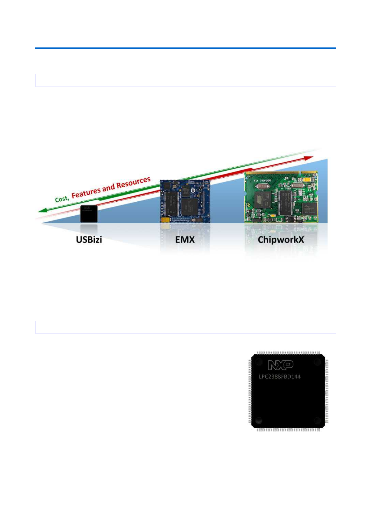
With GHI Electronics, you're getting an experienced partner that offers a wide range of
.NET Micro Framework hardware and software capabilities using the various drop-in
modules/chipsets such as ChipworkX, Embedded Master, EMX and USBizi. In addition,
our free unlimited support is available to assist you at any point. New features and fixes
come seamlessly to your product at no cost to you.
On top of the great features that .NET Micro Framework provides, such as Ethernet,
graphics and touch screen, GHI solutions has additional exclusive features such as USB
host, PPP (GPRS/3G), database and native code runtime libraries (RLP). All these
exclusive features are included at no extra cost to you.
1.4. What is USBizi Chipset?
USBizi Chipset, pronounced as USB easy, is an ARM7
microcontroller from NXP (LPC2388 or LPC2387) with a
special firmware developed to host .NET Micro Framework
with various HAL drivers. With this sophisticated
combination, a developer can easily control this
microcontroller IOs and interfaces such as SPI, UART(Serial
Port) and I2C with simple unified managed code (C# code)
and enjoy the wide various higher level services offered by
NETMF such as file system access. Not to mention GHI's
extended features such as PWM, ADC, DAC and Full USB
host stack. Everything implemented on a single-chip making
USBizi the smallest and most inexpensive .NET Micro
Framework device, and still implements unique features like
USB host.
Rev. 4.4 Page 5 of 38 www.ghielectronics.com
GHI Electronics,LLC USBizi User Manual
Introduction
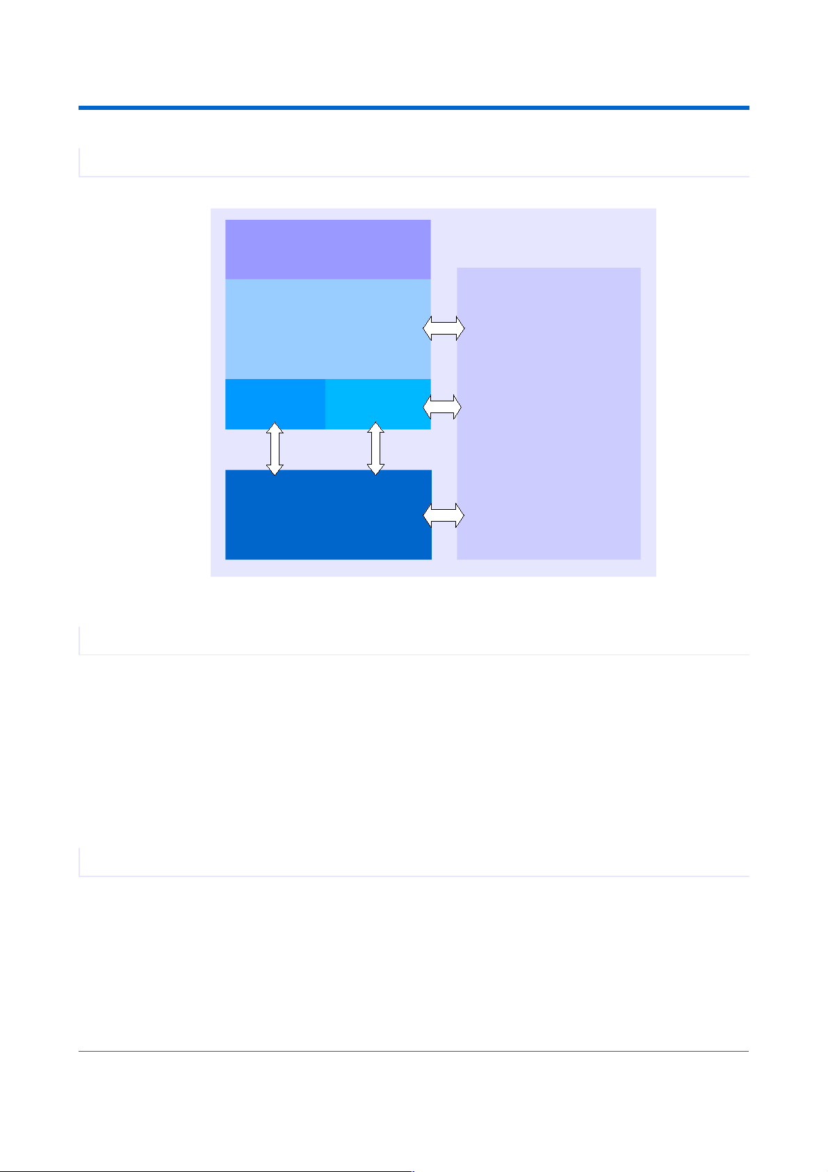
1.5. Block Diagram
1.6. USBizi Chipset Key Features
● Microsoft .NET Micro Framework V4
● 72Mhz 32-bit Processor
● 96KB RAM
● 0.5MB FLASH
● Embedded USB Host(144 pin package only)
● Embedded USB Client (Device)
● 71 GPIO
● 35 Interrupt Inputs
● 2 SPI (8/16bit)
● I2C
● 4 UART
● 2 CAN Channels
● 8 10-bit Analog Inputs (6 on 100pin package)
● 10-bit Analog Output
● 4-bit SD/MMC interface
● 6 PWM
● 100 mA everything enabled
● 200 uA Hibernate Modes
● -40ºC to +85ºC Operational
● RoHS Lead Free
1.7. Example Applications
● Data logger.
● MP3 player.
● Measurement tool or tester.
● Robotics.
● GPS navigation.
● Medical instrumentation.
● Industrial automation devices.
Rev. 4.4 Page 6 of 38 www.ghielectronics.com
LPC2388/87
72 MHz ARM7
with 512KB Flash Memory
and 96KB RAM
Peripherals
GPIO, Interrupts, PWM, A/D,
USB HC, USB Device,
MCI,LCD Controller,
Ethernet Controller ...etc
GHI Extended features:
USB Drivers, Hardware Access
USBizi Chipset
Hardware
.NET Micro Framework
CLR
HALPAL
.NET and GHI
Managed Library

GHI Electronics,LLC USBizi User Manual
Pin-Out Description
2. Pin-Out Description
USBizi Chipset is based on LPC2388 or LPC2387 72Mhz ARM7 32-bit processor. The
processor has a wide range of peripherals that adds a lot of functions and features to
USBizi such as PWM, GPIO, USB HC ...etc.
Most signals on USBizi are multiplexed to offer more than one function for every pin. It is
up to the developer to select which one of the functions to use. GHI drivers and .NET
Micro Framework does checking to make sure the user is not trying to use two functions
on the same pin. The developer should still understand what functions are multiplexed so
there is no conflict. For example, analog channel 3 (ADC3) and the analog output (AOUT)
are on the same pin IO22. Either function can be used but not both of them
simultaneously. Visit Advanced Users section.
• Pins not mentioned cannot be accessed directly, however, they can be used using
the Register class provided by the GHI native library. Visit Advanced Users
section.
• The schematics of USBizi boards should be used as a reference design. The
boards are USBizi Development System, FEZ Domino and FEZ Mini.
• Advanced details on oscillator and power tolerance can be found in the LPC2388
datasheet from NXP website.
• Digital I/O pins are named IOxx, where xx is an assigned number.
Rev. 4.4 Page 7 of 38 www.ghielectronics.com
GHI Electronics,LLC USBizi User Manual
Pin-Out Description
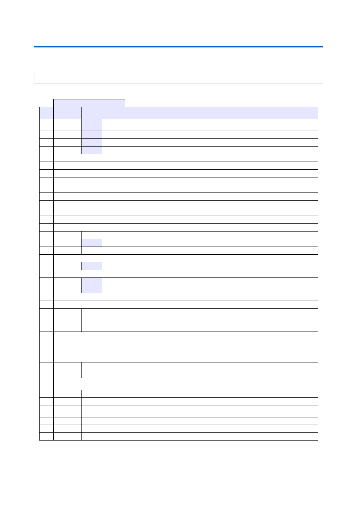
2.1. USBiziTM LQFP 144 Pin-out Table
USBizi LQFP144 chipset is based on LPC2388 from NXP.
Name * Interrupt capable input.
No. LPC2388
H/W
USBizi IO2
nd
Feature
USBizi
Pin Description
8 P0.26 IO22* ADC3/
DAC
ADC3 (10-Bit Analog to Digital Input) or DAC (Digital to Analog Output)
10 P0.25 IO24* ADC2 ADC2 (10-Bit Analog to Digital Input)
11 P0.24 IO26* ADC1 ADC1 (10-Bit Analog to Digital Input)
13 P0.23 IO28* ADC0 ADC0 (10-Bit Analog to Digital Input)
14 VDDA Connect to 3.3 volt source
15 VSSA Connect to Ground
17 VREFA Connect to 3.3 volt source
18 VDD_1 Connect to 3.3 volt source
22 VSS1 Connect to Ground
23 RTCX1 Connect to real-time crystal circuit pin 1
24 RESET# Hardware reset signal, Reset state is on Low
25 RTCX2 Connect to real-time crystal circuit pin 2
26 ALARM The alarm pin is an RTC controlled output. This is a 1.8 V pin.
27 VBAT Connect to 3.3 volt back up battery to keep the real-time clock running.
28 P1.31 IO32 ADC5 ADC5 (10-Bit Analog to Digital Input)
29 P0.12 IO30* ADC6 ADC6 (10-Bit Analog to Digital Input)
30 P1.30 IO29 ADC4 ADC4 (10-Bit Analog to Digital Input)
31 XTAL1 Connect to the system's 12MHz. crystal pin1
32 P0.13 IO27* ADC7 ADC7 (10-Bit Analog to Digital Input)
33 XTAL2 Connect to the systems 12MHz. crystal pin1
34 P0.28 IO31* I2C (open drain pin) I2C Interface SCL
35 P0.27 IO33* I2C (open drain pin) I2C Interface SDA
36 USBD+ USB Client Feature USB positive data line, USB (access) debugging interface and for the USB client feature.
37 USBD- USB Client Feature USB negative data line, USB (access) debugging interface and for the USB client feature.
38 P3.26 IO69 N/A General purpose digital I/O
39 P3.25 IO68 N/A General purpose digital I/O
39 P3.24 IO70 N/A General purpose digital I/O
41 VDD1 Connect to 3.3 volt source
42 USBD+ USB Host Feature USB positive data line of the USB hosting feature.
43 USBD- USB Host Feature USB negative data line of the USB hosting feature.
44 VSS2 Connect to Ground
46 P1.18 IO35 PWM1 PWM1 (Pulse Width Modulation Output)
47 P1.19 IO34 N/A General purpose digital I/O
48 USB_CON USB Client Feature Reports the USB cable attachment to the PC USB Host (refer to the reference design
schematic for the required circuit).
49 P1.20 IO25 PWM2 PWM2 (Pulse Width Modulation Output)
50 P1.21 IO23 PWM3 PWM3 (Pulse Width Modulation Output)
51 P1.22 IO61 USB_PW
R_RD
Related to USB host feature (refer to the reference design schematic for connection)
53 P1.23 IO62 N/A General purpose digital I/O
54 P1.24 IO63 N/A General purpose digital I/O
56 P1.25 IO64 N/A General purpose digital I/O
Rev. 4.4 Page 8 of 38 www.ghielectronics.com
GHI Electronics,LLC USBizi User Manual
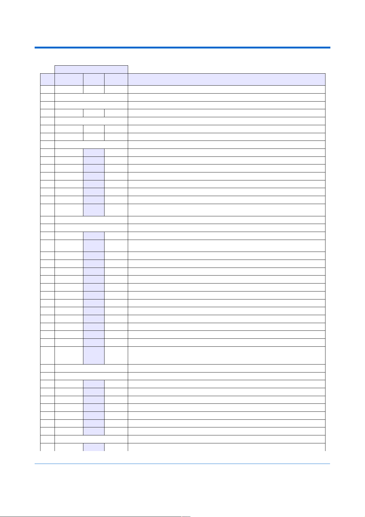
Pin-Out Description
Name * Interrupt capable input.
No. LPC2388
H/W
USBizi IO2
nd
Feature
USBizi
Pin Description
57 P1.26 IO65 N/A General purpose digital I/O
59 VSS3 Connect to Ground
60 VDD_2 Connect to 3.3 volt source
61 P1.27 IO21 N/A General purpose digital I/O
62 VDD2 Connect to 3.3 volt source
63 P1.28 IO66 N/A General purpose digital I/O
64 P1.29 IO67 N/A General purpose digital I/O
65 VSS4 Connect to Ground
66 P0.0 IO19* CAN1 RD CAN Channel 1 Data Receive pin (In)
67 P0.1 IO15* CAN1 TD CAN Channel 1 Data Transmit pin (Out)
69 P0.10 IO39* N/A Only general purpose digital I/O
70 P0.11 IO38* N/A Only general purpose digital I/O
71 P2.13 IO50* SD_DAT3 SD card 4-bit data bus, data line no. 3
73 P2.12 IO49* SD_DAT2 SD card 4-bit data bus, data line no. 2
75 P2.11 IO48* SD_DAT1 SD card 4-bit data bus, data line no. 1
76 P2.10 IO0* BL# General purpose digital I/O. On power up, this pin is used to access GHI boot loader
when Low (refer to GHI boot loader section).This pin is high (no loader) if not connected.
77 VDD3 Connect to 3.3 volt source
79 VSS5 Connect to Ground
80 P0.22 IO47* SD_DAT0 SD card 4-bit data bus, data line no. 0
82 P0.21 IO46* MCIPWR Memory card (SD/MMC) power enable signal (refer to the reference design schematic for
connection).
83 P0.20 IO45* SD_CMD SD card 4-bit data bus, command line
85 P0.19 IO44* SD_CLK SD card 4-bit data bus, clock line
86 P0.18 IO41* SPI1 SPI master bus interface MOSI signal (Master Out Slave In) for SPI1
87 P0.17 IO40* SPI1 SPI master bus interface MISO signal (Master In Slave Out)for SPI1
89 P0.15 IO42* SPI1 SPI master bus interface SCK signal (Clock)for SPI1
90 P0.16 IO43* N/A General purpose digital I/O
92 P2.9 IO37* COM3 Serial port (UART) RXD receive signal (In) for COM3
93 P2.8 IO36* COM3 Serial port (UART) TXD transmit signal (Out) for COM3
95 P2.7 IO11* COM2 Serial port (UART) RTS signal for COM2
96 P2.6 IO9* N/A Only general purpose digital I/O
97 P2.5 IO7* PWM6 PWM6 (Pulse Width Modulation Output)
99 P2.4 IO2* PWM5 PWM5 (Pulse Width Modulation Output)
100 P2.3 IO4* PWM4/M
ODE
PWM4 (Pulse Width Modulation Output). On power up, this pin is used to select the
access interface for GHI boot loader and debugging, between USB (High) or COM1(Low).
(refer to GHI boot loader section). This pin is high (select USB) if not connected.
102 VDD4 Connect to 3.3 volt source
103 VSS6 Connect to Ground
105 P2.2 IO1* COM2 Serial port (UART) CTS signal for COM2
106 P2.1 IO3* COM2 Serial port (UART) RXD receive signal (In) for COM2
107 P2.0 IO5* COM2 Serial port (UART) TXD transmit signal (Out) for COM2
109 P0.9 IO6* SPI2 SPI master bus interface MOSI signal (Master Out Slave In) for SPI2
111 P0.8 IO8* SPI2 SPI master bus interface MISO signal (Master In Slave Out)for SPI2
112 P0.7 IO10* SPI2 SPI master bus interface SCK signal (Clock)for SPI2
113 P0.6 IO12* N/A General purpose digital I/O
114 VDD5 Connect to 3.3 volt source
115 P0.5 IO14* CAN2 TD CAN Channel 2 Data Transmit pin (Out)
Rev. 4.4 Page 9 of 38 www.ghielectronics.com
GHI Electronics,LLC USBizi User Manual
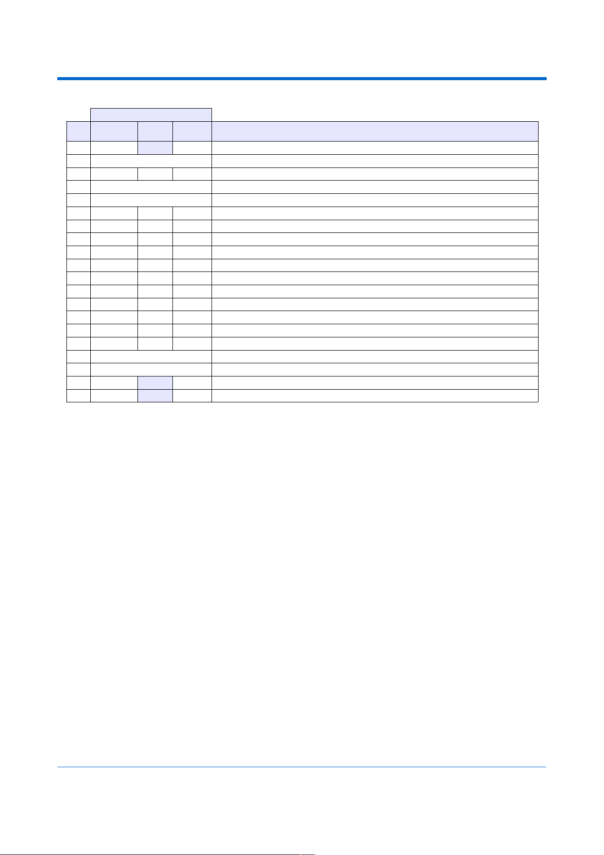
Pin-Out Description
Name * Interrupt capable input.
No. LPC2388
H/W
USBizi IO2
nd
Feature
USBizi
Pin Description
116 P0.4 IO16* CAN2 RD CAN Channel 2 Data Receive pin (In)
117 VSS7 Connect to Ground
118 P4.28 IO13 COM4 Serial port (UART) TXD transmit signal (Out) for COM4
119 VSS8 Connect to Ground
121 VDD_3 Connect to 3.3 volt source
122 P4.29 IO17 COM4 Serial port (UART) RXD receive signal (In) for COM4
123 P1.17 IO60 N/A General purpose digital I/O
125 P1.16 IO59 N/A General purpose digital I/O
126 P1.15 IO58 N/A General purpose digital I/O
128 P1.14 IO57 N/A General purpose digital I/O
129 P1.10 IO56 N/A General purpose digital I/O
131 P1.9 IO55 N/A General purpose digital I/O
132 P1.8 IO54 N/A General purpose digital I/O
133 P1.4 IO53 N/A General purpose digital I/O
135 P1.1 IO52 N/A General purpose digital I/O
136 P1.0 IO51 N/A General purpose digital I/O
138 VDD6 Connect to 3.3 volt source
139 VSS9 Connect to Ground
141 P0.2 IO18* COM1 Serial port (UART) TXD transmit signal (Out) for COM1
142 P0.3 IO20* COM1 Serial port (UART) RXD receive signal (In) for COM1
Rev. 4.4 Page 10 of 38 www.ghielectronics.com
GHI Electronics,LLC USBizi User Manual
Pin-Out Description
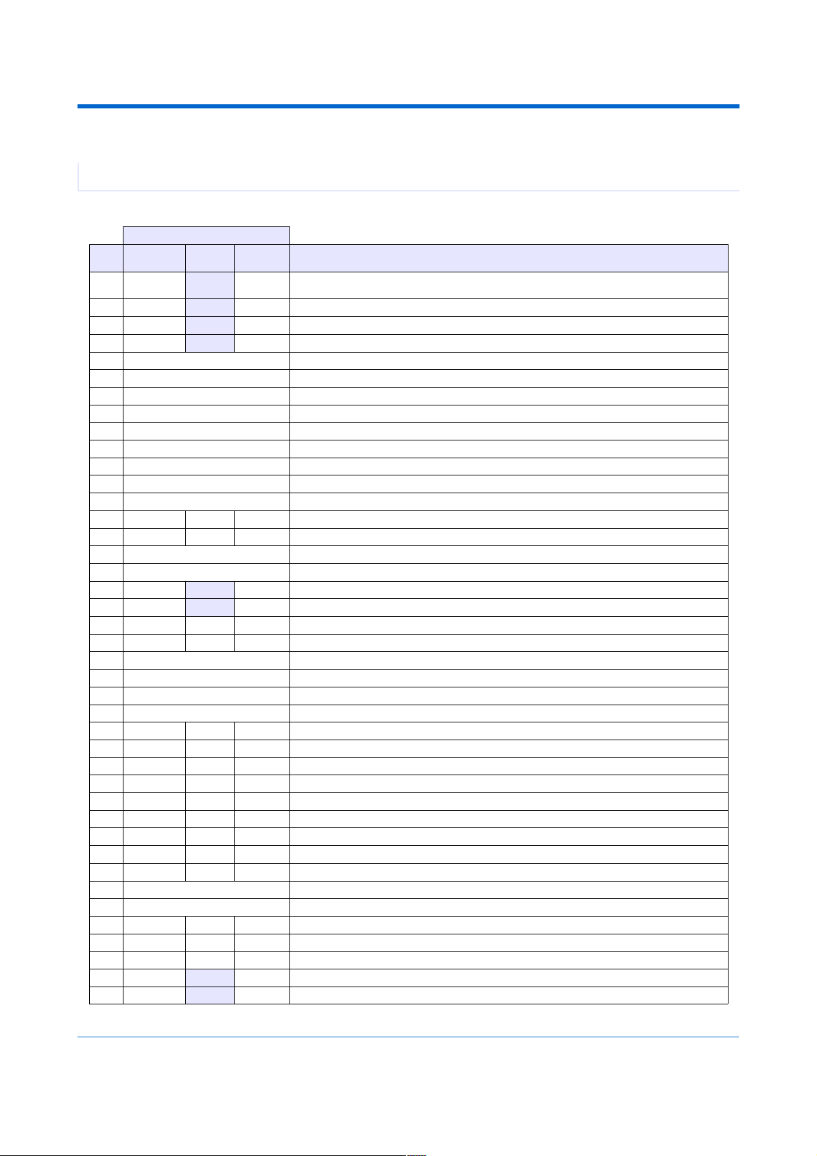
2.2. USBiziTM LQFP 100 Pin-out Table
USBizi LQFP100 chipset is based on LPC2387 from NXP.
Name * Interrupt capable input.
No. LPC2387
H/W
USBizi IO2
nd
Feature
USBizi
Pin Description
6 P0.26 IO22* ADC3/
DAC
ADC3 (10-Bit Analog to Digital Input) or DAC (Digital to Analog Output)
7 P0.25 IO24* ADC2 ADC2 (10-Bit Analog to Digital Input)
8 P0.24 IO26* ADC1 ADC1 (10-Bit Analog to Digital Input)
9 P0.23 IO28* ADC0 ADC0 (10-Bit Analog to Digital Input)
10 VDDA Connect to 3.3 volt source
11 VSSA Connect to Ground
12 VREFA Connect to 3.3 volt source
13 VDD_1 Connect to 3.3 volt source
15 VSS1 Connect to Ground
16 RTCX1 Connect to real-time crystal circuit pin 1
17 RESET# Hardware reset signal, Reset state is on Low
18 RTCX2 Connect to real-time crystal circuit pin 2
19 VBAT Connect to 3.3 volt back up battery to keep the real-time clock running.
20 P1.31 IO32 ADC5 ADC5 (10-Bit Analog to Digital Input)
21 P1.30 IO29 ADC4 ADC4 (10-Bit Analog to Digital Input)
22 XTAL1 Connect to the system's 12MHz. crystal pin1
23 XTAL2 Connect to the systems 12MHz. crystal pin1
24 P0.28 IO31* I2C (open drain pin) I2C Interface SCL
25 P0.27 IO33* I2C (open drain pin) I2C Interface SDA
26 P3.26 IO69 N/A General purpose digital I/O
27 P3.25 IO68 N/A General purpose digital I/O
28 VDD1 Connect to 3.3 volt source
29 USBD+ USB Client Feature USB positive data line, USB (access) debugging interface and for the USB client feature.
30 USBD- USB Client Feature USB negative data line, USB (access) debugging interface and for the USB client feature.
31 VSS2 Connect to Ground
32 P1.18 IO35 PWM1 PWM1 (Pulse Width Modulation Output)
33 P1.19 IO34 N/A General purpose digital I/O
34 P1.20 IO25 PWM2 PWM2 (Pulse Width Modulation Output)
35 P1.21 IO23 PWM3 PWM3 (Pulse Width Modulation Output)
36 P1.22 IO61 N/A General purpose digital I/O
37 P1.23 IO62 N/A General purpose digital I/O
38 P1.24 IO63 N/A General purpose digital I/O
39 P1.25 IO64 N/A General purpose digital I/O
40 P1.26 IO65 N/A General purpose digital I/O
41 VSS3 Connect to Ground
42 VDD_2 Connect to 3.3 volt source
43 P1.27 IO21 N/A General purpose digital I/O
44 P1.28 IO66 N/A General purpose digital I/O
45 P1.29 IO67 N/A General purpose digital I/O
46 P0.0 IO19* CAN1 RD CAN Channel 1 Data Receive pin (In)
47 P0.1 IO15* CAN1 TD CAN Channel 1 Data Transmit pin (Out)
Rev. 4.4 Page 11 of 38 www.ghielectronics.com
GHI Electronics,LLC USBizi User Manual
Pin-Out Description
Name * Interrupt capable input.
No. LPC2387
H/W
USBizi IO2
nd
Feature
USBizi
Pin Description
48 P0.10 IO39* COM3 Serial port (UART) TXD transmit signal (Out) for COM3
49 P0.11 IO38* COM3 Serial port (UART) RXD receive signal (In) for COM3
50 P2.13 IO50* SD_DAT3 SD card 4-bit data bus, data line no. 3
51 P2.12 IO49* SD_DAT2 SD card 4-bit data bus, data line no. 2
52 P2.11 IO48* SD_DAT1 SD card 4-bit data bus, data line no. 1
53 P2.10 IO0* BL# General purpose digital I/O. On power up, this pin is used to access GHI boot loader
when Low (refer to GHI boot loader section)
This pin is high (no loader) if not connected.
54 VDD2 Connect to 3.3 volt source
55 VSS4 Connect to Ground
56 P0.22 IO47* SD_DAT0 SD card 4-bit data bus, data line no. 0
57 P0.21 IO46* MCIPWR Memory card (SD/MMC) power enable signal (refer to the reference design schematic for
connection).
58 P0.20 IO45* SD_CMD SD card 4-bit data bus, command line
59 P0.19 IO44* SD_CLK SD card 4-bit data bus, clock line
60 P0.18 IO41* SPI1 SPI master bus interface MOSI signal (Master Out Slave In) for SPI1
61 P0.17 IO40* SPI1 SPI master bus interface MISO signal (Master In Slave Out) for SPI1
62 P0.15 IO42* SPI1 SPI master bus interface SCK signal (Clock)for SPI1
63 P0.16 IO43* N/A General purpose digital I/O
64 USB_CON USB Client Feature Reports the USB cable attachment to the PC USB Host (refer to the reference design
schematic for the required circuit).
65 P2.8 IO36* N/A Only general purpose digital I/O.
66 P2.7 IO11* COM2 Serial port (UART) RTS signal for COM2
67 P2.6 IO9* N/A General purpose digital I/O
68 P2.5 IO7* PWM6 PWM6 (Pulse Width Modulation Output)
69 P2.4 IO2* PWM5 PWM5 (Pulse Width Modulation Output)
70 P2.3 IO4* PWM4/
MODE
PWM4 (Pulse Width Modulation Output),
On power up, this pin is used to select the communication interface for GHI boot loader
and debugging, between USB (High) or COM1(Low). (refer to GHI boot loader section)
This pin is high (select USB) if not connected.
71 VDD3 Connect to 3.3 volt source
72 VSS5 Connect to Ground
73 P2.2 IO1* COM2 Serial port (UART) CTS signal for COM2
74 P2.1 IO3* COM2 Serial port (UART) RXD receive signal (In) for COM2
75 P2.0 IO5* COM2 Serial port (UART) TXD transmit signal (Out) for COM2
76 P0.9 IO6* SPI2 SPI master bus interface MOSI signal (Master Out Slave In) for SPI2
77 P0.8 IO8* SPI2 SPI master bus interface MISO signal (Master In Slave Out)for SPI2
78 P0.7 IO10* SPI2 SPI master bus interface SCK signal (Clock)for SPI2
79 P0.6 IO12* General purpose digital I/O
80 P0.5 IO14* CAN2 TD CAN Channel 2 Data Transmit pin (Out)
81 P0.4 IO16* CAN2 RD CAN Channel 2 Data Receive pin (In)
82 P4.28 IO13 COM4 Serial port (UART) TXD transmit signal (Out) for COM4
83 VSS7 Connect to Ground
84 VDD_3 Connect to 3.3 volt source
85 P4.29 IO17 COM4 Serial port (UART) RXD receive signal (In) for COM4
86 P1.17 IO60 N/A General purpose digital I/O
87 P1.16 IO59 N/A General purpose digital I/O
88 P1.15 IO58 N/A General purpose digital I/O
89 P1.14 IO57 N/A General purpose digital I/O
Rev. 4.4 Page 12 of 38 www.ghielectronics.com
 Loading...