

Page 1

www.ams.com
Revision 1.0 / 2012/06/26
Application Note: UHF RFID Fermi Reader
HW
AS3993
UHF RFID Single Chip Reader EPC
Class1 Gen2 Compatible
-Description
Page 2

AS3993 – AN13 – Received Signal Str engt h In dicat or (RS SI)
www.ams.com
Revision 2.0 / 6/22/12
page 1/17
7
7
8
5.4 Programming Interface Description........................................................................... 9
10
10
11
6.4 OAD Pins ............................................................................................................... 16
Table of Contents
Introduction .......................................................................................................................... 2
1.
2. Key Features ....................................................................................................................... 3
3. Applications ......................................................................................................................... 4
4. Reader System Description .................................................................................................. 5
5 Interfaces ............................................................................................................................. 7
5.1 USB ..........................................................................................................................
5.2 UART Interface .........................................................................................................
5.3 Pin Header Interface Description ..............................................................................
6 Reader Part ....................................................................................................................... 10
6.1 RF Tracks – Impedance Calculation .......................................................................
6.2 Reader Part – PCB Stackup ...................................................................................
6.3 Reader Part – Schematics ......................................................................................
7 Controller Part .................................................................................................................... 16
Copyright .................................................................................................................................. 17
Disclaimer ................................................................................................................................. 17
Figure 1 - Reader Part ......................................................................................................................... 5
Figure 2 - Controller Part ..................................................................................................................... 6
Figure 3 - Pin Header Position (all dimensions in mm) ....................................................................... 8
Figure 4 - Programming Interface (all dimension s in m m ) .................................................................. 9
Figure 5 - RF Tracks - Impedance Calculation (dimensions in mil) .................................................. 10
Figure 6 - RF Part - PCB Stackup ..................................................................................................... 10
Figure 7 - Schematic Reader Section ............................................................................................... 11
Figure 8 - Schematic Loop Filter ....................................................................................................... 11
Figure 9 - Reader Indicator LEDs ...................................................................................................... 12
Figure 10 - Schematic Balun Section ................................................................................................ 13
Figure 11 - Schematic PA Section .................................................................................................... 14
Figure 12 - Schematic Directional Coupler........................................................................................ 15
Figure 13 - OAD Pads ....................................................................................................................... 16
Figure 14 - Schematic MCU Section ................................................................................................. 16
Page 3

AS3993 – AN13 – Received Signal Str engt h In dicat or (RS SI)
www.ams.com
Revision 2.0 / 6/22/12
page 2/17
1. Introduction
The FERMI Reader is a small form factor and low costs EPC Class 1 Gen 2 UHF RFID
demonstration reader system. Leveraging AS3993 UHF RFID Reader IC, provides close to the
industry’s lowest BOM cost, best in class power consumption with the least amount of
complexity.
Second only to ams FERMI design the low r eader BOM enables UHF RFID markets that have
previously been out of reach due to cost restrain ts. With regards to overall cost vs. performance
the FERMI UHF RFID demo reader is unmatched in the indus try.
With an external PA delivering up to 22 dBm, it is ideally suited for those applications that have
similar cost constraints but require that ex tra power
The FERMI demo reader comes in two parts namely the analogue (reader) and digital
(controller) parts. The user can separate the two stacked boards to fully prove out their own RF
and digital parts. With this se t up it also means the user can eva luate the suitability of RFID in
their current system.
The reader portion is designed such that it can b e easily connected to a host MCU via SPI. The
high level of integration found on the AS3993 UHF RFID Reader IC allows for minimal code
loading and quick implementation.
The designs come with free, fully portable code and all Gerber data and sche matics. This allows
for a quick, trouble free design in.
Page 4

AS3993 – AN13 – Received Signal Str engt h In dicat or (RS SI)
www.ams.com
Revision 2.0 / 6/22/12
page 3/17
2. Key Features
• Interface
o Between the Controller and Host Computer: US B (opt ional U ART)
o Between the Controller and the AS3993 is SPI via a low cost pin header
connection
o Between the RF board and the Antenna we use a U .FL (5 0 O hm) SMA ( Male)
• 5V power suppl y from USB.
• GUI
o Adjust Output Power
o Adjust Receive – Sensitivity
o Adapt to different frequency schemes (FCC ETSI)
o Change Gen2 specific parameters like BLF, Coding , Ant i-Collision Slots, …
o Diagnostic Features: RSSI Measurement, Reflected Power Measure ment
o Support for sending AS3993 related direc t commands
o Advanced Tag Manipulations: R/W to differen t memory b anks, define passwords
o Associate tags with other applications like me dia p layer
o View and easily manipulate register settings with a dvance tool tip te xt.
• Low Power Consu mption: com plete reader s ystem is onl y 780mW (typ), 830mW
(max)
• Fully Gen 2 co mpliant, ISO 18000-6b & 6c
• Differen tial T X chip-output configuration
• Differential RX chip-input configuration
• External p ower a mplifier RF2 172
• Maximum output power 22 dBm scalab le in 2 0 s teps
• Low cost MCU: Microchip (PIC24FJ64GB004)
• Indicator LEDs
Page 5

AS3993 – AN13 – Received Signal Str engt h In dicat or (RS SI)
www.ams.com
Revision 2.0 / 6/22/12
page 4/17
3. Applications
Typical applications for the FERMI demo reader inc lude :
• Embedded Consumer Applications
• Mobile Applicat ions (L ow P ower Handhe ld , PDA’s, Smart P hones)
• Embedded Industrial Applications
• Gaming
• Desk top readers
• Low/Mid powered modules
Page 6
AS3993 – AN13 – Received Signal Str engt h In dicat or (RS SI)
www.ams.com
Revision 2.0 / 6/22/12
page 5/17
1
3
2
5
4
6
7
8
9
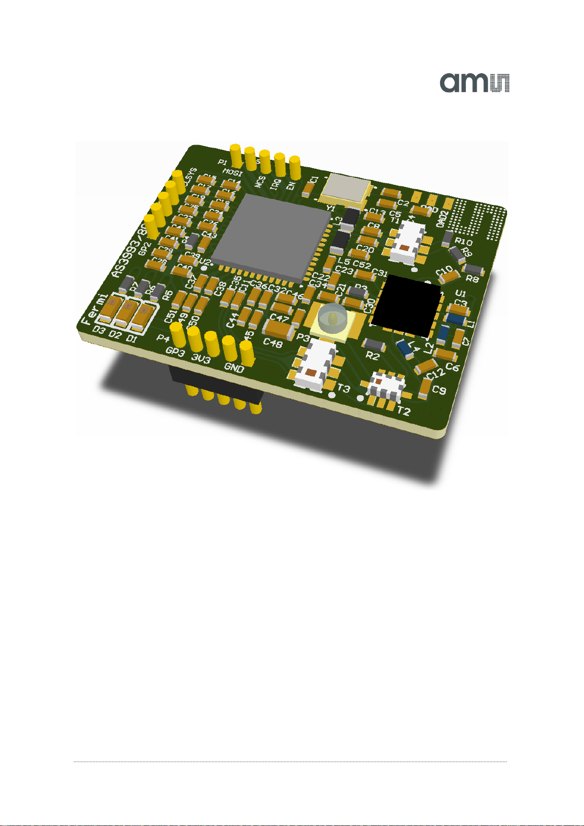
4. Reader System Description
Figure 1 - Reader Part
1. AS3993 UHF RFID reader IC (ams)
2. Balun 2:1 (Johanson Technology)
3. Power Amplifier RF2172 (RFMD)
4. Directional coupler / Low pass filter combination (Joh anson Techn ology)
5. U.FL antenna port (Hirose)
6. Loop Filter
7. OAD pins for debugging purposes
8. Balun 2:1 (Johanson Technology)
9. Crystal 20 MHz +/- 10ppm
Page 7

AS3993 – AN13 – Received Signal Str engt h In dicat or (RS SI)
www.ams.com
Revision 2.0 / 6/22/12
page 6/17
1
3a
2
5
4
6
3c
3b
7
8
Figure 2 - Controller Part
1. MCU C8051F340 (Silabs)
2. USB connector
3. Interface connectors to reader PCB
4. UART connector
5. C2 programming interface for boot loader
6. Indicator LED
7. X-tal (for extended USB functionality)
8. LDO (5 V → 3.5 V)
Page 8

AS3993 – AN13 – Received Signal Str engt h In dicat or (RS SI)
www.ams.com
Revision 2.0 / 6/22/12
page 7/17
TX
GND
RX
5 Interfaces
5.1 USB
The USB is used to communicate to the host computer and to supply the reader system. The 5V
USB voltage is regulated down to 3.5 V.
5.2 UART Inte rface
Page 9

AS3993 – AN13 – Received Signal Str engt h In dicat or (RS SI)
www.ams.com
Revision 2.0 / 6/22/12
page 8/17
EN
IRQ
NCS
MISO
MOSI
CLSYS
CLK
GND
GP1
GP2
GND
GND
3V3
3V3
GP3
In order to establish a connection to the host computer via UART it is recommend to use an USB
TTL serial cable with 3.3 Volt (FTDI TTL-232R-3V3-WE).
5.3 Pin Header Interface Description
Figure 3 - Pin Header Position (all d imensions in mm)
Page 10

AS3993 – AN13 – Received Signal Str engt h In dicat or (RS SI)
www.ams.com
Revision 2.0 / 6/22/12
page 9/17
PGEC
PGED
GND
3V3
MCLR
NC
5.4 Programming Interface Description
Figure 4 - Programming Interface (al l dimensions in mm)
Page 11

AS3993 – AN13 – Received Signal Str engt h In dicat or (RS SI)
www.ams.com
Revision 2.0 / 6/22/12
page 10/17
6 Reader Part
The reader part contains all RF an d UHF RFID relevant comp onents. I n order to keep PCB costs
low the reader part is 2-layer PCB only while all components are located on the top layer. The
component placement was chosen to reach a sm all form factor PCB.
6.1 RF Tracks – Impedance Calcula tion
Figure 5 - RF Tracks - Impedance Calculation ( dimensions in mil)
6.2 Reader Part – PCB Stacku p
Figure 6 - RF Part - PCB Stackup
Page 12

AS3993 – AN13 – Received Signal Str engt h In dicat or (RS SI)
www.ams.com
Revision 2.0 / 6/22/12
page 11/17
6.3 Reader Part – Schematics
Reader Section:
Figure 7 - Schematic Reader Section
Loop Filter:
Figure 8 - Schematic Loop Filter
The loop filter used for the PLL is partly inside the reader IC. The exter nal part is shown above.
The loop filter values are provided by ams. Other values are possible and are mentioned in a
separate application note.
Page 13

AS3993 – AN13 – Received Signal Str engt h In dicat or (RS SI)
www.ams.com
Revision 2.0 / 6/22/12
page 12/17
Indicator LEDs:
Figure 9 - Reader Indicator LEDs
The three indicator LEDs on the reader part together with the LED on the controller part are
used to display error states at the start -up of the reader system. LS B (bit 0) is the controller LED
and reader LEDs D1 – D3 are bit 1 – bit 3. If an error occurs during the start-up the LEDs are
slowly flashing the error code.
Error Codes:
0 : Everything OK. Controller LED flashes fast.
1 : writing + reading SPI fai led.
2 : Reset via EN low + high failed .
3 : IRQ line fail ed.
4 : Crystal not stable (Bit0 in AGC and Internal Status regist er 0x2A)
5 : PLL not locked (Bits1 in AGC and Interna l Status regist er 0x2A)
Example - PLL not locked : Con troller L ED and reader L ED D2 are flashin g slowl y.
Page 14

AS3993 – AN13 – Received Signal Str engt h In dicat or (RS SI)
www.ams.com
Revision 2.0 / 6/22/12
page 13/17
Balun Section:
Figure 10 - Schematic Balun Section
The output impedance of the 0 dBm (low power) outputs are 100 ohm differential. Therefore a
2:1 Balun is used to convert the RF track impedance to 50 ohm singl e ended. In case the ouput
power should be very low the resistor R8, R9 and R 10 (Pi-Pad) can be used to attenuate the RF
signal. It would be also possible to red uce the output power via reader IC register settings but
this should be done only down to -6 dB as the local oscillator signal inside the IC would become
too low. Per default the Pi-Pad is not installed.
Page 15

AS3993 – AN13 – Received Signal Str engt h In dicat or (RS SI)
www.ams.com
Revision 2.0 / 6/22/12
page 14/17
PA Section:
Figure 11 - Schematic PA Section
The PA is supplied by the reader ICs internal voltage regulators. Since the reader ICs internal PA is
not used the corresponding voltage regulator (VDD_PA) is used for the external PA supply. The
power down pin of the external PA is supplied by the VDD_B regulator which is also supplies the 0
dBm output driver of the reader IC. The PA circ ui try matches the proposal of the RF2172 datash eet.
Page 16

AS3993 – AN13 – Received Signal Str engt h In dicat or (RS SI)
www.ams.com
Revision 2.0 / 6/22/12
page 15/17
Directional Coupler and RX Balun Section:
Figure 12 - Schematic Directional Coupler
The directional coupler also includes a low pass filter which attenuates the higher order
harmonics of the carrier signal. The directional coupler is needed in order to prevent the TX
signal leaking into the receiver. The used coupler is a tr ade-off be tween cost and directivity. The
antenna connector is a U.FL connector which is compatible with a microcoaxial connectors.
Since the directional coupler is a 10 dB coupler only 10 dB of the incoming tag signal is fed to
the RX Balun which converts the 50 ohm single ended impedance back to 100 ohm differential
need for the differential RX ports of the reader IC.
Page 17

AS3993 – AN13 – Received Signal Str engt h In dicat or (RS SI)
www.ams.com
Revision 2.0 / 6/22/12
page 16/17
6.4 OAD Pins
The pads J1 and J2 are connected to the OAD pins of the reader IC which c an be used to ou tput
analog/digital RX subcarrier signals or TX / RX based ba nd signals .
Figure 13 - OAD Pads
7 Controller Part
The controller part contains the low cost MCU and the LDO used for reducing t he USB voltage
down to 3.5 Volts. All the interfac es (USB, UART, …) are located on the controller part as well.
In order to allow USB functionality across all to lerances a crystal wi th 12 MHz is a vailable .
Figure 14 - Schematic MCU Section
Page 18

AS3993 – AN13 – Received Signal Str engt h In dicat or (RS SI)
www.ams.com
Revision 2.0 / 6/22/12
page 17/17
Copyright
Copyright © 1997-2012, ams AG, Tobelba der Strasse 30, 8141 Unterpremstaetten, Austria-Europe.
Trademarks Registered ®. All rights r eserved. The material herein may not be reproduced, adapted, merged,
translated, stored, or used without t he pr ior written consent of the copyright owner.
All products and companies mentioned are trademarks or registered trademarks of their respective companies.
Disclaimer
Devices sold by ams AG are covered by the warranty and patent indemnification provisions appearing in its
Term of Sale. ams AG makes no warranty, express, statutory, implied, or by desc ription regarding the
information set forth herein or regarding the freedom of the described devices from patent infringement. ams
AG reserves the right to change specifications and prices at any time and without notice. Therefore, prior to
designing this product into a s ystem , it is necessary to check with ams AG for c ur rent information.
This product is intended for use in norm al c ommercial applications. Applications requiring extended
temperature range, unusual envi r onmental requirements, or high reliability applications, such as military,
medical life-support or lifesustaining equipment are specifically not r ec ommended without additional
processing by ams AG for each application. For shipments of less than 100 parts the manufacturing flow might
show deviations from the standard pr oduction flow, such as test flow or test l oc ation.
The information furnished here by ams AG is believed to be correct and accurate. However, ams AG shall not
be liable to recipient or any third par ty for any damages, including but not li m i ted to personal injury, property
damage, loss of profits, loss of use, i nterruption of business or indirect, spe c i al, incidental or consequential
damages, of any kind, in connection with or arising out of the furnishing, perf or mance or use of the technical
data herein. No obligation or liability to recipient or any third party shall arise or flow out of ams AG rendering of
technical or other services.
Contact Information
Headquarters
ams AG
Tobelbader Strasse 30
8141 Unterpremstaetten
Austria
T. +43 (0) 3136 500 0
For Sales Offices, Distributors and Repr esentatives, please visit:
http://www.ams.com/contact
 Loading...