Gennum Corporation LT505 Datasheet

Low Current, Peak Limiting
Class A Amplifier
LT505 DATA SHEET
FEATURES
• amplifier current typically 53 µA
• transducer current typically 210
µA
• Schottky diodes provide peak limiting
• low parts count
• gain 74dB typically with 1.3 V supply
STANDARD PACKAGING
• 8 Pin PLID
®
• chip ( 56 x 55 mils)
DESCRIPTION
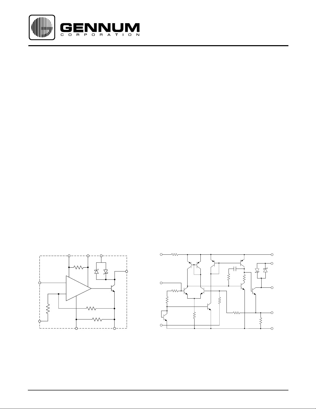
The LT505 is a low current, low voltage monolithic integrated
circuit amplifier. It is comprised of an operational amplifier
driving a single transistor class A output stage with open
collector. Also included is a pair of complementary Schottky
diodes which, when shunted across the load, provide the
capability for symmetrical peak clipping.
The input stage is biased by an external 200 kΩ resistor. It is
important that this resistor be ±1% tolerance for optimum
performance. An internal negative feedback loop ensures a
stable operating point for the output stage over the designed
operating voltage. Because of the lowered idle current,
trimming the output current with the use of a single external
resistor is not recommended for the LT505.
The typical gain for this IC is 74 dB. Due to low power consumption
this part is the perfect choice for the output
stage of class A hearing instruments.
BLOCK DIAGRAM
V
MIC
8
6
I/P
+
_
100
5
R
VC
GND
All resistors in ohms, all capacitors in µF unless otherwise stated U.S. Patent No. 4,034,306 Patented in other countries
Revision Date: January 2001
2.2K
EQUIVALENT CIRCUIT
V
MPO
B
1
4
O/P
3
33K
200
7
2
R
E
2.2 K
8
6
27 K
5
100
33 K
Document No. 500 - 45 - 10
4
1
3
2
200
7
GENNUM CORPORATION P.O. Box 489, Stn. A, Burlington, Ontario, Canada L7R 3Y3 tel. +1 (905) 632-2996
Web Site: www.gennum.com E-mail: hipinfo@gennum.com

ABSOLUTE MAXIMUM RATINGS
PIN CONNECTION
PARAMETER VALUE/UNITS
5
Supply Voltage 3 V DC
Power Dissipation 25 mW
Operating Temperature Range -10°C to 40° C
O / P
MPO
4
V
B
R
E
1
R
VC
I / P
GND
8
V
MIC
CAUTION
CLASS 1 ESD SENSITIVITY
ELECTRICAL CHARACTERISTICS
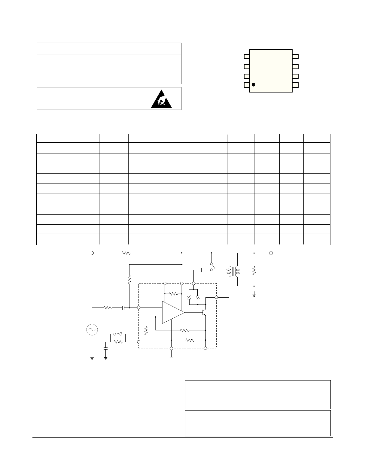
All switches remain as shown in test circuit unless stated in conditions column. Conditions : V
PARAMETER SYMBOL CONDITIONS MIN TYP MAX UNITS
Gain V
Total Harmonic Dist. V
Amplifier Current I
Transducer Current I
Total Current IA+ I
A
L
L
= 200 mV
OUT
= 200 mV
OUT
RMS
RMS
Input Referred Noise
Volume Control Range RVC = 0 to 56.2 kΩ (S1 -ON/OFF)
Battery Resist.Stability RB= 22 Ω
Input Impedance (Pin 6)
Maximum Output V
= 0.5 m V
I
N
(S2 - closed)
RMS
= 1.30 VDC , temperature 25˚ C
CC
70
-
44
130
174
-
36
22
-
0.165
74
2.0
53
210
263
1.4
47
-
15
0.240
78
5.0
62
260
322
2.2
-
-
-
0.310
µV
V
dB
%
µA
µA
µA
RMS
dB
Ω
kΩ
RMS
VB = 1.3 VDC
RS = 3.9 K
RB = 4.7
200 k
0.33
V
1.1
S2
+
2.2
4
8
2.2 K
6
1
3
HAMMOND
99966
O
6 K
+
_
33 K
200
7
2
DOCUMENT IDENTIFICATION: DATA SHEET
The product is in production. Gennum reserves the right to make
changes at any time to improve reliability, function or design, in
order to provide the best product possible.
REVISION NOTES:
Changes to standard packaging information.
© Copyright April 1982 Gennum Corporation. All rights reserved. Printed in Canada.
2
+
RVC = 56.2 K
S1
100
5
1 kHz
50Ω
10
All external resistors in ohms, all capacitors in µF unless otherwise stated
Fig. 1 Test Circuit
GENNUM CORPORATION
MAILING ADDRESS:
P.O. Box 489, Stn. A, Burlington, Ontario, Canada L7R 3Y3
Tel. +1 (905) 632-2996 Fax +1 (905) 632-2814
SHIPPING ADDRESS:
970 Fraser Drive, Burlington, Ontario, Canada L7L 5P5
GENNUM JAPAN CORPORATION
C-101, Miyamae Village, 2-10-42 Miyamae, Suginami-ku, Tokyo 168-0081,
Japan Tel. +81 (3) 3334-7700 Fax: +81 (3) 3247-8839
Gennum Corporation assumes no responsibility for the use of any circuits described herein and makes no representations that they are free from patent infringement.
500 - 45 -10
 Loading...