Gennum Corporation LS505 Datasheet

High Gain Class A Amplifier
with Peak Clipping
LS505 DATA SHEET
FEATURES
• 72 dB typical gain
• 0.2 to 2.0 mA of transducer current adjustment
• 43 dB range of feedback volume control
• 1.0 to 1.6 V supply operating range
• Schottky diodes provide symmetrical peak clipping
• requires only 4 external parts for operation
STANDARD PACKAGING
• 8 pin MINIpac
• 8 pin MICROpac
• 8 pin PLID
®
• 8 pin SLT
• Chip (56 x 55 mils)
DESCRIPTION
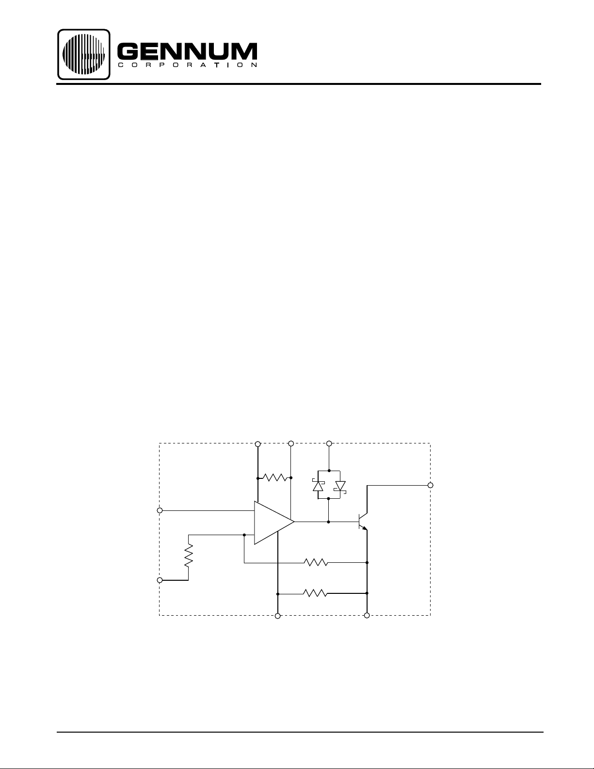
The LS505 is a low voltage, monolithic integrated circuit
amplifier comprised of an operational amplifier driving a
single transistor Class A output stage with open collector.
Also included are a pair of complementary Schottky diodes
which provide the capability for symmetrical peak clipping in
a feedback configuration.
An internal negative feedback loop ensures a stable operating
point for the output stage over the designed operating voltage.
This also permits trimming of the output current with the use
of a single external resistor.
The input stage and microphone are biased by an internal
2.2 kΩ decoupling resistor to increase battery line signal
rejection.
V
MIC
8 1
I/P
6
100
R
VC
5
+
-
BLOCK DIAGRAM
All resistors in ohms, all capacitors in farads unless otherwise stated.
2.2k
GND
VB
4
7
33k
200
MPO
RE
O/P
3
2
Revision Date: January 1996
GENNUM CORPORATION P.O. Box 489, Stn A, Burlington, Ontario, Canada L7R 3Y3 tel. (905) 632-2996 fax: (905) 632-5946
Japan Branch: A-302, Miyamae Vi llage, 2–10–42 Miyamae, Suginami–ku Tokyo 168, Japan tel. (03) 3334-7700 fax (03) 3247-8839
Document No. 500 - 20 - 11

ABSOLUTE MAXIMUM RATINGS
PIN CONNECTION
PARAMETER VALUE & UNITS
Supply Voltage 3 V
Power dissipation 25 mW
Operating Temperature -10 to +40 °C
O/P
MPO
V
4
B
R
E
1
R
5
VC
I/P
GND
V
8
MIC
Storage Temperature -20 to +70 °C
CAUTION
CLASS 1 ESD SENSITIVITY
ELECTRICAL CHARACTERISTICS
Conditions: Temperature 25 oC, Supply Voltage VB = 1.55 VDC
PARAMETER SYMBOL CONDITION MIN TYP MAX UNITS
Gain A
Temperature Coefficient of Gain η
Amplifier Current I
Temperature Coefficient of Current η
Transducer Current I
CL
A
AMP
Ι
TRANS
Total Harmonic Distortion THD VO = 0.707 VRMS -25 %
VO = 0.707 VRMS 68 72 76 dB
- 0.07 - dB/oC
180 210 280 µA
- -0.002 - mA/oC
1.3 1.5 1.9 mA
Input Referred Noise IRN NFB 0.2 to 10 kHz at 12 dB/oct - 1.2 2.0 µVRMS
Battery Resistance Stability RB = 22Ω --22 Ω
Volume Control Range RVC = 100 to 100.1 kΩ S1 open 36 43 - dB
Input Impedance (Pin 6) R
IN
-27- kΩ
Frequency Response (-3 dB) Low - 100 - Hz
High - 5K - Hz
Maximum Output S2 closed 0.125 0.19 0.275 VRMS
Gain Dependence of RB - 0.16 - dB/Ω
Emitter Bias Voltage (Pin 2) V
All switches and parameters remain as shown in test circuit unless stated in condition column
500 - 20 - 11
RE
2
- 42.5 - mV
 Loading...