Gennum Corporation LP508 Datasheet

Class A Amplifier with
2 Independent Gain Blocks
LP508 DATA SHEET
FEATURES
• 1 µV input referred noise
• 1.0 to 5 VDC operating range
• 61 dB typical gain (adjustable)
• 0.28 to 2.0 mA range of transducer current
• 1 % electrical distortion
• the first and second blocks can be DC coupled
Ω microphone decoupling resistor, on-chip
• 4.0 k
• 100 Hz to 50 kHz frequency response
• volume control range >40 dB
STANDARD PACKAGING
• 8 pin MICROpac
• 8 pin PLID
®
• 8 pin SLT
• Chip (59 x 53 mils)
Au Bump
DESCRIPTION
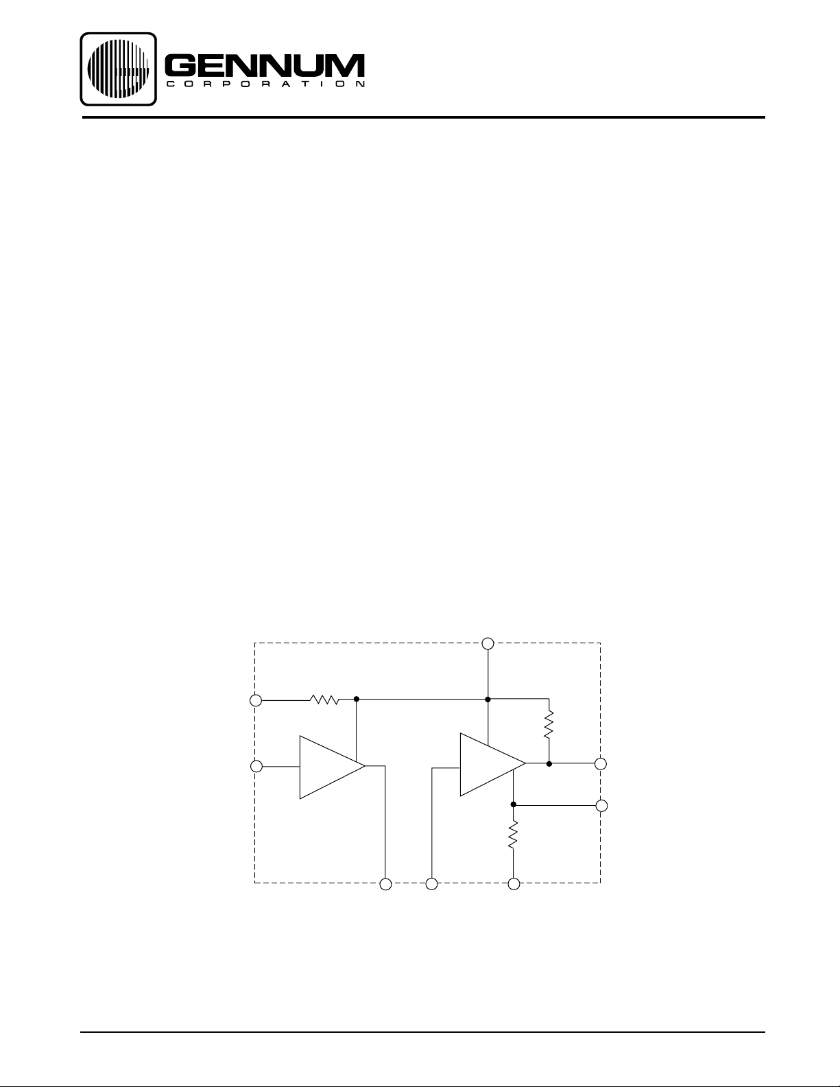
The LP508 is an 8 pin Class A amplifier utilizing Gennum's
proprietary low voltage bipolar JFET technology. It consists of
2 single ended, low noise inverting gain blocks. The first block
has a typical open loop gain of 50 dB, with the closed loop gain
set by the ratio of the feedback resistor to the the source
impedance. The second block has the output transistor bias
R
and
V
set by
E
at pin 7 which is 27 mV.
RE
Typically, the gain of the first block is set to 29 dB, with the
second block at 32 dB, giving a total gain of 61 dB.
Revision Date: January 2001
V
MIC
A IN
V
B
5
R
4
MIC
18K
3
-
A
A OUT
1
B IN
-
B
R
E
8
2
GND
6
B OUT
7
R
E
BLOCK DIAGRAM
Document No. 500 - 71 - 9
GENNUM CORPORATION P.O. Box 489, Stn. A, Burlington, Ontario, Canada L7R 3Y3 tel. +1 (905) 632-2996
Web Site: www.gennum.com E-mail: hipinfo@gennum.com

ABSOLUTE MAXIMUM RATINGS
PIN CONNECTION
PARAMETER VALUE/UNITS
Supply Voltage 5 V DC
Power Dissipation 25 mW
Operating Temperature Range -10°C to 40° C
Storage Temperature Range -20°C to 70° C
V
MIC
A IN
GND
A OUT
4
1
5
V
B
B OUT
R
E
B IN
8
CAUTION
CLASS 1 ESD SENSITIVITY
ELECTRICAL CHARACTERISTICS
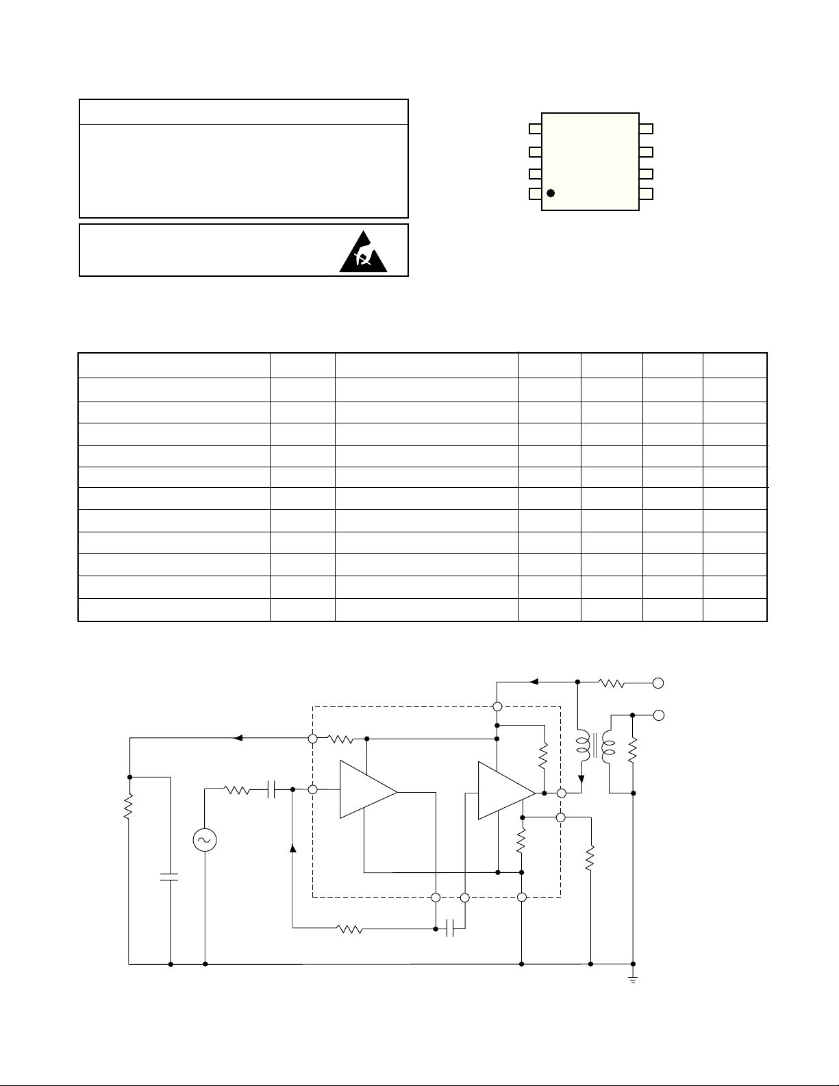
Conditions: Frequency = 1 kHz, Temperature = 25°C, Supply Voltage VB = 1.3 VDC
PARAMETER SYMBOL CONDITIONS MIN TYP MAX UNITS
Gain (Closed Loop) A
CL
Distortion THD V
Amplifier Current I
Transducer Current I
Transducer Current I
AMP
TRANS H
TRANS L
Input Referred Noise IRN NFB 0.2 to 10 kHz at 12 dB/oct. - 1 2 µV
Stable with Battery Resistance to - - 22 Ω
Input Bias Current (pin 3) I
On Chip Emitter Resistor R
Emitter Bias Voltage (Pin 7) V
Microphone Decoupling Resistor R
All parameters and switches remain as shown in Test Circuit unless otherwise stated in "Conditions" column
B
E
RE
MIC
V
=500mVRMS 57 61 65 dB
OUT
=500mVRMS - 1 4 %
OUT
I
= I
+
AMP
I
A
MIC
125 195 255 µA
RE = 27.5 1.1 1.3 1.7 mA
RE = ∞ 200 275 350 µA
-50 0 50 nA
- 100 - Ω
-27-mV
-4-kΩ
500 - 71 - 9
R
I
MIC
R
S
3.3K
33K
V
IN
1kHz
C2
10
All resistors in ohms, all capacitors in µF unless otherwise stated
C1
10
I
B
MIC
4
- A
3
R
=100K
FA
1
8
C3
1.0
Fig. 1 Test Circuit
2
5
- B
RB= 4.75
R
E
=27.5
VB=1.3 VDC
V
OUT
R
L=1K
I
AMP
18K
6
I
TRANS
7
R
E
2
 Loading...