Dual, Continuous, Analog
Highpass Filter
LF580 DATA SHEET
FEATURES
• only 2 small capacitors required
• 200 to 10 kHz adjustable corner frequency
• dual 12 dB/Oct Butterworth filter (24 dB/Oct cascaded)
• 1.1 to 3.0 VDC operating range
• adjustable by a single potentiometer
STANDARD PACKAGING
• 8 pin MICROpac
• 8 pin PLID
®
• Chip (66 x 61mils)
DESCRIPTION
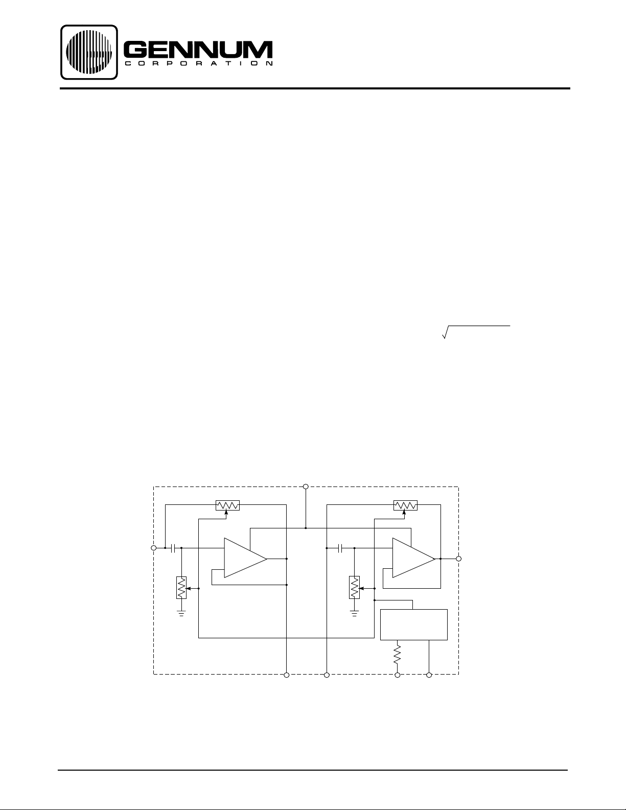
The LF580 continuous analog filter consists of two second
order (12 dB/oct), tunable (0.2 to 10 kHz) highpass Butterworth
filter blocks.
Tracking and corner frequency of each block are controlled
by a single potentiometer. Cascading the two blocks
together results in a single 24dB/oct high pass filter requiring
only two external 0.001 µF capacitors for the filter response.
The output noise of each filter stage is typically 5.6µV.
Cascading the two filter blocks together will produce a
noise level which is
V
= (VN1)2 + (VN2)
N
2
Where VN is the total output noise of both filters, VN1 and
V
is the noise of each filter.
N2
To improve the signal-to-noise ratio of the filter the LF580
should be placed after a preamplifier, provided that the
signal level does not exceed the maximum signal capability
of 50mV
RMS
A
IN
Revision Date: January 2001
V
B
4
8
0.001
All resistors in ohms, all capacitors in microfarads unless otherwise stated
+
AB
_
7
A
OUT
0.001
631
B
IN
BLOCK DIAGRAM
1.8k
+
_
CONTROL
GNDCONTROL
5
B
OUT
Document No. 500 - 73 - 08
GENNUM CORPORATION P.O. Box 489, Stn. A, Burlington, Ontario, Canada L7R 3Y3 tel. +1 (905) 632-2996
Web Site: www.gennum.com E-mail: hipinfo@gennum.com

ABSOLUTE MAXIMUM RATINGS
PIN CONNECTION
PARAMETER VALUE/UNITS
Supply Voltage 5 V DC
Operating Temperature Range -10°C to 50° C
Storage Temperature Range -40°C to 100° C
V
CONTROL
N/C
GND
B
TOP VIEW
4
1
5
8
CAUTION
CLASS 1 ESD SENSITIVITY
ELECTRICAL CHARACTERISTICS
Conditions: Frequency = 1 kHz, Temperature = 25°C, Supply Voltage VB = 1.3 V
Parameter Symbol Conditions Min Typ Max Units
Insertion Loss V
Current Drain I
Corner Frequency f
T
C
Distortion THD V
R
V
IN
CNT
IN
IN
=1 V
=1 V
=1.25 V
Note 1 - 2 3 dB
RMS
= 100 kΩ 200 280 370 µA
Note 2 1300 1650 1900 Hz
RMS
RMS
- 2 5 %
Ouput Noise Note 3 - 8 10 µV
Supply Rejection SR VB = 3.0VDC Note 4 - 45 56 dB
B
B
A
A
OUT
IN
OUT
IN
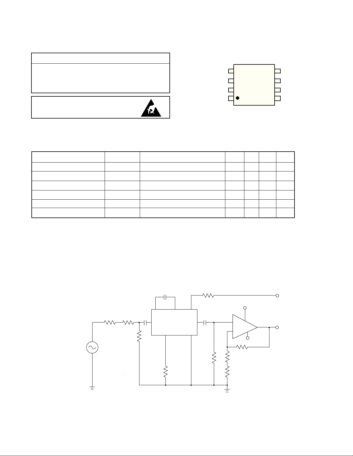
All parameters and switches remain as shown in Test Circuit unless otherwise stated in "Conditions" column
Notes 1: Insertion Loss = 20 Log(V
2: a) measure output voltage V
b) measure output voltage V
= 1000 x 2
f
C
3: Output Noise = V
modulated with 1V
4: V
Supply Rejection = 20 Log (V
B
(V
V
/
OUT1
OUT2
/100, filter bandwidth 200Hz to 10kHz at 12dB/Oct
OUT
RMS
V
IN
)-12
OUT/VIN
OUT1 (RCNT
OUT2 (RCNT
)
at 1 kHz
)-40
OUT
ATTENUATOR
28dB
=100kΩ)
=10.274kΩ)
0.0011501.82k
82.1
0.001
764
LF580
8
5
31
RL=10k 1000
=100k
R
CNT
R
1.0
B
=4.7
10
+
IC1
40.0 dB
_
100k
+15 V
-15 V
VB=1.3 VDC
DC
DC
V
OUT
500 - 73 - 08
All resistors in ohms, all capacitors in microfarads unless otherwise stated in conditions column
Fig. 1 Test Circuit
2
 Loading...