Gennum Corporation LE507 Datasheet

Class A Output Stage
with Input Biasing
LE507 DATA SHEET
FEATURES
• 76 dB of gain
• internal DC bias for I/P stage
• applications include AF output stages,
hearing aids and RF amplifiers
• total harmonic distortion 1% (typical)
STANDARD PACKAGING
• 8 pin PLID ®
• 8 pin DIP
V
BIAS
V
B
DESCRIPTION
The LE507 is a low voltage class A amplifier design, primarily
for low voltage and low power use. The broad application
include AF output stages, RF amplifiers and output stages of
the hearing instruments. The circuit is comprised of three
stages all of them having access to their collectors for
frequency shaping, feedback, etc. The provision for the bias
network and alternative gain increase to 76 dB are included on
the circuit.
For ␣ more application information refer to Information Note
520 - 30.
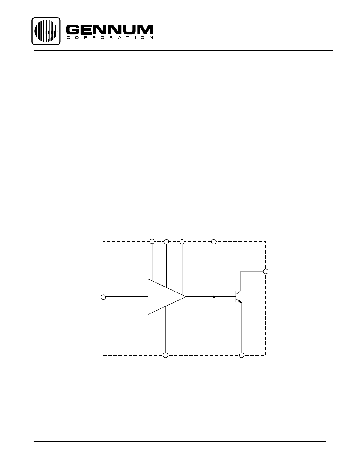
FILTER A
FILTER B
1
(2)
4
(1)
3
2
(3)
(4)
I/P
5
(8)
GND
All external resistors in ohms, all capacitors in µF unless otherwise stated.
Numbers in brackets are for DIP package.
BLOCK DIAGRAM
(5)
8
O/P
7
(6)
6
(7)
R
E
Revision Date: January 2001
GENNUM CORPORATION P.O. Box 489, Stn A, Burlington, Ontario, Canada L7R 3Y3 tel. (905) 632-2996 fax: (905) 632-5946
Japan Branch: A-302, Mi yamae Vil lage, 2–10–42 Mi yamae, Suginami–ku, Tokyo 168, Japan tel. (03) 3334-7700 fax (03) 3247-8839
Document No. 500 - 52 - 09

ABSOLUTE MAXIMUM RATINGS
PIN CONNECTION
PARAMETER VALUE/UNITS
Supply Voltage 5 V DC
Power Dissipation 25 mW
Operating Temperature Range -10°C to40° C
Storage Temperature Range -20°C to 70° C
CAUTION
CLASS 1 ESD SENSITIVITY
ELECTRICAL CHARACTERISTICS
FILTER A
GND
V
BIAS
FILTER A
GND
V
BIAS
4
V
1
B
1
DIP
PACKAGE
4
V
B
5
I / P
R
E
O / P
FILTER B
8
8
I / P
R
E
O / P
FILTER B
5
Supply voltage 1.3 VDC, ambient temperature 25oC
Conditions are as per test circuit unless otherwise stated
PARAMETER SYMBOL CONDITIONS MIN TYP MAX UNITS
Voltage Gain V
A
Output level 0.5 VRMS 28 30 32 dB
Total Harmonic Distortion T.H.D. Output level 0.5 VRMS -12%
Total Current I
Emitter Voltage V
Total
RE
1.05 1.3 1.6 mA
27 34 41 mV
INPUT
R
S
ATTENUATION
100 k
600
1 kHz
-30 dB
3.3 k
680
33 k
0.033
4
(1)
25 k
2
(3)
2 k
5
(8)
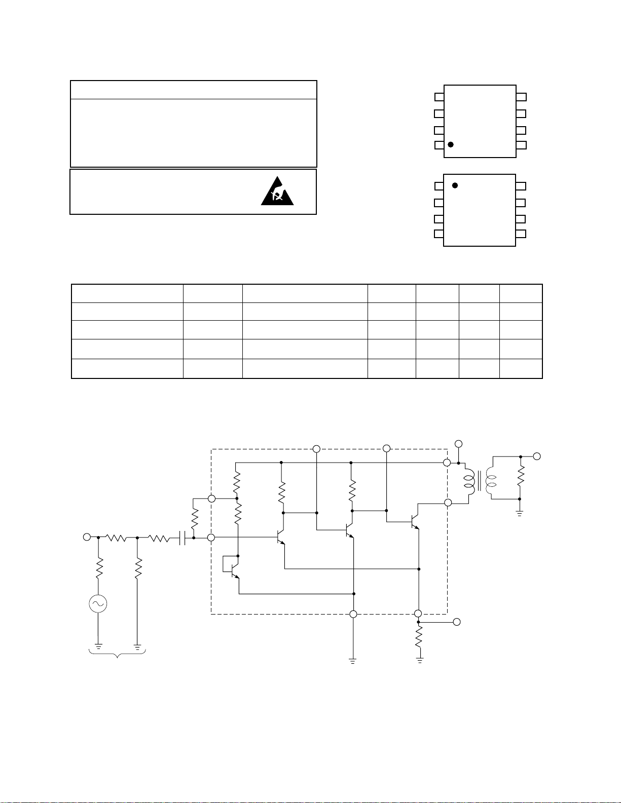
All external resistors in ohms, all capacitors in µF unless otherwise stated.
Numbers in brackets are for DIP packages.
18 k
13.5 k
3
(2)
8
(5)
Fig.1 Test Circuit
VB = 1.3 VDC
I
TOT
1:1
HAMMOND
99966
V
RE
1
(4)
7
(6)
6
(7)
27
V
R
1 k
OUT
L
500 - 52 - 09
2
 Loading...