Low Parts
Compression Amplifier
GB512/LD512 DATA SHEET
FEATURES
• 44 dB typical preamplifier gain
• 14 dB typical output stage gain
• compression function ratio 1:1 to 2:1 to
• automatic setting of transducer current
• operation down to 1.1 VDC
• greater than 40 dB volume control range
STANDARD PACKAGING
• 8 pin PLID
• 8 pin SLT (LD512)
• Chip (61 x 61 mils)
Au Bump
∞:1
DESCRIPTION
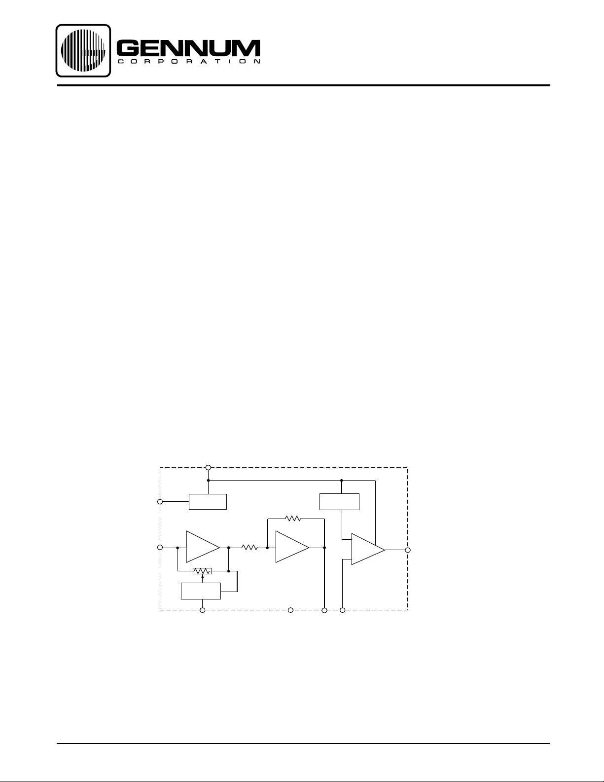
The GB512 and LD512 are 8 pin stand-alone input compression
amplifiers requiring minimal external parts. Each consists of a
voltage regulator for the electret microphone providing a high
power supply rejection ratio (PSRR), a compression stage
which has a 2:1 compression ratio, and an auto-biasing,
class A, voltage drive output stage.
The auto-bias output stage can drive a variety of impedances
ranging from 500 Ω to 5 kΩ without adding any external
resistors to set the bias.
The GB512 and LD512 are recommended for low to medium
gain/output ITE and ITC type hearing aids.
The GB512 is tested to tighter test limits.
V
REG
A IN
Revision Date: January 2001
4
3
V
V
REG
28 dB
A
-
CONTROL
2
C
AGC
B
5
200 mV
REF
16 dB
-
B
6
GND B OUT C IN
+
C
_
1
8
7
C OUT
BLOCK DIAGRAM
Document No. 500 - 75 - 08
GENNUM CORPORATION P.O. Box 489, Stn A, Burlington, Ontario, Canada L7R 3Y3 tel. (905) 632-2996 fax: (905) 632-5946
Japan Branch: A-302, Miyamae Village, 2-10-42, Miyamae, Suginami-ku, Tokyo 168, Japan tel. (03) 3334-7700 fax (03) 3247-8839

ABSOLUTE MAXIMUM RATINGS
PIN CONNECTION
PARAMETER VALUE/UNITS
5
Supply Voltage 5 V DC
Power Dissipation 25mW
Operating Temperature Range -10°C to 40°C
Storage Temperature Range -20˚C to 70˚C
V
REG
A IN
C
AGC
B OUT
4
1
V
B
GND
C OUT
C IN
8
CAUTION
CLASS 1 ESD SENSITIVITY
ELECTRICAL CHARACTERISTICS
Conditions : Temperature 25˚C, Frequency 1 kHz, Supply Voltage 1.3 VDC.
PARAMETER SYMBOL CONDITIONS MIN TYP MAX MIN TYP MAX UNITS
Amplifier Current I
Regulator Voltage V
Output Level V
Output Level V
Output Level V
Output Level V
AMP
REG
O1
O2
O3
O4
VIN = -88 dBV
VIN = -74 dBV
VIN = -54 dBV
VIN = -40 dBV
110
0.88
VO1 + 7
VO2 + 8
Input Referred Noise IRN NFB 0.2-10kHz at 12dB/oct
Total Harmonic Distortion THD VIN = -54 dBV
Receiver Bias Voltage V
Current Sinking Capability I
Release Time Factor T
Attack Time Factor T
All parameters and switches remain as shown in the Test Circuit unless stated in CONDITIONS column.
- actual voltage measured on the pin at given condition (X is pin number).
V
PX
BIAS
SINK
REL
ATT
Note 3
Note 4
100
GB512 LD512
290
0.98
-41
VO1 + 11
VO2+12
-18
3
4
300
-
-
-
110
0.88
-48
-
VO2 + 7
-23.5
-
-
160
3
-
-
-47
-23
200
0.93
-44
VO1 + 9
VO2+10
-20
-
-
1
2
200
3
-
-
8
100
5
200
0.93
-44
-
VO2+10
-20
1
2
200
8
100
5
290
0.98
-40
-
VO2+13
-17.5
3
4
240
-
-
-
µA
V
dBV
dB
dB
dBV
µV
%
mVDC
mA
ms/µF
ms/µF
DC
RMS
VO4
V
O/P
V
LEVEL
(dBV)
at PIN 1
V
500 - 75 - 08
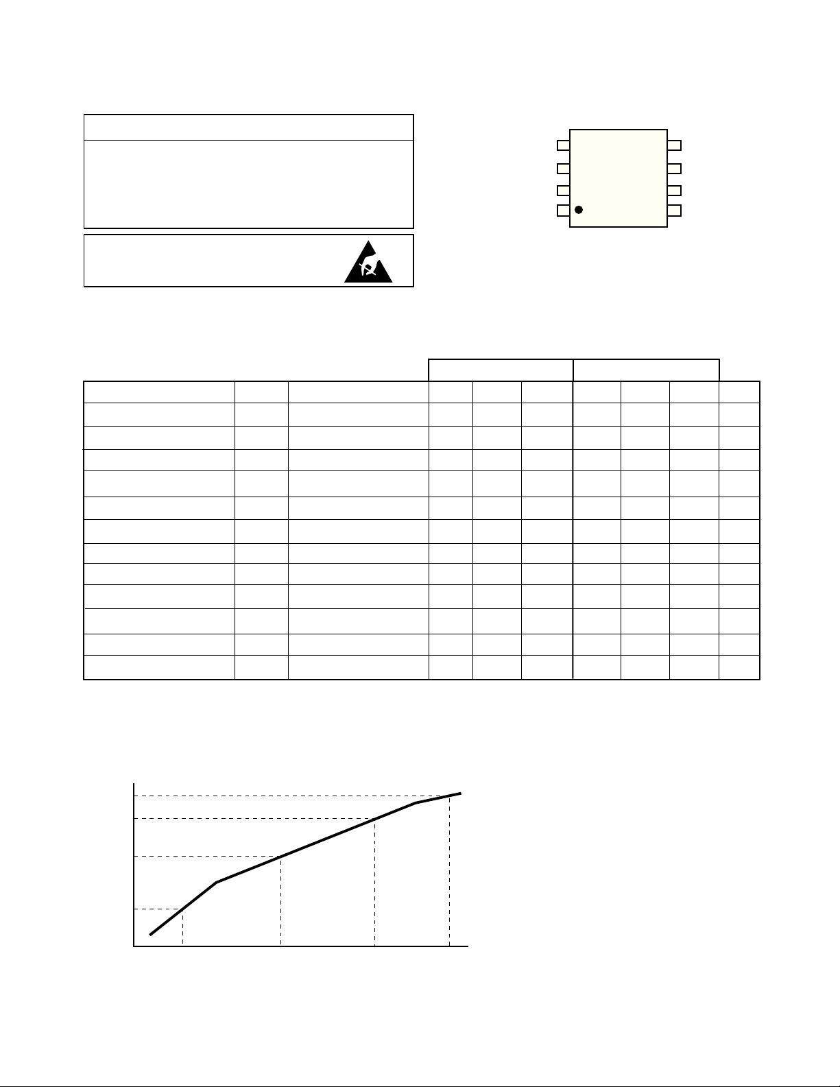
Notes: 1. VO and Distortion measurements are taken
3
O
2
O
1
O
-88 dBV
-74 dBV
IN
IN
-54 dBV
-40 dBV
IN
IN
at pin 1.
2. Output stage gain = 20 log (R
A gain of 14 dB is recommended for
optimal stability. Stability is dependent
upon the ratio of the receiver impedance
) and the battery impedance to RF & RS.
(Z
L
/ RS) < (ZL/ RB)
(R
F
= VP5 - V
3. V
BIAS
4. Measured at pin 7
P7
/ RS).
F
2
 Loading...