Gennum Corporation LC551 Datasheet

High Power
Class B Output Stage
LC551 DATA SHEET
FEATURES
• adjustable gain to 48 dB
• capable of driving low impedance receiver (110
• low parts count, 3 small capacitors & 1 resistor
• gain trim can be used as volume control for
reduced noise
• minimal start - up transient
• frequency bandwidth of 18 kHz
STANDARD PACKAGING
• 10 pin PLID
• Chip (80 x 61 mils)
®
Ω)
DESCRIPTION
The LC551 is a 10 pin low voltage, class B amplifier which
operates over a battery voltage range of 1.1 V DC to 3 V DC.
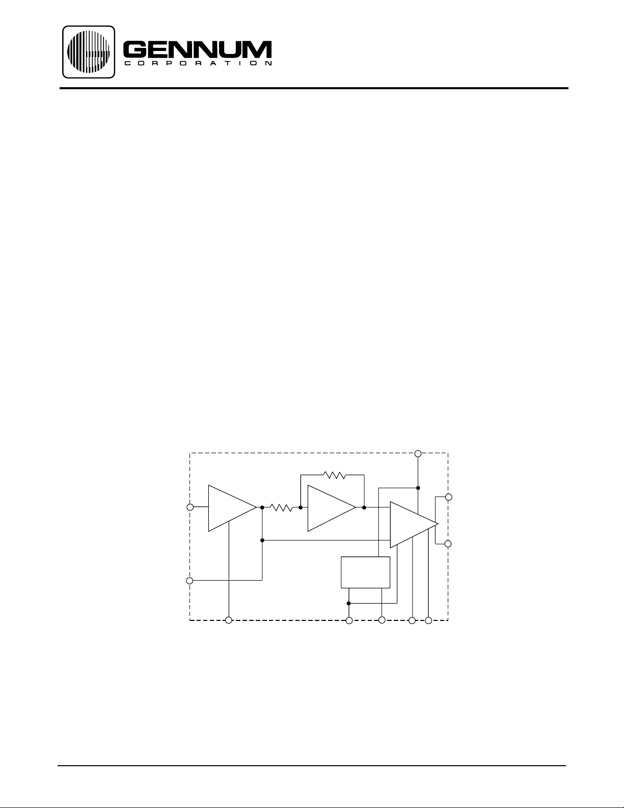
The LC551 consists of three gain blocks. The first block is an
inverting amplifier with the gain set by two external resistors.
This gain trim feature can be used as a volume control in
hearing aid applications. The second block is an inverting
unity gain amplifier which serves as a phase splitter. The
outputs from the first and second blocks drive the differential
inputs of the third block. The third block has a fixed
of 28 dB when driving a receiver.
This amplifier has internal compensation eliminating the need
for a capacitor across the receiver. Two ground pins are
available for "
distortion produced by ground line resistance.
star
" grounding to reduce any second harmonic
V
B
6
AC gain
10
5
A
IN
- A
- B
C
NOT RECOMMENDED
REFERENCE
VOLTAGE
A
OUT
4
O/P2
O/P1
1
FOR NEW DESIGNS
Revision Date: January 2001
GENNUM CORPORATION P.O. Box 489, Stn. A, Burlington, Ontario, Canada L7R 3Y3 tel. +1 (905) 632-2996
2
GND 1
U.S. Patent No. 4,719,430, other patents pending.
BLOCK DIAGRAM
Web Site: www.gennum.com E-mail: hipinfo@gennum.com
9
GND 2
7
REF DEC2 DEC1
8
3
Document No. 500 - 77 - 5

ABSOLUTE MAXIMUM RATINGS
PIN CONNECTION
PARAMETER VALUE/UNITS
Supply Voltage 5 V
Operating Temperature Range -10° C to 40° C
Storage Temperature Range -20° C to 70° C
CAUTION
A
A
OUT
DEC1
GND1
O/P1
IN
TOP VIEW
5
1
V
6
10
B
V
REF
DEC2
GND2
O/P2
CLASS 1 ESD SENSITIVITY
ELECTRICAL CHARACTERISTICS
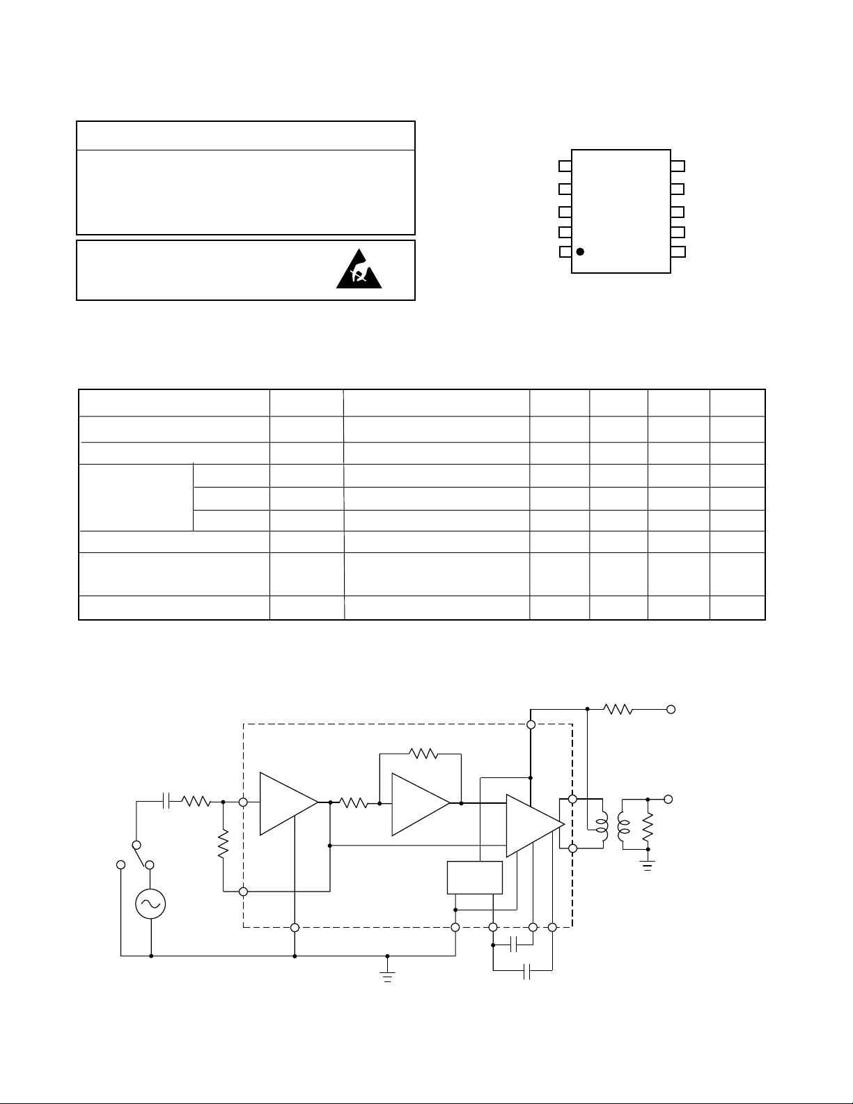
All switches remain as shown in Test Circuit unless stated in condition column
Conditions: Supply voltage V
PARAMETER SYMBOL CONDITIONS MIN TYP MAX UNITS
Gain A
Gain Expansion Ouput Level 1.3 VRMS - -3dB
Quiescent Current: Amplifier I
Transducer I
Total I
Input Referred Noise VIN = 0 (S1 - A) - 1.3 2.5 µV
Total Harmonic Distortion THD Output Level 1.3 VRMS - 3 5.2 %
Stable with battery resistance to - 22 - Ω
= 1.3 V DC, Temperature ambient = 25°C, Noise Filter Bandwidth at 12 dB/Oct (0.2 to 10 kHz)
B
V
AMP
TR
TOT
46 48 50 dB
120 210 335 µA
120 220 405 µA
240 430 740
Output Level 0.707 VRMS - 1.2 2.5 %
500 - 77 - 5
NOTES: 1. Gain expansion = Gain (at 1.3 VRMS output) - Gain (at 0.707 VRMS output)
2. Output impedance is typically 8 Ω with V
0.1
R
+
S1
a
All resistors in ohms, all capacitors in µF unless otherwise stated
S
10K
R
VC
100K
b
V
IN
1kHz
5
- A
4
GROUND 1
2
= 0.5 VRMS
OUT
- B
REFERENCE
9
GROUND 2
Fig. 1 Test Circuit
2
VOLTAGE
7
0.047
6
C
8
0.047
3
10
1
RB = 4.7
HAMMOND
99966
V
B
V
o
RL = 400
Ω
 Loading...