Gennum Corporation LC508 Datasheet

- A
B IN
R
C OUT
V
E
B
GND
A OUT
A IN
V
MIC
1
2
4
3
R
MIC
8
7
5
6
- B
- C
10
9
B OUT
C IN
R
E
LC508 DATA SHEET
BLOCK DIAGRAM
Class A Amplifier with 3
Independent Gain Blocks
FEATURES
• 1
µV input referred noise
• 1.0 to 5 VDC operating range
• 73 dB typical gain (adjustable)
• 0.28 to 2.0 mA range of transducer current
• 1% electrical distortion
• the first and second blocks, or second and third
blocks can be DC coupled
• 100 Hz to 50 kHz frequency response
• suitable for active filtering
STANDARD PACKAGING
• 10 PIN MICROpac
•10 pin PLID
®
• 10 pin SLT
• Chip (52 x 49 mils)
DESCRIPTION
The LC508 is a 10 pin Class A amplifier utilizing Gennum's
proprietary low voltage bipolar JFET technology. It consists of
3 single ended, low noise inverting gain blocks. The first two
blocks have a typical open loop gain of 50 dB. The closed loop
gain is set by the ratio of the feedback resistor to the source
impedance. The third block is an open collector output stage
with the bias being set by
R
E
and
V
RE
at pin 8 which is 54 mV.
Typically, the gain of the first two blocks is set to 25 dB each,
with the third block at 23 dB, giving a total gain of 73 dB.
Gain trim can be accomplished with the use of a feedback
resistor on the first block, while the volume control is used as
the feedback control on the second block. This gives a volume
control range greater than 40 dB.
Document No. 500 - 61 - 12
Revision Date: January 2001
GENNUM CORPORATION P.O. Box 489, Stn. A, Burlington, Ontario, Canada L7R 3Y3 tel. +1 (905) 632-2996
Web Site: www.gennum.com E-mail: hipinfo@gennum.com

2
500 - 61 - 12
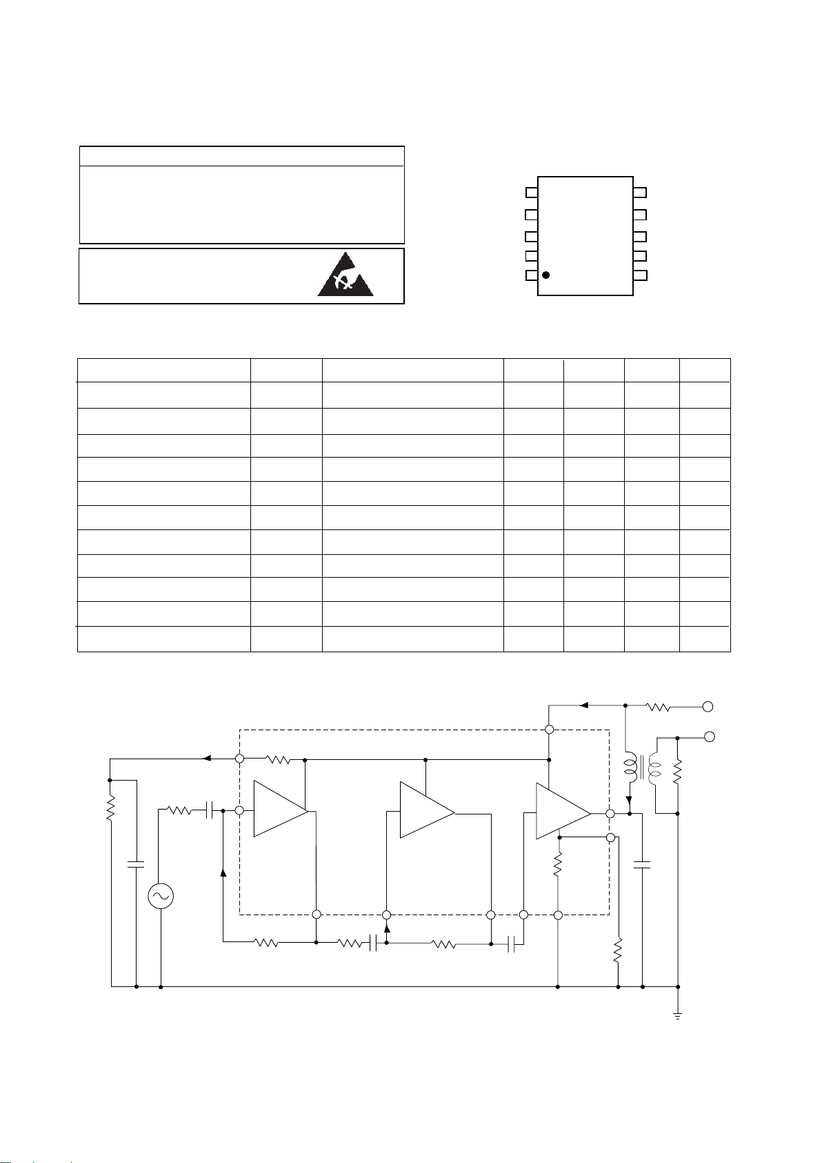
Fig. 1 Test Circuit
PARAMETER SYMBOL CONDITIONS MIN TYP MAX UNITS
Gain (Closed Loop) A
CL
V
OUT
= 500 VRMS 69 73 77 dB
Amplifier Current I
AMP
I
AMP = IA + IMIC
160 245 340 µA
Transducer Current I
TRANS H
RE = 47.5 1.1 1.3 1.7 mA
Transducer Current I
TRANS L
RE = ∞ 200 275 350 µA
Distortion THD V
OUT
= 500 VRMS -1 4 %
Input Referred Noise IRN NFB 0.2 to 10kHz at 12dB/Oct - 1 2 µV
Stable with Battery Resistance to R
B
- - 22 Ω
Input Bias Current I
B
-50 0 50 nA
On Chip Emitter Resistor R
E
- 200 - Ω
Emitter Bias Voltage (pin 8) V
RE
-54 -mV
Microphone Decoupling Resistor R
MIC
-4 -kΩ
ELECTRICAL CHARACTERISTICS
Conditions: Supply Voltage =1.3 VDC, Frequency = 1 kHz, Temperature = 25 oC
V
MIC
PIN CONNECTION
ABSOLUTE MAXIMUM RATINGS
PARAMETER VALUE / UNITS
Supply Voltage 5V DC
Power Dissipation 25 mW
Operating Temperature -10o to + 40oC
Storage Temperature -20o to + 70oC
CAUTION
CLASS 1 ESD SENSITIVITY
5
10
1
6
GND
B IN
A OUT
A IN
V
B
C OUT
R
E
C IN
B OUT
All switches and parameters remain as shown in Test Circuit unless otherwise stated in Conditions column.
All resistors in ohms, all capacitors in µF unless otherwise stated
VB=1.3 VDC
R1
2.7K
7
8
2
- B
- A
1.0
6
R
L
= 1K
R
MIC
4
3
1
R
FA
S
R
B =4.7
V
IN
I
B
33 K
- C
V
OUT
C
0.015
10
5
9
47.5K
1kHz
10
3.3 K
I
MIC
R
FB
I
B
56.2K
I
TRA NS
C
S
1.0
R
E =47.5
R
E
1.0
I
AMP
 Loading...