Gennum Corporation LD505, LC505 Datasheet

GENNUM
C O R P O R A T I O N
High Gain Class A Amplifier
LC505/LD505 DATA SHEET
FEATURES
• 71 dB of gain with 1.3 V supply
• 0.2 to 2.0 mA of transducer current adjustment
• 43 dB of volume control range
• 1.0 to 1.6 V supply operating range
• 2.2 k
Ω internal decoupling resistor for microphone
bias (LD505 only)
• output limiting capabilities (LD505 only)
STANDARD PACKAGING
• MINIpac P6 (LC505)
• MINIpac P8 (LD505)
DESCRIPTION
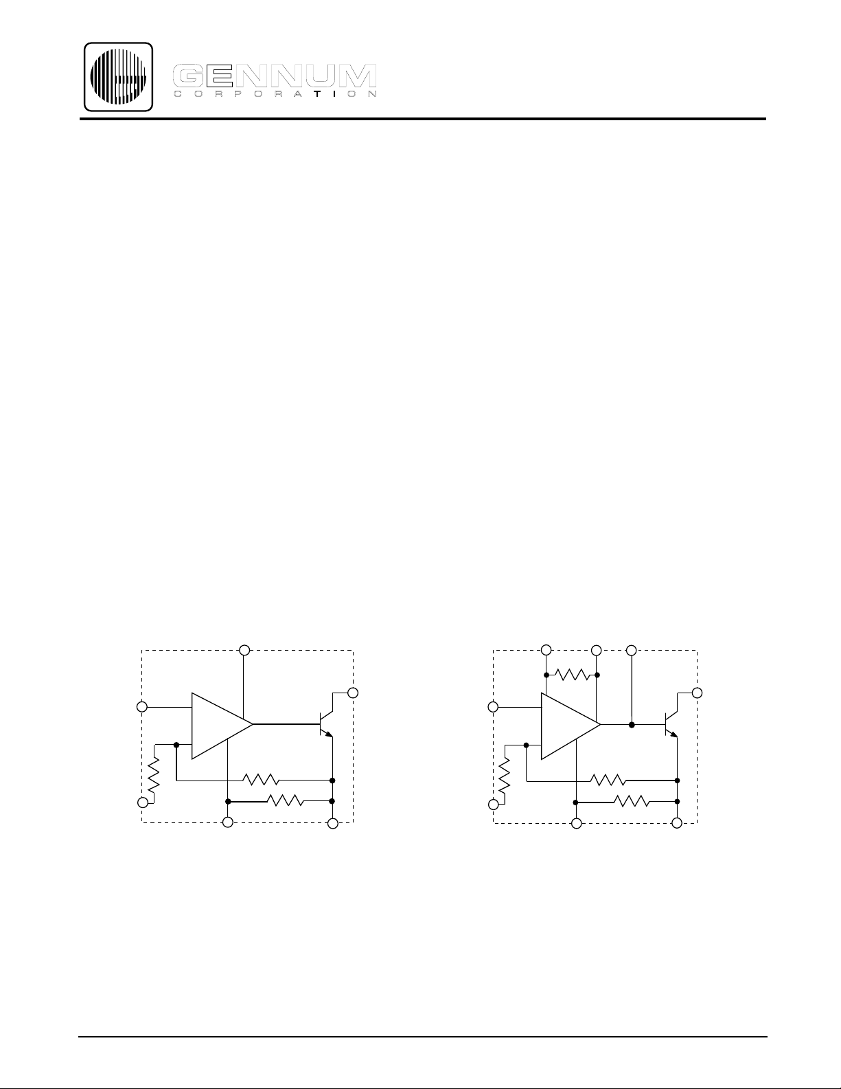
The LC/LD505 are low voltage, linear monolithic integrated
amplifiers with a typical electrical gain of 71 dB. The circuits
are comprised of a compensated, unconditionally stable,
operational amplifier and a low distortion Class A single
transistor output stage with negative feedback for stability
over a wide temperature range.
Current trimming in the output stage for inductive or resistive
loads can be accomplished by connecting an emitter resistor
from RE to ground. The LC/LD505 can operate over a supply
voltage range of 1.0 to 1.6 DC.
The LD505 which is an eight pin device, has an internal 2.2 kΩ
decoupling resistor for microphone bias providing increased
supply line rejection. The base of the output transistor is also
accessible allowing connection of diodes in a feedback
configuration for peak limiting.
VB
3
2
IN
NOT RECOMMENDED
5
VC
4
All resistors in ohms, all capacitors in
microfarads unless otherwise stated
Revision Date: January 1996
GENNUM CORPORATION P.O. Box 489, Stn A, Burlington, Ontario, Canada L7R 3Y3 tel. (905) 632-2996 fax: (905) 632-5946
Japan Branch: A-302, M iyamae Village, 2–10–42 M iyamae, Suginami–ku, Tokyo 168, Japan tel. (03) 3334-7700 fax (03) 3247-8839
+
-
FOR NEW DESIGNS
100
LC505 BLOCK DIAGRAM
33k
200
GND
RE
OUT
16
1
IN
VC
MIC
BIAS
6
5
All resistors in ohms, all capacitors in
microfarads unless otherwise stated
+
-
100
LD505 BLOCK DIAGRAM
2.2k
GND
VB
LIMITER
1
48
33k
200
RE
Document No. 500 - 15 - 09
3
OUT
27
500 - 15 - 09

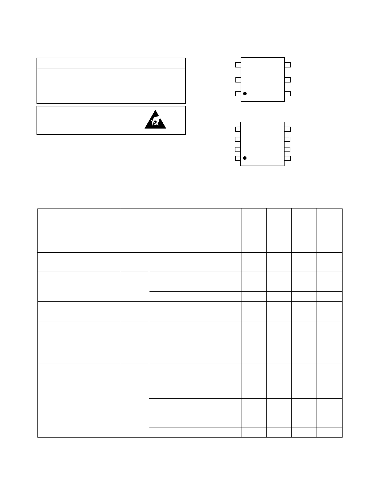
ABSOLUTE MAXIMUM RATINGS
PIN CONNECTION
PARAMETER VALUE & UNITS
V
3
B
VC
4
Supply Voltage 3 V
OUT
IN
Operating Temperature -10 to +40 °C
Power dissipation 25 mW
R
1
E
GND
6
LC505
CAUTION
CLASS 1 ESD SENSITIVITY
V
OUT
LIMITER
4
B
R
E
1
5
VC
IN
GND
MIC
8
BIAS
LD505
ELECTRICAL CHARACTERISTICS
All switches remain as shown in test circuit unless stated in condition column
Conditions: Temperature 25
PARAMETER SYMBOL CONDITIONS MIN TYP MAX UNITS
Gain A
Temperature Coefficient of Gain η
Amplifier Current I
Temperature Coefficient of Current η
Transducer Current I
Total Harmonic Distortion
Input Referred Noise Bandwidth at 12 dB/OCT - 0.2 to 10 kHz - 1.2 2.0 µVRMS
o
C, Vcc = 1.55 V
68 72 76 dB
V
A
V
= 1.3 V 66 71 76 dB
CC
- 0.07 - dB/oC
- 0.21 0.28 mA
A
Ι
Vcc = 1.3 V - 0.16 0.23 mA
- -0.002 - mA/oC
1.3 1.5 1.9 mA
L
Vcc = 1.3 V 1.0 1.3 1.7 mA
-25%
V
= 1.3 V - - 6 %
cc
Battery Resistance Stability RVC = 100k (S1-open) 22 - - Ω
Input Impedance
LC505 - 8 - kΩ
LD505 - 27 - kΩ
Low - 100 - Hz
Frequency Response (-3 dB)
High - 5000 - Hz
RVC = 0 to 100kΩ 36 43 - dB
(S1 - closed/open)
Volume Control Range RVC = 0 to 100kΩ 34 42 - dB
(S1 - closed/open) Vcc = 1.3 V
LC505 - -0.4 - dB/Ω
Gain Dependance of RB
500 - 15 - 09
LD505 - +0.16 - dB/Ω
2
 Loading...