Gennum Corporation GX9533-CTY, GX9533-CQY Datasheet

FEATURES
• operation beyond 622Mb/s
• accepts SMPTE and PECL input levels
• fully differential signal path
• on-chip PECL current loads eliminate need for
external pull-down resistors
• capable of driving 100Ω differential loads
• very low 500mW power consumption
• additional expansion port input for construction of
larger matrices
• auxiliary monitoring output
• easy to configure
• double latched address inputs with separate load and
configure
• TTL/CMOS compatible control logic inputs
• single 5V power supply
APPLICATIONS
Serial digital video switching; datacom or telecom
switching.
™
GX9533
GENLINX
II
Serial Digital 8x9 Crosspoint
DATA SHEET
DESCRIPTION
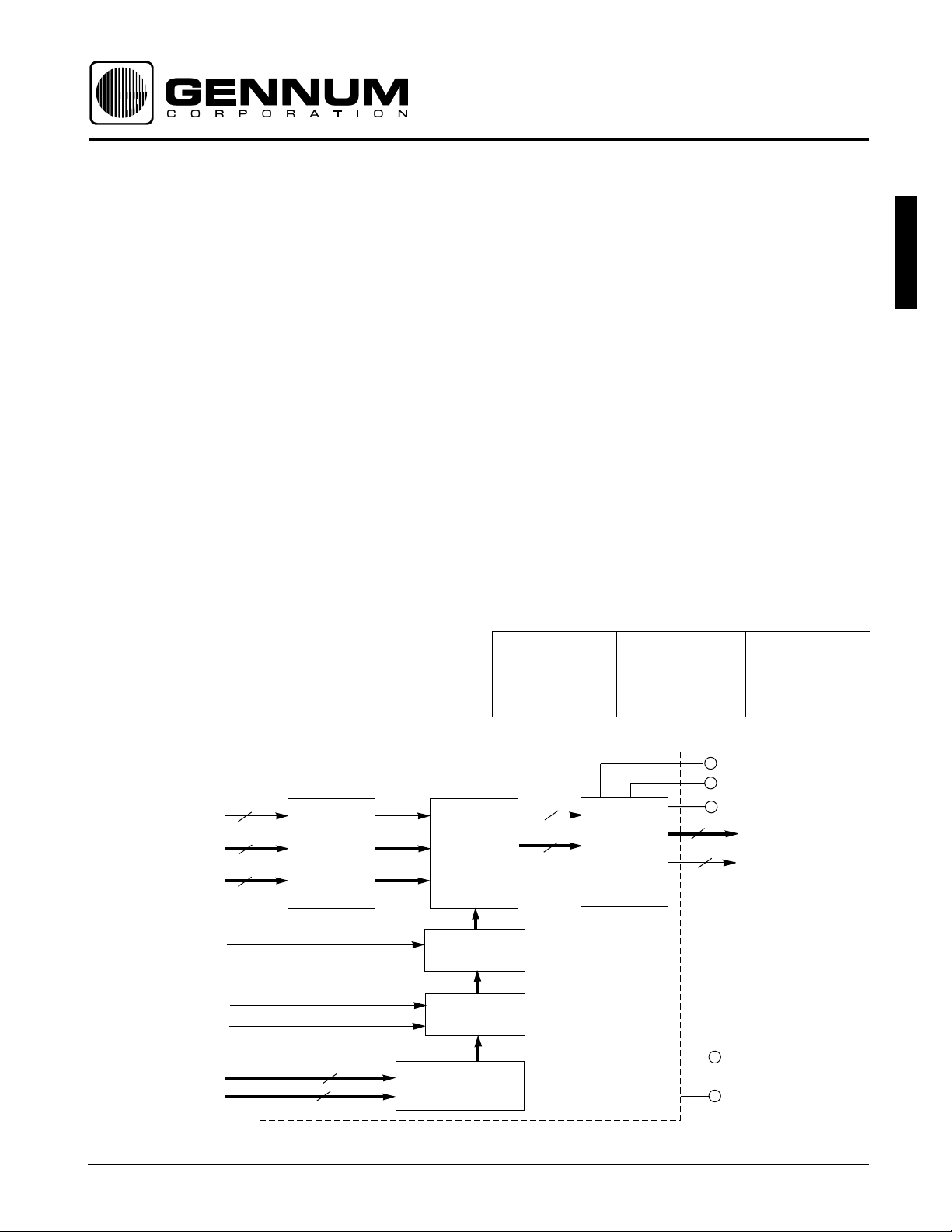
The GX9533 is a high speed 8x9 serial digital crosspoint.
An expansion input port eases the design of larger
switching matrices by reducing PCB layers and eliminating
the need for cascaded secondary switching. Decode logic
and double level latching to configure the matrix are
included on chip. Separate LOAD and CONFIGURE inputs
allow for asynchronous configuration and synchronous
switching. These latches can also be made transparent for
asynchronous switching by pulling the LOAD and
CONFIGURE pins high.
In the power saving (PS) mode, the GX9533 has a very low
power consumption of 500mW. This is accomplished by
driving a 400mV output swing into the on-chip 200Ω
differential load termination in the expansion port of the next
GX9533. This architecture provides a significant power
savings and the elimination of external load resistors or
impedance matching resistors. In applications where
standard PECL levels are necessary, the GX9533 can be
configured in "PECL Mode", to drive 800mV p-p into a 100Ω
differential load. The power consumption in this mode
increases to 860mW.
GX9533
AUX IN
EXP0..7
IN0 .. 7
CONFIG
LOAD
LOAD A
OA0..2
IA0..3
ORDERING INFORMATION
PART NUMBER PACKAGE TEMPERATURE
GX9533-CQY 100 pin MQFP Tray 0°C to 70°C
GX9533-CTY 100 pin MQFP Tape 0°C to 70°C
STD/PECL2
STD/PECL1
2
16
16
INPUT
BUFFER
3
4
SWITCHING
MATRIX
CONFIG
LATCH
LOAD
LATCH
DECODE
LOGIC
2
16
OUTPUT
BUFFER
V
CCO
16
OUT 0..7
2
AUX
V
EE
V
CC
BLOCK DIAGRAM
Revision Date: August 1999 Document No. 521 - 41 - 03
GENNUM CORPORATION P.O. Box 489, Stn. A, Burlington, Ontario, Canada L7R 3Y3
Tel. +1 (905) 632-2996 Fax. +1 (905) 632-5946 E-mail: info@gennum.com
www.gennum.com

ABSOLUTE MAXIMUM RATINGS
PARAMETER VALUE
Supply Voltage (V
= VCC-VEE)5.5V
S
Input Voltage Range (any input) -0.3 to (V
Power Dissipation 975mW
Operating Temperature Range 0°C to 70°C
Storage Temperature Range -65°C to +150°C
GX9533
Lead Temperature Range (soldering, 10 sec) 260°C
DC ELECTRICAL CHARACTERISTICS
VCC = 5V, VEE = 0V, TA = 0 to 70°C unless otherwise shown.
PARAMETER CONDITION MIN TYP MAX UNITS
Supply Voltage 4.75 5.0 5.25 V
ECL Input Voltage Swing 200 800 1200 mV p-p
ECL Common Mode Input Voltage Range with 1200mV input signal swing 2500 - V
Logic Input Voltage High 2.0 - V
Low 0 - 0.8 V
POWER SAVE 1 MODE
R
= 4k
Ω
SET
PARAMETER CONDITION MIN TYP MAX UNITS
CC
+0.3)V
-600 mV
CC
CC
V
Supply Current R
Output Common Mode Voltage V
= 100
L
Ω
- 115 150 mA
-1200 - VCC-800 mV
CC
Output Voltage Swing 300 450 600 mV
Output Voltage High V
Low V
-950 - VCC-600 mV
CC
-1400 - VCC-1000 mV
CC
POWER SAVE 2 MODE
R
= 6k
Ω
SET
PARAMETER CONDITION MIN TYP MAX UNITS
Supply Current R
Output Common Mode Voltage V
Output Voltage Swing 300 450 600 mV
Output Voltage High V
Low V
= 200
L
Ω
- 100 130 mA
-1200 - VCC-800 mV
CC
-950 - VCC-600 mV
CC
-1400 - VCC-1000 mV
CC
521 - 41 - 03
2

PECL MODE
R
= 2k
Ω
SET
PARAMETER CONDITION MIN TYP MAX UNITS
Supply Current R
Output Common Mode Voltage V
= 100
L
Ω
- 170 185 mA
-1450 - VCC-1050 mV
CC
Output Voltage Swing 700 800 900 mV
Output Voltage High V
Low V
-1200 - VCC-650 mV
CC
-1850 - VCC-1450 mV
CC
AC ELECTRICAL CHARACTERISTICS
VCC = 5.0V, VEE = 0V, TA = 0 to 70°C unless otherwise shown.
PARAMETER SYMBOL CONDITION MIN TYP MAX UNITS
Maximum Input Data Rate For 90% eye opening - 850 - Mb/s
Additive Jitter Standard
Input
Expansion
Input
Data In to Data Out
Delay
Standard
Input
Expansion
Input
Propagation Delay
Match
Standard
Input
t
DLY
143 to 622 Mb/s, all hostile
- 80 - ps p-p
crosstalk
- 70 - ps p-p
Average of all channels - 1.7 - ns
-1.1- ns
- 350 - ps
GX9533
Expansion
- 250 - ps
Input
CONFIGURE to Data
Main Out t
CD
-10-ns
Out Delay
AUX Out - 11 - ns
LOAD/LOADA Pulse Width t
CONFIGURE Pulse Width t
IA
to LOAD/LOADA High Setup Time t
N
LOAD/LOADA to IA
to LOAD High Setup Time t
OA
N
LOAD to OA
Low Hold Time t
N
Low Hold Time t
N
LOAD High to CONFIGURE High t
LP
CP
ILS
ILH
OLS
OLH
LC
20 - - ns
20 - - ns
30 - - ns
0--ns
30 - - ns
0--ns
0--ns
Output Rise/Fall Time - 700 - ps
NOTE
1. Use RMS addition to calculate additive jitter through cascaded devices.
3
521 - 41 - 03
 Loading...