Gennum Corporation GT4123BCDA, GT4123BCTA, GT4123BCKA Datasheet

Video Multiplier
DATA SHEET
GT4123B Two Channel
FEATURES
• two-quadrant video multiplication
• operation from
• 20 MHz
±0.1 dB video & control channel bandwidth
±4.5 V to ±13.2 V supply voltages
• ultra low differential gain & differential phase
• convenient 8 pin package
APPLICATIONS
• Multimedia Graphics Overlay
• Production Switchers
• Linear Keyers
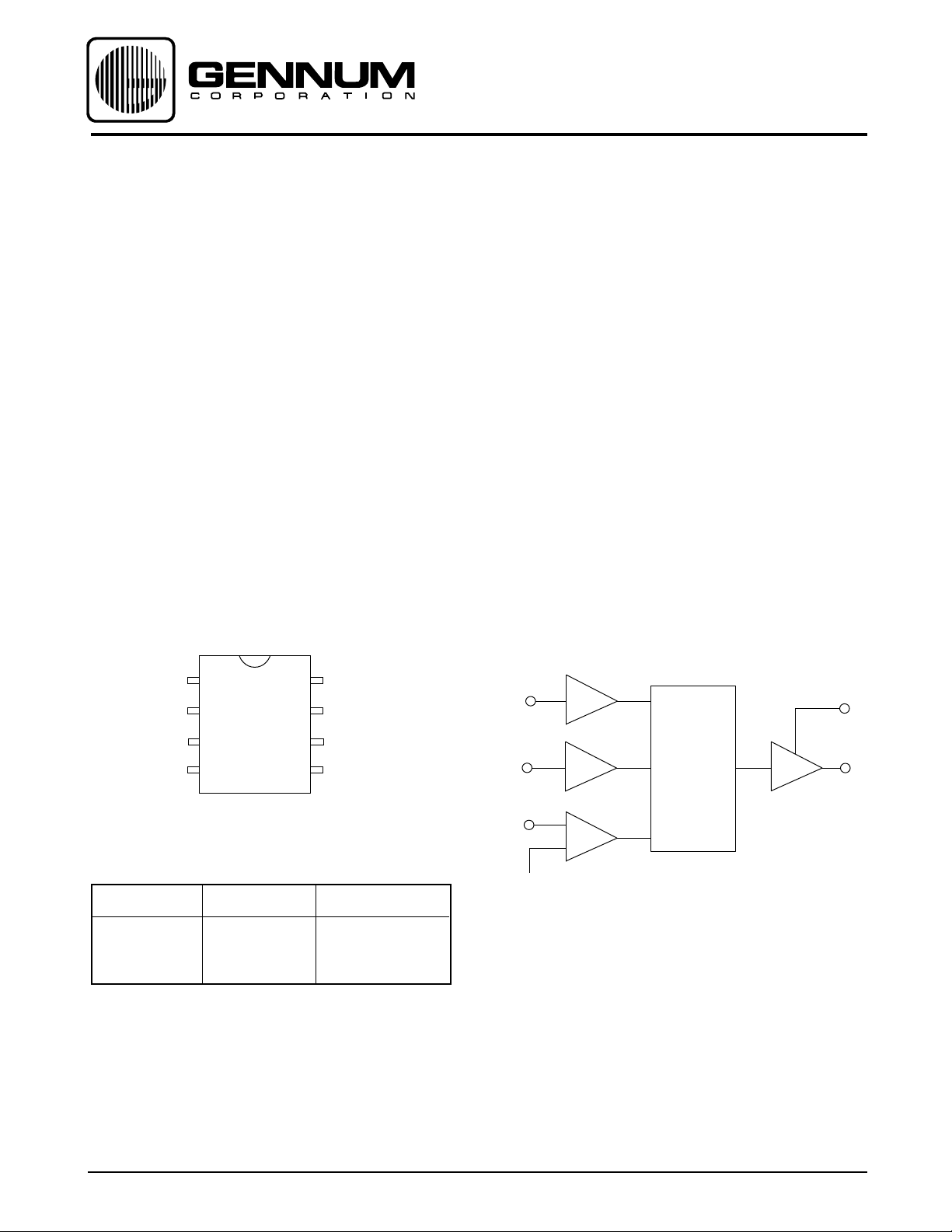
PIN CONNECTIONS
GT4123B
OUTPUT
FREQ. COMP
CONTROL
GROUND
1
2
3
4
8
7
6
5
V
cc
VIDEO IN B
V
EE
VIDEO IN A
DESCRIPTION
The GT4123B is a monolithic dual-channel video multiplier
for use in a wide range of applications including broadcast
and multimedia.
Featuring two wideband video inputs and a single control
input, the GT4123B achieves broadcast quality mixing of
two video input signals to a single output by implementing
the function:
V
= [ ( VC • VA) + (1 - VC) • VB ]
O
where V
continuously over the range 0 V to 1 V, and V
the video input signals.
is the control input voltage, which may be varied
C
and VB are
A
The GT4123B is a low power version of the GT4123 and
GT4123A Video Multipliers which operates from ±5 V
supply voltages and typically draws only 15 mA of current.
FUNCTIONAL BLOCK DIAGRAM
VIDEO IN A
VIDEO IN B
MULTIPLIER
CORE
FREQ
COMP
OUTPUT
CONTROL
ORDERING INFORMATION
V
(0.5V)
REF
Part Number Package Type Temperature Range
o
o
to 70
GT4123BCDA 8 pin PDIP 0
GT4123BCKA 8 pin SOIC 0
GT4123BCTA 8 pin SOIC Tape 0
o
to 70
o
to 70
C
o
C
o
C
GENNUM CORPORATION P.O. Box 489, Stn A, Burlington, Ontario, Canada L7R 3Y3 tel. (905) 632-2996 fax: (905) 632-2055
Japan Branch: A-302, Mi yamae Village, 2–10–42 Mi yamae, Suginami–ku Tokyo 168, Japan tel. (03) 3247-8838 fax (03) 3247-8839
(INTERNAL)
Document No. 521 - 20 - 01

ABSOLUTE MAXIMUM RATINGS
PARAMETER VALUE/UNITS
Supply Voltage ±13.5 V
Operating Temperature Range 0°C ≤ TA ≤ 70°C
Storage Temperature Range -65°C ≤ T
Lead Temperature (soldering, 10 seconds) 260°C
Video Input Voltage ±5 V
Control Input Voltage ±5 V
Video Input Differential Voltage ±5 V
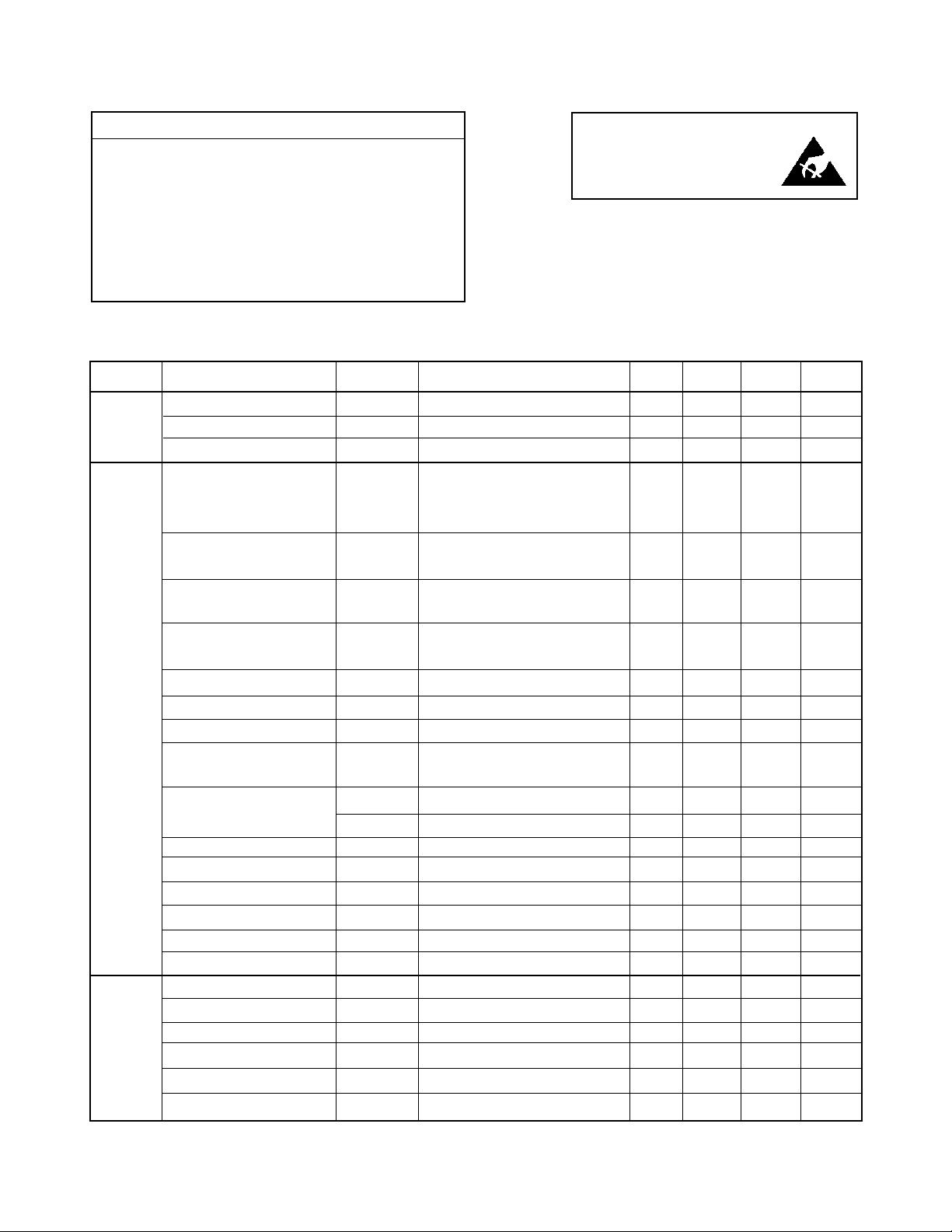
ELECTRICAL CHARACTERISTICS GT4123B
PARAMETER SYMBOL CONDITIONS MIN TYP MAX UNITS
POWER
SUPPLIES
SIGNAL
PATH
CONTROL
CHANNEL
NOTE: 1. V
521 - 20 - 01
Supply Voltage ± V
+ Supply Current I+ - 15 19.5 mA
- Supply Current I- - 15 19.5 mA
Common Mode Input Signal V
Bandwidth BW
Differential Gain ∂gV
Differential Phase ∂pV
PP Signal / RMS Noise S/N V
Gain A
Delay td
Power Supply Rejection PSRR ƒ = 1 kHz 70 - - dB
Ratio ƒ = 10 MHz 25 - - dB
Off Isolation & Crosstalk V
Output Offset Channel A or Channel B - - ±15 mV
Offset Difference Channel A - Channel B 0 - ±5mV
Input Resistance R
Input Capacitance C
Output Resistance R
Output Capacitance C
Bandwidth BW
Delay t
Linearity - - 1.5 %
Control Breakthrough VC = 0 to 1 V ƒ
Crossfade Balance VC = 0 to 1 V ƒ
Control Range V
= +1 Vp-p, output taken from OUTPUT
A or B
2 . V
= +1 Vp-p, output taken from V
C
S
IN CM
0.05
BW
0.1
V
SIG
A or B/VO
VC/V
A or B
IN
IN
OUT
OUT
at ±0.1 dB, V
0.1
D CONT
C
V
or
A
B
CAUTION
ELECTROSTATIC
SENSITIVE DEVICES
DO NOT OPEN PACKAGES OR HANDLE
EXCEPT AT A STATIC-FREE WORKSTATION
≤150°C
S
V
= ±5V, T
S
= 0°C to 70°C, RL=10kΩ, CL=10pF unless otherwise shown.
A
± 4.5 ±5 ±13.2 V
Supply Voltage = ±5 V
Positve Excursion Limit - - 2.2 V
Negative Excursion Limit - - -3.5 V
±0.05 dB, VIN= 150 mVp-p 10 - - MHz
±0.1 dB, V
= 40 IRE, 0V CM - 0.01 0.02 %
IN
= 150 mVp-p 20 25 - MHz
IN
at 3.58 MHz and 4.43 MHz
= 40 IRE, 0V CM - 0.01 0.03 deg
IN
at 3.58 MHz and 4.43 MHz
= 1 Vp-p, 60 70 - dB
SIG
100 kHz (ß = 100%) -0.02 -0.005 - dB
-410ns
ƒ
= 5 MHz (see note 1) 70 75 - dB
SIG
ƒ
= 5 MHz (see note 2) 80 85 - dB
SIG
ƒ=1 MHz 100 - - kΩ
- 2.0 - pF
ƒ=1 MHz - - 0.50 Ω
- 2.0 - pF
= 150 mVp-p 15 20 - MHz
IN
-410ns
=1 to 10 MHz - - -35 dB
C
= 3.58 MHz -15 0 +15 mV
C
0- +1V
2
 Loading...