GENLINX
Serial Digital Reclocker
FEATURES DEVICE DESCRIPTION
™
GS9015A
DATA SHEET
• reclocking of SMPTE 259M signals
• operational to 400 Mb/s
• adjustment free reclocker when used with the
GS9000B or GS9000S decoder and GS9010A
Automatic Tuning Sub-system
• 28 pin PLCC packaging
APPLICATIONS
• 4ƒ
, 4:2:2 and 360 Mb/s serial digital interfaces
SC
ORDERING INFORMATION
PART NUMBER PACKAGE TEMPERATURE
GS9015ACPJ 28 Pin PLCC 0O C to 70O C
GS9015ACTJ 28 Pin PLCC Tape 0O C to 70O C
The GS9015A is a monolithic IC designed to receive SMPTE
259M serial digital video signals. This device performs the
function of data and clock recovery. It interfaces directly with
the
GENLINX
™
GS9000B or GS9000S Decoder.
While there are no plans to discontinue the GS9015A, Gennum
has developed a successor product with improved features
and performance called the GS9035. The GS9035 is
recommended for new designs.
The VCO centre frequencies are controlled by external resistors
which can be selected by applying a two bit binary code to the
Standards Select input pins. Alternatively, the GS9015A can
be used with the GS9010A to form an adjustment free reclocker
system.
The GS9015A is packaged in a 28 pin PLCC operating from
a single +5 or -5 volt supply.
SPECIAL NOTE: R
reduced temperature range of T
and R
of T
are functional over the full temperature range
VCO3
=0°C to 70°C. This limitation does not affect
A
VCO1
and R
are functional over a
VCO2
=0°C to 50°C. R
A
VCO0
operation with the GS9010A ATS.
LOOP
FILTER
5,6
19
12
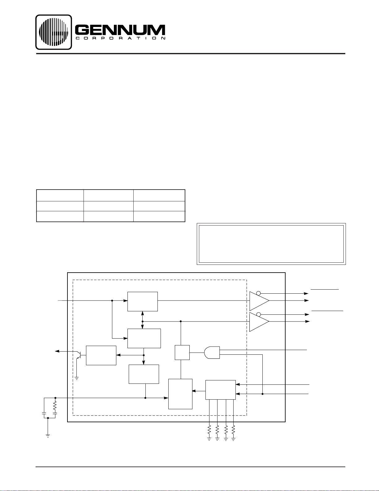
PLL
DIGITAL
IN
CARRIER
DETECT
Revision Date: April 1998
CARRIER
DETECT
DATA
LATCH
PHASE
COMPARATOR
÷2
CHARGE
PUMP
VCO
FUNCTIONAL BLOCK DIAGRAM
STANDARD
SELECT
131415
17
GS9015A
24
25
22
23
10
20
21
Document No. 520 - 99 - 05
SERIAL DATA
SERIAL DATA
SERIAL CLOCK
SERIAL CLOCK
ƒ/2
SS0
SS1
GENNUM CORPORATION P.O. Box 489, Stn. A, Burlington, Ontario, Canada L7R 3Y3 tel. +1 (905) 632-2996 fax. +1 (905) 632-5946
Web Site: www.gennum.com E-mail: info@gennum.com

ABSOLUTE MAXIMUM RATINGS
PARAMETER VALUE/UNITS
Supply Voltage 5.5 V
Input Voltage Range (any input) VCC+0.5 to VEE-0.5 V
EXCEPT AT A STATIC-FREE WORKSTATION
CAUTION
ELECTROSTATIC
SENSITIVE DEVICES
DO NOT OPEN PACKAGES OR HANDLE
DC Input Current (any one input) 5 mA
Power Dissipation 750 mW
Operating Temperature Range 0°C ≤ TA ≤70°C
Storage Temperature Range -65°C ≤ TS≤150°C
Lead Temperature (soldering, 10 seconds) 260°C
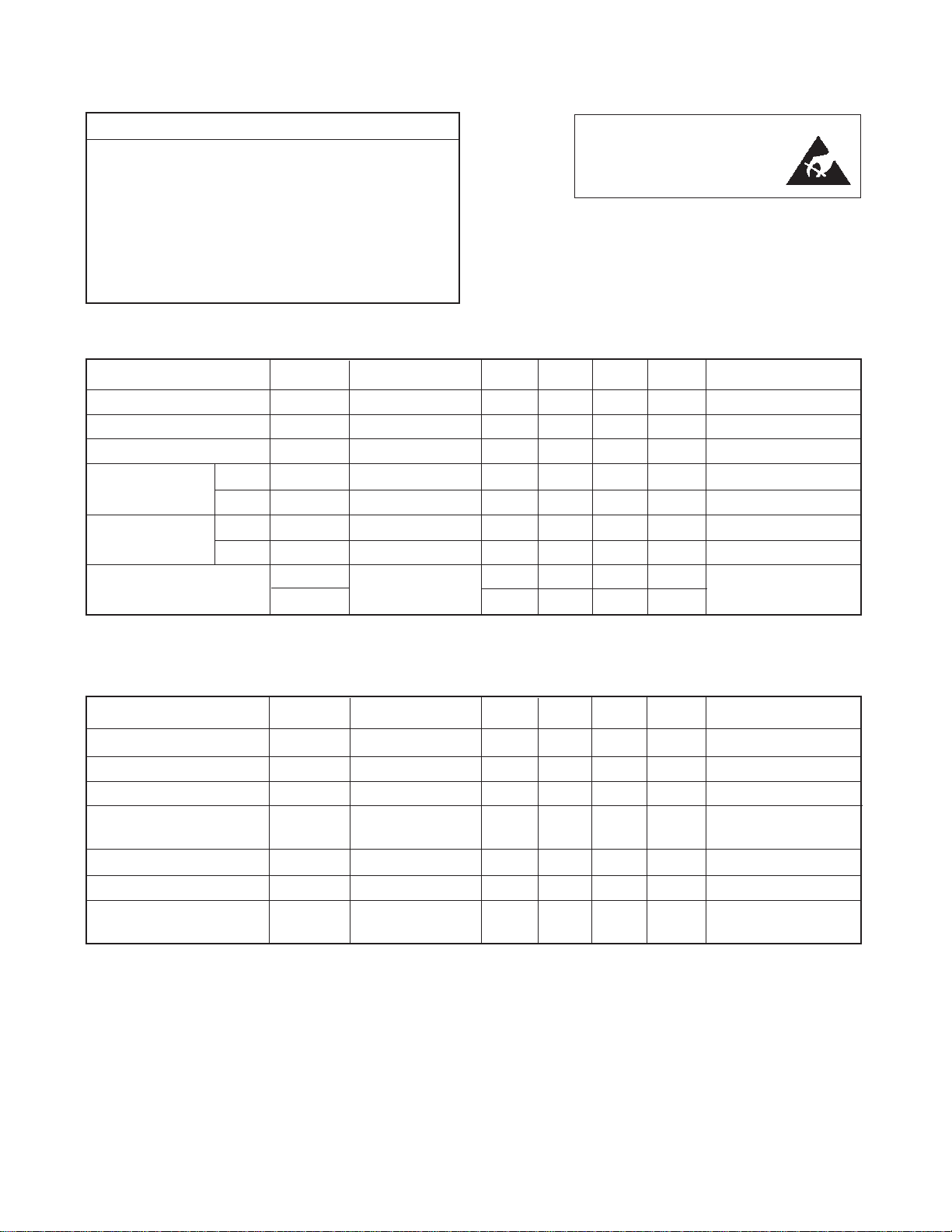
GS9015A RECLOCKER DC ELECTRICAL CHARACTERISTICS
VS = 5V, T
PARAMETER SYMBOL CONDITIONS MIN TYP MAX UNITS NOTES
Supply Voltage V
Power Consumption P
Supply Current (Total) I
Serial Data & - High V
Clock Output - Low V
Logic Inputs - High V
(1, 10, 20, 21)
- Low V
Carrier Detect V
Output Voltage V
= 0°C to 70°C, R
A
= 100Ω to (VCC - 2V) unless otherwise shown.
L
S
D
S
OH
OL
IH MIN
IL MAX
CDL
CDH
Operating Range 4.75 5.0 5.25 V
TA = 25°C -1.025 - -0.88 V with respect to V
TA = 25°C -1.9 - -1.6 V
R
= 10 kΩ to V
L
CC
- 330 500 mW
- 87 120 mA see Figure11
with respect to V
+2.0 - - V with respect to V
- - +0.8 V with respect to V
0.2 0.4 V
4.0 5.0 - V
with respect to VEE Open
Collector - Active High
CC
CC
EE
EE
GS9015A RECLOCKER AC ELECTRICAL CHARACTERISTICS
VS = 5V, TA = 0°C to 70°C, RL = 100Ω to (VCC - 2V) unless otherwise shown.
PARAMETER SYMBOL CONDITION MIN TYP MAX UNITS NOTES
Serial Data Bit Rate BR
Serial Clock Frequency ƒ
Output Signal Swing V
Serial Data to Serial Clock t
SDO
SLK
O
d
Synchronization
Lock Times t
Jitter t
Direct Digital Input V
LOCK
J
DDI
Levels (5, 6)
NOTES: 1. Switching between two sources of the same data rate.
TA = 25°C 100 - 400 Mb/s
TA = 25°C 100 - 400 MHz see Figure 9
TA = 25°C 700 800 900 mV p-p see Figure10
See Waveforms - -500 - ps Data lags Clock
see note 1 - - 10 µs
TA= 25°C, 270 Mb/s - ±100 - ps p-p see Figure12
200 - 2000 mVp-p Differential Drive
520 - 99 - 05
2

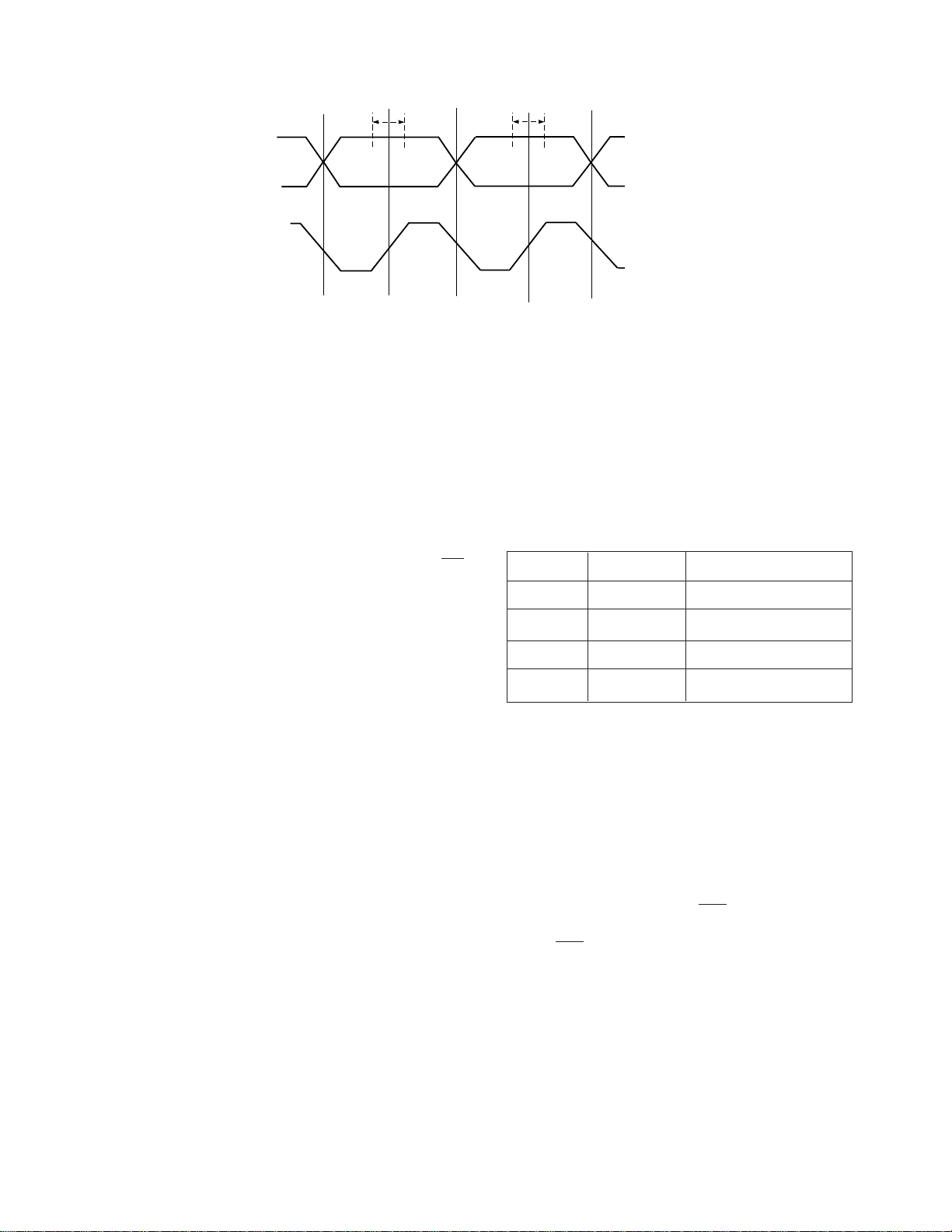
SERIAL
DATA OUT
(SD0)
t
D
t
D
SERIAL
CLOCK OUT
(SCK)
50%
Fig.1 Waveforms
GS9015A Reclocking Receiver - Detailed Device Description
The GS9015A Reclocking Receiver is a bipolar integrated
circuit containing circuitry necessary to re-clock and regenerate
the NRZI serial data stream.
Packaged in a 28 pin PLCC, the receiver operates from a
single five volt supply at data rates to 400 Mb/s. Typical power
consumption is 330 mW. Typical output jitter is ±100 ps at
270 Mb/s.
Serial Digital signals are applied to digital inputs DDI and DDI
(pins 5,6).
Phase Locked Loop
The phase comparator itself compares the position of
transitions in the incoming signal with the phase of the local
oscillator (VCO). The error-correcting output signals are fed
to the charge pump in the form of short pulses. The charge
pump converts these pulses into a “charge packet” which is
accurately proportional to the system phase error.
The charge packet is then integrated by the second-order
loop filter to produce a control voltage for the VCO.
50%
VCO Centre Frequency Selection
The centre frequency of the VCO is set by one of four external
current reference resistors (RVCO0-RVCO3) connected to
pins 13,14,15 or 17. These are selected by two logic inputs
SS0 and SS1 (pins 20, 21) through a 2:4 decoder according
to the following truth table.
SS1 SS0 Resistor Selected
0 0 RVCO0 (13)
0 1 RVCO1 (14)
1 0 RVCO2 (15)
1 1 RVCO3 (17)
As an alternative, the GS9010A Automatic Tuning Sub-system
and the GS9000B or GS9000S Decoder may be used in
conjunction with the GS9015A to obtain adjustment free and
automatic standard select operation (see Figure17).
During periods when there are no transitions in the signal, the
loop filter voltage is required to hold precisely at its last value
so that the VCO does not drift significantly between corrections.
Commutating diodes in the charge pump keep the output
leakage current extremely low, minimizing VCO frequency
drift.
The VCO is implemented using a current-controlled
multivibrator, designed to deliver good stability, low phase
noise and wide operating frequency capability. The frequency
range is design-limited to ±10% about the oscillator centre
frequency.
With the VCO operating at twice the clock frequency, a clock
phase which is centred on the eye of the locked signal is used
to latch the incoming data, thus maximising immunity to
jitter-induced errors. The alternate phase is used to latch the
output re-clocked data SDO and SDO (pins 25, 24). The true
and inverse clock signals themselves are available from the
SCO and SCO pins 23 and 22.
3
520 - 99 - 05

V
V
V
EE1
EE1
EE1
V
EE1
V
EE1
V
EE2
V
CC3
DDI
DDI
V
CC1
V
V
EE1
ƒ/2 EN
V
EE3
EE1
4 3 2 28 27 26
5
6
7
8
9
10
11
12 13 14 15 16 17 18
LOOP R
VCO0
FILT
GS9015A
TOP VIEW
R
VCO1 RVCO2
V
EE3
R
VCO3
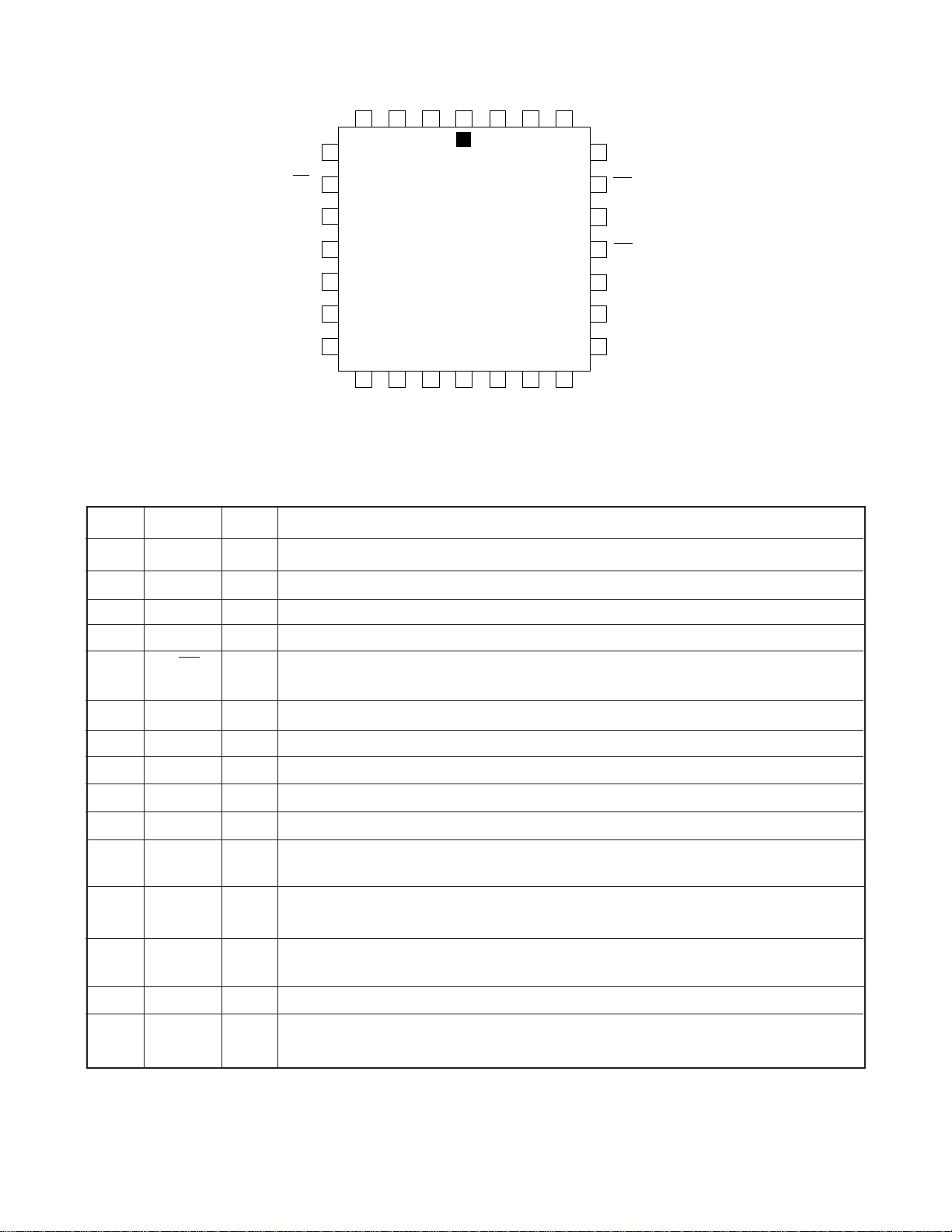
Fig. 2 GS9015A Pin Connections
GS9015A PIN DESCRIPTIONS
PIN NO. SYMBOL TYPE DESCRIPTION
1V
EE1
Power Supply. Most negative power supply connection.
SD0
25
SD0
24
SC0
23
SC0
22
SS1
21
SS0
20
CD
19
V
CC2
2V
3V
4V
EE1
EE1
EE1
Power Supply. Most negative power supply connection.
Power Supply. Most negative power supply connection.
Power Supply. Most negative power supply connection.
5,6 DDI/DDI Input Direct Data Inputs (true and inverse). Pseudo-ECL, differential serial data inputs. They may be
7V
8, 9 V
CC1
EE1
directly driven from true ECL drivers when VEE = -5V and V
Power Supply. Most positive power supply connection. (Phase Detector, Carrier Detect).
Power Supply. Most negative power supply connection.
CC
= 0 V.
10 ƒ/2 EN Input ƒ/2 Enable-TTL compatible input used to enable the divide by 2 function.
11 V
EE3
Power Supply. Most negative power supply connection. (VCO, MUX, Standard Select)
12 LOOP FILT Loop Filter. Node for connecting the loop filter components.
13 R
VCO0
Input VCO Resistor 0. Analog current input used to set the centre frequency of the VCO when the two
Standard Select bits (pins 20 and 21) are set LOW. A resistor is connected from this pin to VEE.
14 R
VCO1
Input VCO Resistor 1. Analog current input used to set the centre frequency of the VCO when Standard
Select bit 0 (pin 20) is set HIGH and bit 1 (pin 21) is set LOW. A resistor is connected from this pin to VEE.
15 R
VCO2
Input VCO Resistor 2. Analog current input used to set the centre frequency of the VCO when Standard
Select bit 0 (pin 20) is set LOW and bit 1 (pin 21) is set HIGH. A resistor is connected from this pin to VEE.
16 V
17 R
EE3
Input VCO Resistor 3. Analog current input used to set the centre frequency of the VCO when the two
VCO3
Power Supply. Most negative power supply connection.
Standard Select bits (pins 20 and 21) are set HIGH. A resistor is connected from this pin to VEE.
520 - 99 - 05
4
 Loading...