Gennum Corporation GS1522-CQR Datasheet
™
HD-LINX
GS1522
HDTV Serial Digital Serializer
PRELIMINARY DATA SHEET
FEATURES
• SMPTE 292M compliant
• 20:1 parallel to serial conversion
• NRZ(I) encoder & SMPTE scrambler with selectable
bypass
• NRZ to NRZ(I) serial data conversion
• 1.485Gb/s and 1.485/1.001G b/s oper a tion
• lock detect output
• selectable DUAL or QUAD 75Ω cable driver outputs
• 8 bit or 10 bit input data support
• 20 bit wide inputs
• 3.3V and 5V CMOS/TTL compatible inputs
• single +5.0V power supply
APPLICATIONS
SMPTE 292M Serial Digital Interfaces for Video Cameras,
Camcorders, VTR's, Signal Generators, Portable Equipment, and NLE's.
ORDERING INFORMATION
PART NUMBER PACKAGE TEMPERATURE
GS1522-CQR 128 pin MQFP 0°C to 70°C
DESCRIPTION
The GS1522 is a monolithic bipolar integrated circuit
designed to serialize SMPTE 274M and SMPTE 260M bit
parallel digital signals.
This device performs the following functions:
• Sync word mapping for 8-bit/10-bit operation.
• Parallel to Serial conversion of Luma & Chroma data
• Interleaving of Luma and Chroma data
9+X4
• Data Scrambling (using the X
+1 algorithm)
• Conversion of NRZ to NRZI serial data (using the (X+1)
algorithm)
• Selectable DUAL or QUAD 75Ω Cable Driver outputs
• Lock Detect Output
• 1.485Gb/s or 1.485/1.001Gb/s operation
This device requires a single 5V supply and typically
consumes less than 1000mW of power while driving two
75Ω cables.
The GS1522 uses the GO1515 external VCO connected to
the internal PLL circuitry to achieve ultra low noise PLL
performance.
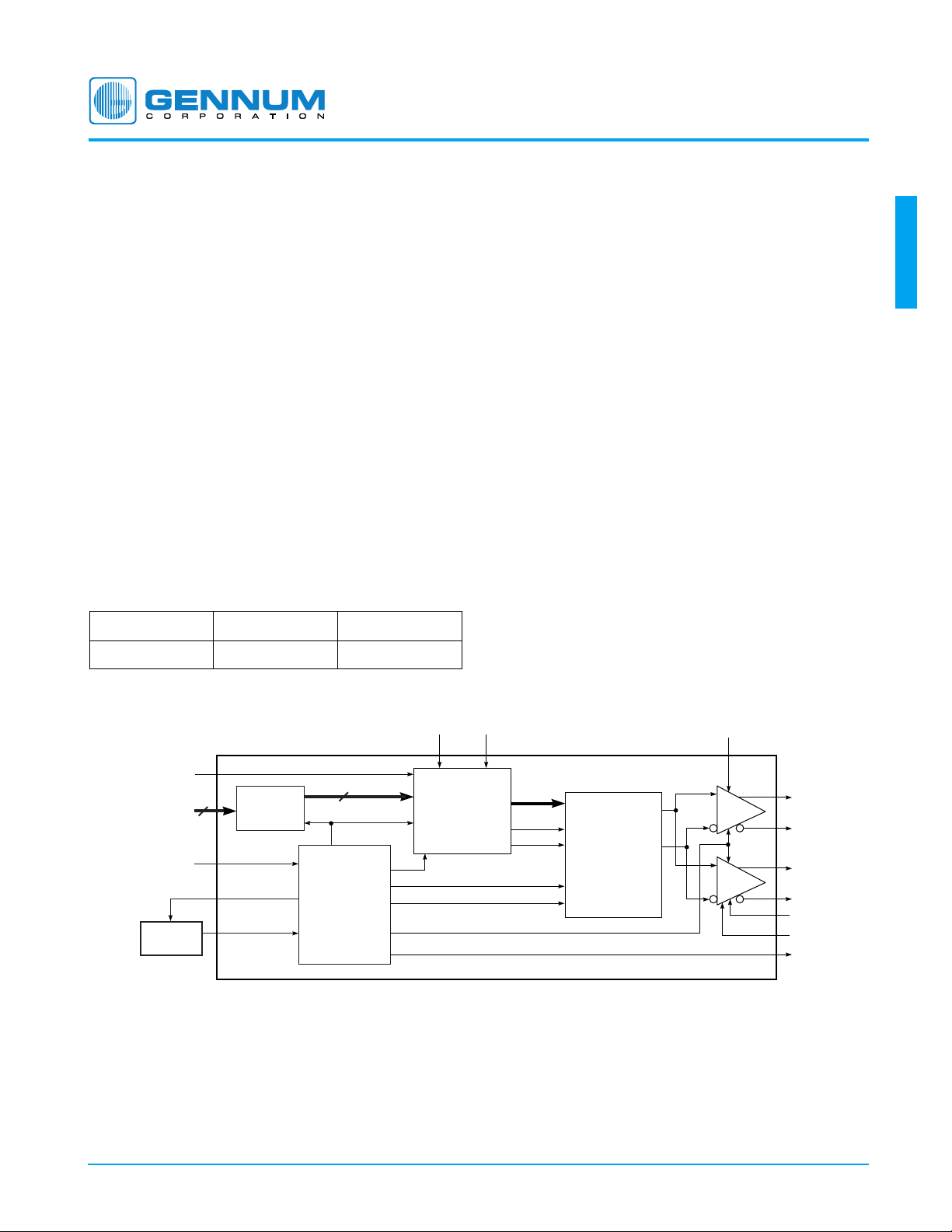
GS1522
SYNC_DETECT
_DISABLE
DATA_IN[19:0]
PCLK_IN
GO1515
BYPASSRESET
20
INPUT
LATCH
20
PLL
SYNC DETECT
SMPTE
SCRAMBLER
INTERLEAVER
RESET
BYPASS
S
CLK
P
LOAD
PARALLEL
TO SERIAL
CONVERTER
NRZ TO NRZI
MUTE
R
O/P0
O/P1
SET0
SDO0+
SDO0-
SDO1+
SDO1R
SET1
SDO1_EN
PLL_LOCK
FUNCTIONAL BLOCK DIAGRAM
Revision Date: August 2000 Document No. 522 - 26 - 00
GENNUM CORPORATION P.O. Box 489, Stn. A, Burlington, Ontario, Canada L7R 3Y3
Tel. +1 (905) 632-2996 Fax. +1 (905) 632-5946 E-mail: info@gennum.com
www.gennum.com
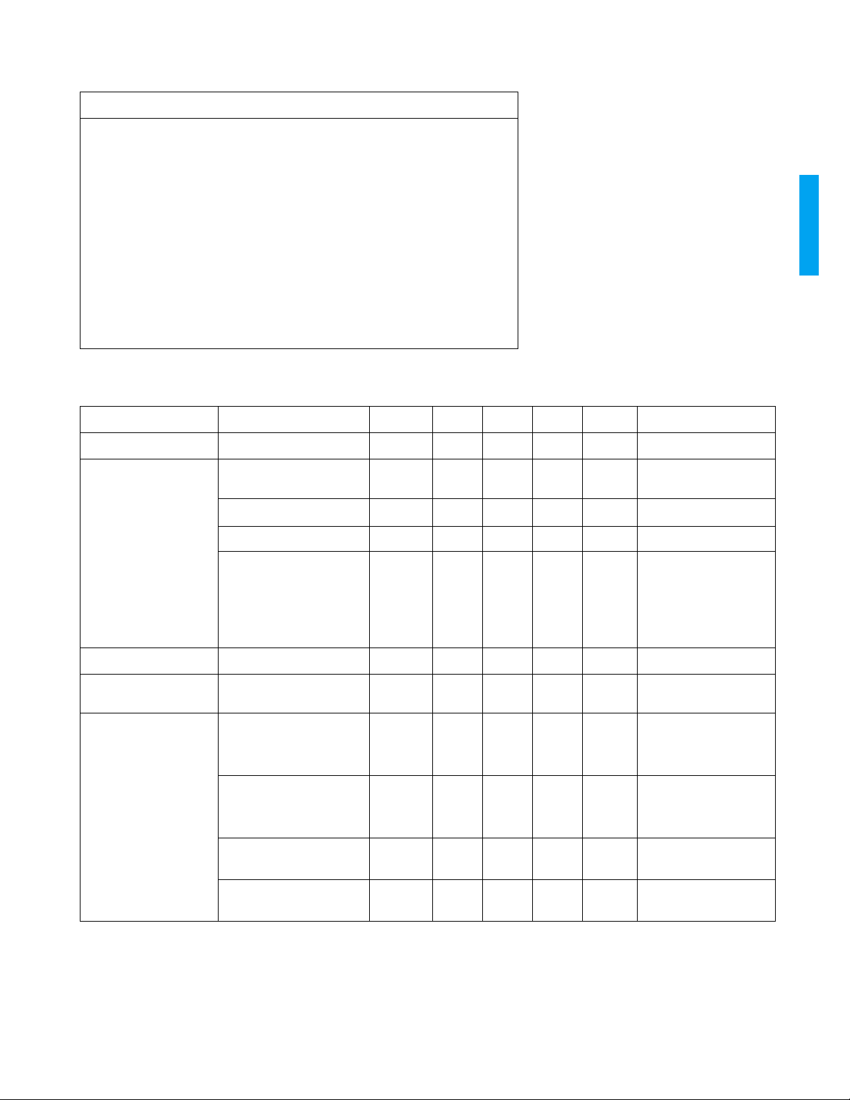
ABSOLUTE MAXIMUM RATINGS
PARAMETER VALUE
Supply Voltage (V
Input Voltage Range (any input) V
)5.5V
S
– 0.5 < VIN < VCC+ 0.5
EE
DC Input Current (any input) TBD
Power Dissipation (V
= 5.25V) TBD
CC
Input ESD Voltage TBD
Die Temperature 125°C
Operating Temperature Range 0°C ≤ T
Storage Temperature Range -40°C ≤ T
≤ 70°C
A
≤ 150°C
S
Lead Temperature (soldering 10 seconds) 260°C
AC ELECTRICAL CHARACTERISTICS
VCC = 5V, VEE = 0V, TA = 0°C to 70°C unless otherwise specified.
PARAMETER CONDITIONS SYMBOL MIN TYP MAX UNITS NOTES
Serial data bit rate SMPTE 292M BR
Digital Serial Data
Differential outputs V
Outputs
Rise/Fall times, 20-80% t
SDO
, t
r
SDO
f
- 1.485 - Gb/s 1.485/1.001Gb/s also
750 800 850 mV p-p With 52.3Ω 1% R
- 150 270 ps
GS1522
SET
Resistor
Overshoot - 0 7 %
Output Return Loss @
1.485GHz
Lock Time Worst case t
Typical Loop Bandwidth≤ 0.1dB peaking,
1.485Gb/s
Intrinsic Jitter Pseudo-random
23
PRBS (2
-1)
(200kHz LBW)
Pathological
PRBS (2
23
-1)
(200kHz LBW)
Pseudo-random
(1.5 MHz LBW)
Pathological
(1.5 MHz LBW)
ORL 15 17 - dB As per SMPTE292M
(5MHz to clock
frequency), using
Gennum Evaluation
Board, recommended
layout and components.
LOCK
- 200 250 ms
- 0.200 1.5 MHz
t
IJR
t
IJP
t
IJR
t
IJP
- - 100 ps p-p
- - 100 ps p-p
- - 100 ps p-p
- - 100 ps p-p
GENNUM CORPORATION
2
522 - 26 - 00
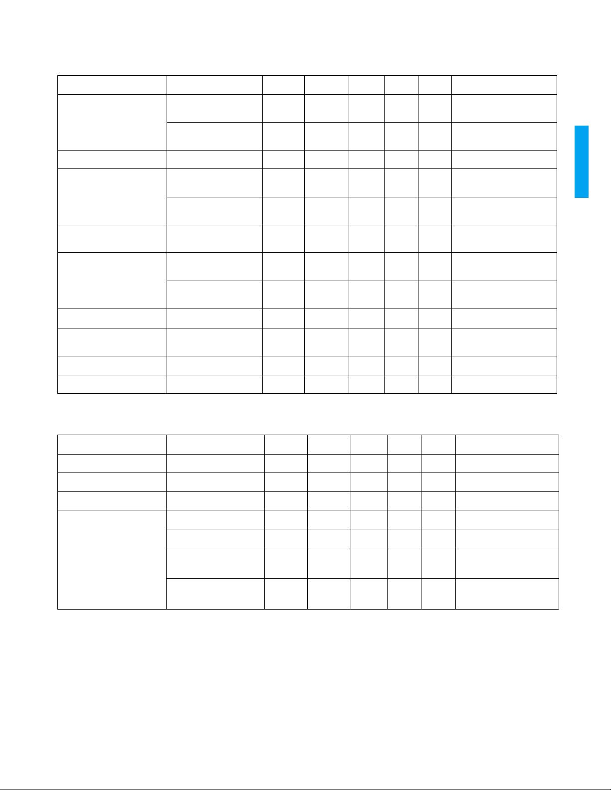
AC ELECTRICAL CHARACTERISTICS - PARALLEL TO SERIAL STAGE
VDD = 5V, TA = 0°C to 70°C unless otherwise specified.
PARAMETER CONDITIONS SYMBOL MIN TYP MAX UNITS NOTES
Input Voltage Levels V
Input Capacitance C
Output Voltage Levels V
Parallel Input Clock
P
Frequency
Input Clock Pulse Width
Low
Input Clock Pulse Width
High
Input Clock Rise/Fall time t
Input Clock Rise/Fall time
Matching
Input Setup Time t
Input Hold Time t
IL
V
IH
IN
OL
V
OH
CLK_IN
t
PWL
t
PWH
, t
r
f
t
rfm
SU
IH
- - 0.8 V For compatibility with TTL
voltage levels
2.0 - - V For compatibility with TTL
voltage levels
-12pF
- - 0.4 V For compatibility with TTL
voltage levels
2.4 - - V For compatibility with TTL
voltage levels
- 74.25 - MHz 74.25/1.001MHz also
5--ns
5--ns
- 500 1000 ps 20% to 80%
- 200 - ps
1.0 - - ns
0--ns
GS1522
DC ELECTRICAL CHARACTERISTICS
VCC = 5V, VEE = 0V, TA = 0°C to 70°C unless otherwise specified.
PARAMETER CONDITIONS SYMBOL MIN TYP MAX UNITS NOTES
Positive Supply Voltage Operating Range V
Power (system power) V
Supply Current V
= 5.00V, T=25°C P
CC
V
= 5.00V, T=25°C P
CC
= 5.25V, T=70°C - - 300 mA (Driving four 75Ω outputs)
CC
= 5.00V, T=25°C - 234 - mA (Driving four 75Ω outputs)
V
CC
SDO1 disabled
= 5.25V, 70°C
V
CC
SDO1 disabled
V
= 5.0V, 25°C
CC
CC
4.75 5.00 5.25 V
D
D
- 950 - mW (Driving two 75Ω outputs)
- 1170 - mW (Driving four 75Ω outputs)
- - 240 mA (Driving two 75Ω outputs)
- 190 - mA (Driving two 75Ω outputs)
GENNUM CORPORATION
3
522 - 26 - 00
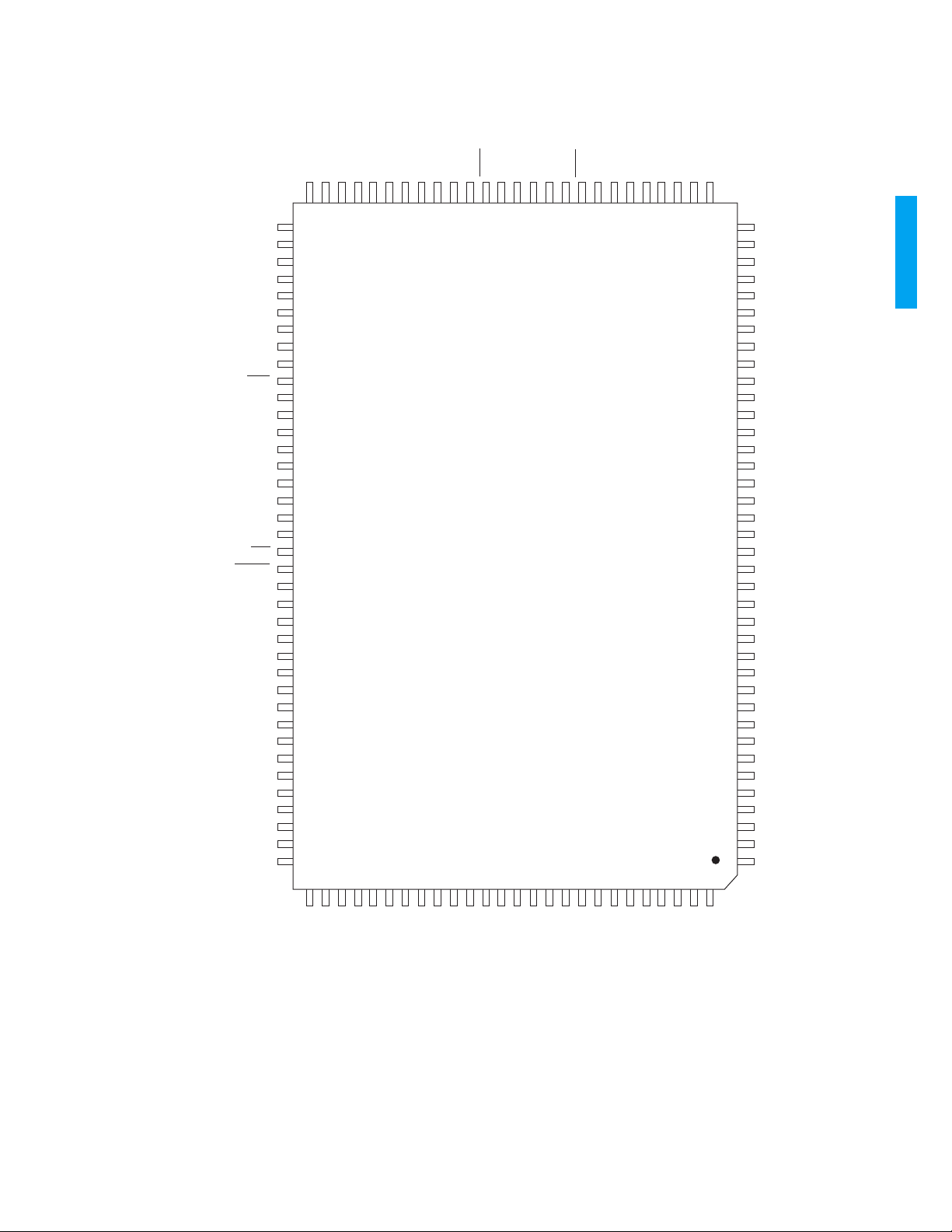
PIN CONNECTIONS
NC
NC
NC
NC
NC
NC
NC
NC
NC
VCO
VCO
PD_V
PDSUB_V
EE
EE
IJI
PD_V
CC
NC
NC
LFS
NC
LFS
PLCAP
DM
PLCAP
DFT_V
EE
LFA_V
EE
LFA
LBCONT
LFA_V
CC
NC
V
CC3
V
EE3
SYNC_DETECT_DISABLE
NC
NC
NC
NC
NC
NC
OSC_VEEA0NCNCNCV
EE2
SET0
R
CC2
V
NC
SDO0
SDO_NC
SDO0NCNCNCSDO1
SDO_NC
SDO1NCV
SET1
CC2
R
NCNCNCNCNC
64636261605958575655545352515049484746454443424140
65
66
67
68
69
70
71
72
73
74
75
76
77
78
79
80
81
82
83
GS1522
TOP
VIEW
84
85
86
87
88
89
90
91
92
93
94
95
96
97
98
99
100
101
102
103
104
105
106
107
108
109
110
111
112
113
114
115
116
117
118
119
120
121
122
123
124
125
126
127
39
38
37
36
35
34
33
32
31
30
29
28
27
26
25
24
23
22
21
20
19
18
17
16
15
14
13
12
11
10
128
9
8
7
6
5
4
3
2
1
NC
NC
NC
NC
NC
NC
NC
SDO1_EN
V
EE2
V
EE2
V
EE2
V
EE2
V
EE2
V
CC2
V
CC2
V
CC2
V
CC2
V
CC2
NC
NC
V
EE2
RESET
BYPASS
PLL_LOCK
NC
XDIV20
NC
NC
BUF_V
EE
NC
NC
NC
NC
NC
NC
NC
PCLK_IN
V
EE3
GS1522
NC
NC
DATA_IN[19]
DATA_IN[18]
DATA_IN[17]
DATA_IN[16]
DATA_IN[15]
NOTE: No Heat Sink Required
DATA_IN[14]
DATA_IN[13]
DATA_IN[12]
DATA_IN[11]
DATA_IN[9]
DATA_IN[10]
NC
NC
DATA_IN[8]
DATA_IN[7]
NC
NC
DATA_IN[6]
DATA_IN[5]
DATA_IN[4]
DATA_IN[3]
DATA_IN[2]
DATA_IN[1]
DATA_IN[0]
4
GENNUM CORPORATION
522 - 26 - 00

PIN DESCRIPTIONS
NUMBER SYMBOL LEVEL TYPE DESCRIPTION
1, 95 V
EE3
Power Input
2 PCLK_IN TTL Input
3, 4, 5, 6, 7, 8,
NC
9, 11, 12, 14,
19, 20, 32, 33,
34, 35, 36, 37,
38, 39, 40, 41,
42, 43,46, 50,
51, 52, 56, 60,
61, 62, 65, 66,
67, 68, 69, 70,
71, 72, 73, 80,
81, 83, 93, 97,
98, 99, 100,
101, 102, 108,
109, 116, 117,
120, 121
10 BUF_V
EE
Power TEST
13 XDIV20 TTL TEST
15 PLL_LOCK TTL Output
Negative Supply.
Most negative power supply connection, for
input stage.
Parallel Data Clock
No Connect
. 74.25 or 74.25/1.001MHz
. These pins are not used internally. These pins
should be floating.
Negative Supply/Test Pin
. Most negative power supply
connection. For buffer for oscillator/divider for test purposes only.
Leave floating for normal operation.
. Test block output. Leave floating for normal operation.
Test Pin
Status Signal Output
. Indicates when the GS1522 is phase locked
to the incoming PCLK_IN clock signal. LOGIC HIGH indicates
PLL is in Lock. LOGIC LOW indicates PLL is out of Lock.
GS1522
16 BYPASS TTL Input
17 RESET TTL Input
18, 26, 27, 28,
V
EE2
Power Input
29, 30, 59
21, 22, 23, 24,
V
CC2
Power Input
25, 45, 57
31 SDO1_EN Power Input
44 R
SET1
Input
47, 49 SDO1+, SDO1- Analog Output
48, 54 SDO_NC
Control Signal Input
. Used to bypass the scrambling function if
data is already scrambled by GS1501 or if non-SMPTE encoded
data stream such as 8b/10b is to be transmitted. When BYPASS is
LOW, the SMPTE scrambler and NRZ(I) encoder are enabled.
When BYPASS is HIGH, the SMPTE scrambler and NRZ(I) encoder
are bypassed.
Control Signal Input
. Used to reset the SMPTE scrambler. For
logic HIGH; Resets the SMPTE scrambler and NRZ(I) encoder.
For logic LOW: normal SMPTE scrambler and NRZ(I) encoder
operation.
Negative Supply
. Most negative power supply connection. For
Cable Driver outputs and all other digital circuitry excluding input
stage and PLL stage.
Positive Supply
. Most positive power supply connection. For
Cable Driver outputs and all other digital circuitry excluding input
stage and PLL stage.
Control Signal Input
. Used to enable or disable the second serial
data output stage. This signal must be tied to GND to enable this
stage. Do not connect to a logic low.
Control Signal Input
output amplitude for SDO1 and SDO1
Serial Data Output Signal
Use 75Ω ±1% pull up resistors to V
No Connect
. External resistor is used to set the data
. Use a ±1% resistor.
. Current mode serial data output #1.
CC2
.
. Not used internally. This pin must be left floating.
53, 55 SDO0+, SDO0- Analog Output
GENNUM CORPORATION
Serial Data Output Signal
. Current mode serial data output #0.
Use 75Ω ± 1% pull up resistors to V
5
CC2
.
522 - 26 - 00
PIN DESCRIPTIONS (Continued)
NUMBER SYMBOL LEVEL TYPE DESCRIPTION
58 R
SET0
Analog Input
63 A0 TTL TEST
64 OSC_V
74 VCO
EE
Power Input
Analog Input
75 VCO Analog Input
76 PD_V
77 PDSUB_V
EE
EE
Power Input
Power Input
78 IJI Analog Output
79 PD_V
CC
82, 84 LFS, LFS
85, 87 PLCAP, PLCAP
Power Input
Analog Input
Analog Input
Control Signal Input
output amplitude for SDO0 and SDO0
Test Signal
. Used for manufacturing test purposes only. This pin
. External resistor is used to set the data
. Use a ±1% resistor.
must be tied low for normal operation.
Negative Supply
. Ground for ring oscillator. This pin must be
floating for normal operation.
Control Signal Input
. Input pin is AC coupled to ground using a
50Ω transmission line.
Control Signal Input
. Voltage controlled oscillator input. This pin is
connected to the output pin of the GO1515 VCO. This pin must be
connected to the GO1515 VCO output pin via a 50Ω transmission
line.
Negative Supply
. Most negative power supply connection. For
phase detector stage.
Guard Ring
. Ground guard ring connection to isolate phase
detector in PLL stage.
Status Signal Output
the incoming SDI and SDI
Positive Supply
. Indicates the amount of excessive jitter on
input.
. Most positive power supply connection. For
phase detector stage.
Loop Filter Connections
Control Signal Input
.
. Phase lock detect time constant capacitor.
GS1522
86 DM
88 DFT_V
89 LFA_V
EE
EE
Power Input
Power Input
90 LFA Analog Output
91 LBCONT Analog Input
92 LFA_V
94 V
CC3
CC
Power Input
Power Input
96 SYNC_DETECT_DISABLE TTL Input
103, 104, 105,
DATA_IN[19:0] TTL Input
106, 107, 110,
111, 112, 113,
114, 115, 118,
119, 122, 123,
124, 125, 126,
127, 128
Test Signal
. Used for manufacturing test only. This pin must be
left floating in normal operation.
Most Negative Power Supply Connection
. Enables the jitter
demodulator functionality. This pin should be connected to
ground. If left floating, the DM function is disabled resulting in a
current saving of 340µA.
Negative Supply
. Most negative power supply connection. For
loop filter stage.
Control Signal Output
Control Signal Input
. Control voltage for GO1515 VCO.
. Used to provide electronic control of Loop
Bandwidth.
Positive Supply
. Most positive power supply connection. For loop
filter stage.
Positive Supply
. Most positive power supply connection. For input
stage.
Control Signal Input
. Used to disable the sync detection function.
Logic HIGH disables sync detection. Logic LOW: 000-003 is
mapped into 000 and 3FC-3FF is mapped into 3FF for 8-bit
operation.
Input Data Bus
. The device receives a 20 bits data stream running
at 74.25 or 74.25/1.001 MHz from the GS1501 HDTV Formatter or
GS1511 HDTV Formatter. Input data can be in SMPTE292M
scrambled or unscrambled format. DATA_IN[19] is the MSB (pin
103). DATA_IN[0] is the LSB (pin 128).
GENNUM CORPORATION
6
522 - 26 - 00
 Loading...