Gennum Corporation GS1508-CTA, GS1508-CKA Datasheet

FEATURES
• SMPTE 292M compliant
• dual cable driving outputs optimized for driving data
up to 1.485Gb/s
• ±7% tolerance output
• >17dB output return loss
• minimum external components
• seamless interface with the HD-LINX™ family of
products
•low power
• standard packaging
APPLICATIONS
1.485Gb/s HDTV Serial Digital Receiver Interfaces for:
Routers, Distribution Amplifiers, Switchers, and other
transmitting equipment.
™
HD-LINX
GS1508
HDTV Cable Driver
PRELIMINARY DATA SHEET
DESCRIPTION
The GS1508 is a first generation very high speed bipolar
integrated circuit designed to drive two 75Ω co-axial
cables. The GS1508 is a SMPTE 292M compliant cable
driver that directly interfaces with other Gennum HDTV
devices and can also be used as a general purpose high
speed cable driver.
The GS1508 features two complementary outputs whose
amplitude is controlled within a precise ±7% variation. The
output amplitude can be varied by adjusting the R
resistor value.
The serial inputs can be AC coupled. The GS1508 is a low
power device that does not require external pull down
resistors. The GS1508 is packaged in an 8 pin SOIC and
operates from a single 5V power supply.
ORDERING INFORMATION
SET
GS1508
SDI
SDI
PART NUMBER PACKAGE TEMPERATURE
GS1508-CKA 8 pin SOIC 0°C to 70°C
GS1508-CTA 8 pin Tape and Reel 0°C to 70°C
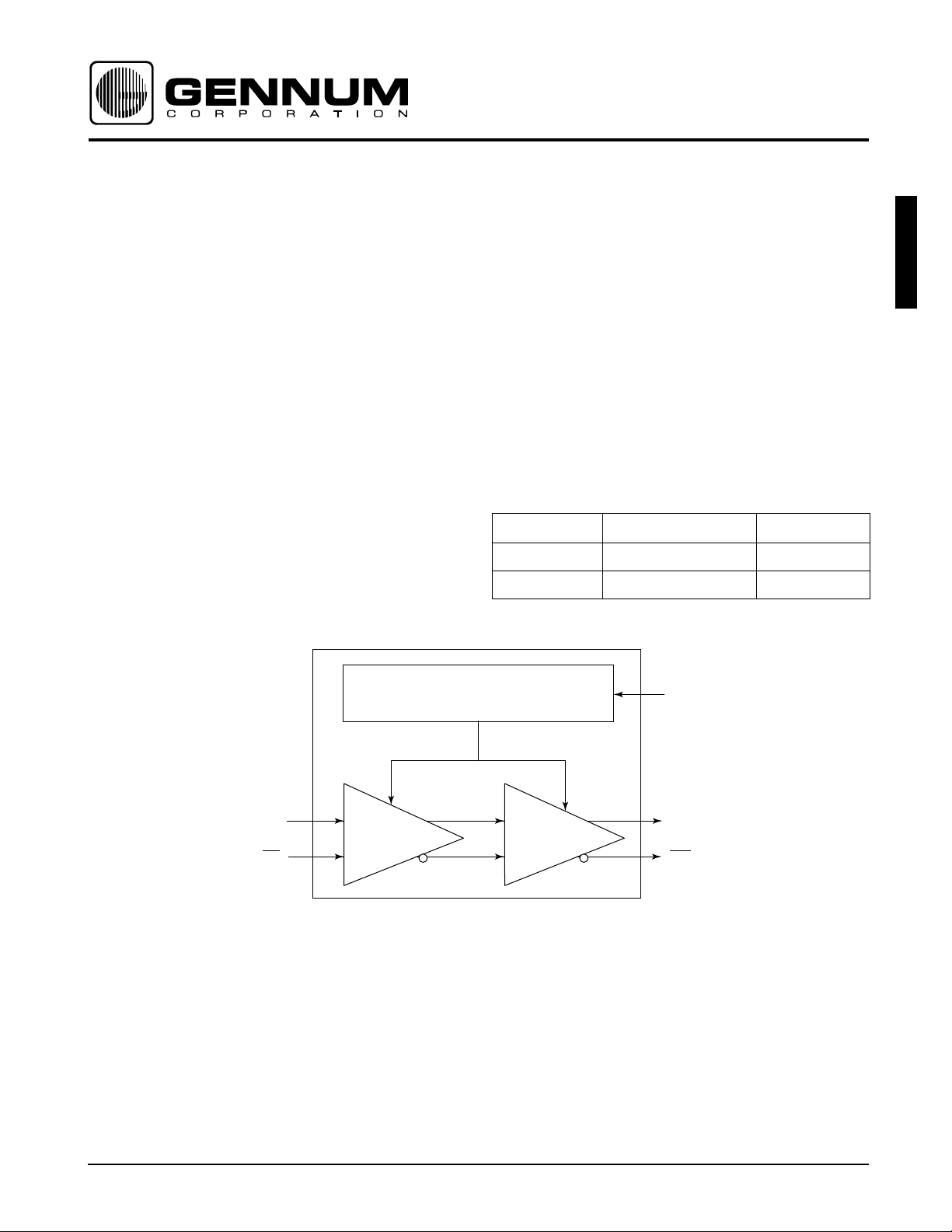
BANDGAP REFERENCE AND BIASING CIRCUIT
INPUT
DIFFERENTIAL
PAIR
PATENT PENDING
OUTPUT STAGE &
CONTROL
R
SET
SDO
SDO
BLOCK DIAGRAM
Revision Date: March 2000 Document No. 522 - 02 - 03
GENNUM CORPORATION P.O. Box 489, Stn. A, Burlington, Ontario, Canada L7R 3Y3
Tel. +1 (905) 632-2996 Fax. +1 (905) 632-5946 E-mail: info@gennum.com
www.gennum.com

ABSOLUTE MAXIMUM RATINGS
TA = 25°C unless otherwise indicated
PARAMETER VALUE
Supply Voltage 5.5V
Input Voltage Range (any input) -0.3 to (V
+0.3)V
CC
Operating Temperature Range 0°C to 70°C
Storage Temperature -65°C to 150°C
Power Dissipation 300mW
Lead Temperature (soldering, 10 sec) 260°C
GS1508
Input ESD Voltage 2000V
DC ELECTRICAL CHARACTERISTICS
VCC = 5V, TA = 0°C to 70°C unless otherwise shown.
Specifications assume 800mV output amplitude level settings into end terminated 75Ω transmission lines. Data Rate = 1485Mb/s unless otherwise shown.
PARAMETER CONDITIONS SYMBOL MIN TYP MAX UNITS NOTES
Supply Voltage V
System Power
Consumption
Driving two
75Ω cables
Supply Current
Common Mode Input
V
CC
P
D
I
S
CM,IN
4.75 5.00 5.25 V 1
- 215 265 mW 1
-4354mA 1
2.5+(V
)-V
DIFF/2
-(V
CC
)V 2
DIFF/2
Voltage Range
Common Mode Output
V
CM,OUT
-V
CC-VOUT
-V 2
Voltage Range
AC ELECTRICAL CHARACTERISTICS
VCC = 5V, TA = 0°C to 70°C unless otherwise shown.
Specifications assume 800mV output amplitude levels into end terminated 75Ω transmission lines. Data Rate = 1485Mb/s unless otherwise shown.
PARAMETER CONDITIONS SYMBOL MIN TYP MAX UNITS NOTES
Serial Digital Rate DC 1485 - Mb/s 1
Additive Jitter 1485Mb/s - 5 - ps
Differential Input V
Differential Output V
DIFF
OUT
150 - 800 mV diff p-p 2
750 800 850 mV p-p 1
RMS
13
TEST
LEVEL
TEST
LEVEL
Output Rise/Fall Times (20% - 80%) t
Mismatch in Output Rise/Fall
, t
R
F
- 120 250 ps 2 1
-1530ps 4
Times
Overshoot - 1 8 % 4
Duty Cycle Distortion - 15 30 ps 1
Output Return Loss 5MHz to 1485MHz - 17 - dB 2 4
NOTES:
1. RMS additive jitter measured using Pseudo Random bit sequence (2
2. Measured with Gennum Evaluation Board (EB1508).
23
- 1).
TEST LEVELS:
1. 100% tested at 25°C.
2. Guaranteed by design.
3. Correlated Value.
4. Tested with EB1508
2
522 - 02 - 03

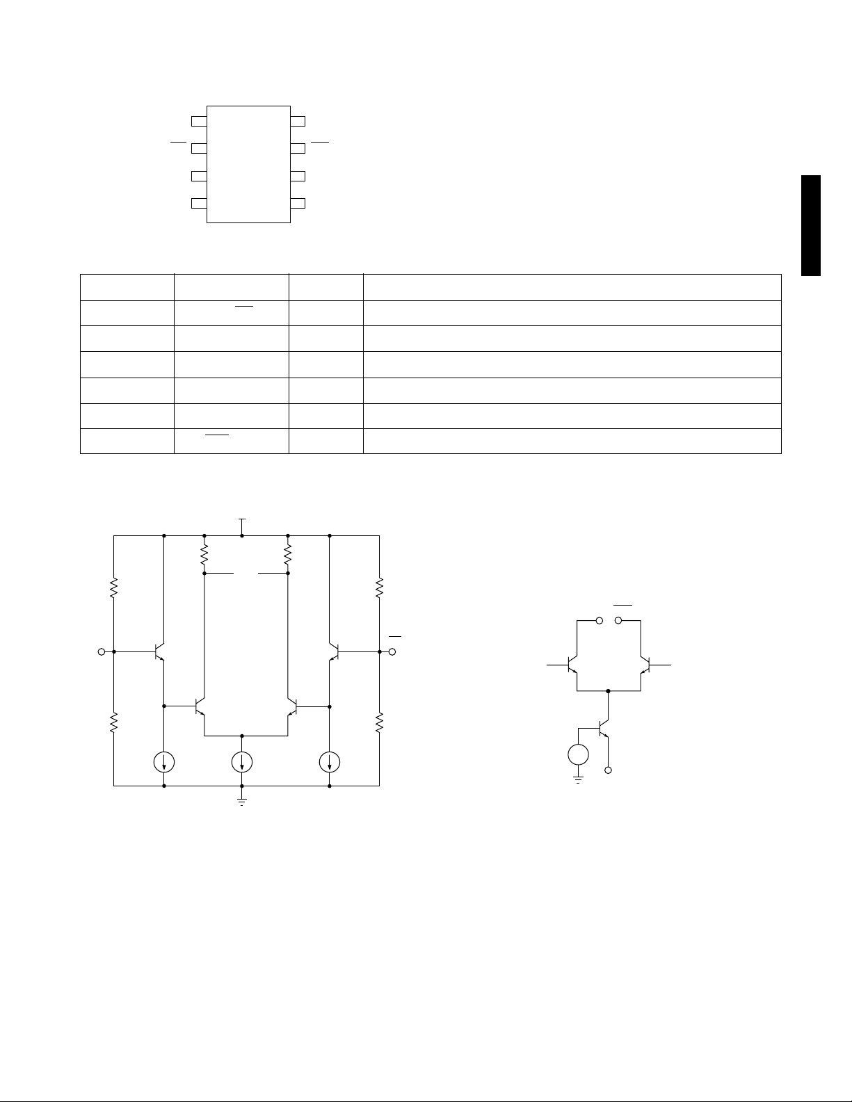
PIN CONNECTIONS
R
SET
SDO
SDO
+
-
TOP
8
SDO
7
SDO
6
GND
5
V
CC
R
SDI
SDI
V
SET
EE
1
2
GS1508
3
VIEW
4
PIN DESCRIPTIONS
NUMBER SYMBOL TYPE DESCRIPTION
1, 2 SDI, SDI
3V
4R
5V
EE
SET
CC
I Serial data inputs (non-inverting and inverting).
P Most negative supply voltage.
I Output amplitude control resistor.
P Most positive supply voltage.
6 GND P Not connected internally. Connect to Ground. Used for isolation.
7, 8 SDO
, SDO O Serial data outputs (non-inverting and inverting).
INPUT / OUTPUT CIRCUITS
V
CC
GS1508
SDI
5k
SDI
20k
Fig. 1 (Pins 1 and 2) Fig. 2 (Pins 7 and 8)
3
522 - 02 - 03
 Loading...