FEATURES
• general purpose
• EEPROM non-volatile memory
• 8 programmable current sink (PCS) control outputs
• can be configured with 6 PCS outputs for hearing
instruments (two switchable, four non-switchable)
• status register
• data transmission error detection
• synchronization of GP521 internal clocks with program
unit clock
STANDARD PACKAGING
• Chip (129 x 112 mils)
Au Bump
DESCRIPTION
The GP521 is a general purpose controller/memory chip in-
tended for use with audio signal path circuits in programmable
hearing instruments.
The GP521 uses a flexible communication standard which
allows room for future growth in programmable functions for
hearing instruments. The communication with the program unit
is over a bi-directional serial data link. Error detection circuitry
is used to avoid undesired changes in programmed settings.
General Purpose
Controller / Memory Chip
for Hearing Instruments
GP521 - DATA SHEET
An information transfer dialogue consists of the address and
data for a register sent to the GP521 and the register contents
returned by the GP521. The function controlled by an output of
the GP521 is defined by the signal path circuit allowing current
controlled parameters. The relationship between the GP521
register addresses and the function on the signal path circuit
is defined by a data file in the programming unit. With this
format, any software developed for the GP521 can be used for
future generations of Gennum’s controller/memory circuits
and audio signal path circuits.
The GP521 uses EEPROM cells as the long term memory
element. These cells will retain the stored data when the power
supply is disconnected. Each EEPROM cell is combined with
a temporary (RAM) memory cell which makes it possible to
evaluate various control settings prior to saving them in the
long term EEPROM memory.
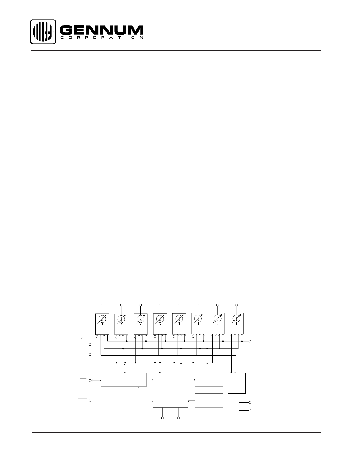
The GP521 controls the audio signal path circuit using eight
Programmable Current Sinks (PCS). Each PCS has 16 programmable settings. The circuit can be configured for either 6
or 8 PCS outputs. When used with a single pole single throw
switch (SPST) under the 6 PCS configuration , it is possible to
design a hearing instrument with two programmed settings
(i.e. adjusting a low cut filter for either noisy or quiet background environments). The 8 output configuration may be
used for circuits that require more programmable but nonswitchable settings. An external reference current is used for
the PCS’s so that the PCS outputs can track with the currents
in the audio signal path circuit.
BLOCK DIAGRAM
CONTROL OUTPUTS
O3
CONTROL OUTPUTS
I
O4
4 BIT
EEPROM
DAC
CONTROLLER TIMING
SW OFF
I
O5
4 BIT
EEPROM
DAC
OS1
I
O6
15 13 12 11
4 BIT
EEPROM
DAC
64
EEPROM
EEPROM
VOLTAGE
MULTIPLIER
OSCILLATOR
I
O7
4 BIT
DAC
STATUS &
OPERATION
REGISTER
I
4 BIT
EEPROM
DAC
O8
REFERENCE
CURRENT
17
I
I
R
R
16
N/C
14
N/C
GND
DATA
CLOCK
I
O1
4 BIT
EEPROM
DAC
V
CC
3
5
2
1
I
O2
10 9 8 7
4 BIT
EEPROM
DAC
SERIAL TO PARELLEL
CONVERSION
DATA ERROR CHECKING
I
4 BIT
EEPROM
DAC
Revision Date: May 1998
GENNUM CORPORATION P.O. Box 489, Stn. A, Burlington, Ontario, Canada L7R 3Y3 tel. +1 (905) 632-2996
Web Site: www.gennum.com E-mail: hipinfo@gennum.com
Document No. 510 - 79 - 06

ABSOLUTE MAXIMUM RATINGS
PARAMETER VALUE / UNITS
Supply Voltage 3 V DC
Min. voltage any pin GND - 200 mV
Max. voltage any pin VCC + 200 mV
Operating temperature 0 to 50 oC
CAUTION
CLASS 1 ESD SENSITIVITY
CLOCK
1
2
3
4
GND
5
6
I
7
I
8
DATA
V
CC
SWOFF
OS1
O4
O3
GP521
I
17
R
16
NC
I
15
O5
NC
14
I
13
O6
12
I
O7
11
I
O8
I
10
O1
I
9
O2
Fig. 1 Chip Pad Diagram
ELECTRICAL CHARACTERISTICS
Current into IC considered positive.
Conditions: Temperature = 25
o
C, I
= 4 µA, V
R
= 1.3 V
cc
PARAMETER SYMBOL CONDITIONS MIN. TYP. MAX UNITS
Supply Voltage V
Supply Current: I
cc
CC
Normal operation mode - - 25 µA
Program mode - - 1 mA
EEPROM read / write cycles 1000 - - cycles
- 1.3 3 V
Low Input Voltage "low" V
High Input Voltage "high" V
Clock Rate ƒ
L
H
CL
V
- - 200 mV
- 0.2 - - V
CC
- 6 50 kHz
PROGRAMMABLE CURRENT SINKS
Reference current I
PCS Bias Voltage V
R
PCS
Number of Settings N/A 16 N/A
Output Current for set "15" I
o15
DAC set to 15 V
= 0.5 V (note 2) 6.81 7.5 8.25 µA
PCS
Linearity Error η DAC set for 1,2,4,8 (note 1, 2) N/A ±10% N/A
Output Current offset "0" I
Output Leakage Current I
Early Voltage = V
1
OFFS
L
a
DAC set to 0 (note 1, 2) - 0 - nA
DAC set to 0 V
= 0.5 V (note 1, 2) - 0 - nA
PCS
DAC set to 15 (note 1, 2)
Set V
= 0.5V and - 37 - V
PCS
Channel length modulation
V
= 0.7V (S9 = b)
PCS
- - 14 µA
400 500 - mV
-
510 - 79 - 06
All switches remain as shown in Test Circuit unless otherwise stated in condition columns.
NOTES:
1. Refer to the definition section
2. Measurements performed for all DAC's separately (SWS 1 to 8 closed sequentially).
2

CLOCK
1.3 V
-
18 K
+
V = 1.3 V
-
B
+
1.3 V
DATA
V
REF
-
18 K
+
DATA CLOCK OSI SWOFF V GND
I01I02I03I
CC
I
04
05
=0.65V
SWS 1 2 3 4 5 6 7 8
DATA RET
+
-
+
1.3 V
22 K
27 K
22 K
All resistors in ohms, all capacitors
in µF unless otherwise stated
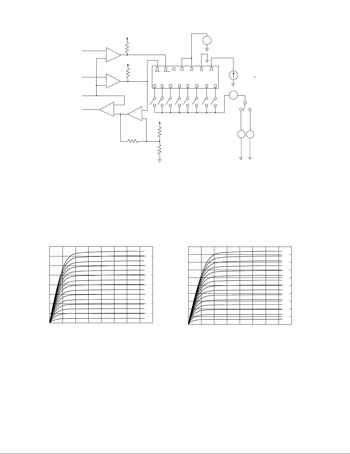
Fig. 2 Digital Test Circuit
GP521 DIGITAL TESTING
The GP521 is tested for digital functionality via a series of
For a summary of the actual testing refer to Document No. 520-35
reads
I
06
and
I
07
writes
R
I08I
I
R
A
I
O
a
+
0.5 V
-
to the GP521.
= 4 A
u
S9
b
+
-
0.7 V
8
7
6
5
4
3
PCS CURRENT (µA)
2
1
0
15
14
13
12
11
10
9
8
7
6
5
4
3
2
1
0 0.1 0.2 0.3 0.4 0.5 0.6 0.7 0.8
PCS VOLTAGE (V)
Fig. 3 PCS Current (Sink) vs PCS Voltage at DAC
Setting 0 to 15, IR = 4µA
10
9
8
7
6
5
4
PCS CURRENT (µA)
3
2
1
0
0 0.1 0.2 0.3 0.4 0.5 0.6 0.7 0.8
PCS VOLTAGE(V)
Fig. 4 PCS Current (Sink) vs PCS Voltage
I
= 0 to 7.5µA (step 0.5µA) DAC set at 10
R
7.5
7
6.5
6
5.5
5
4.5
4
3.5
3
2.5
2
1.5
1
0.5
3
510 - 79 - 06
 Loading...