Gennum Corporation GO1515-CTA Datasheet

FEATURES
• generates 1.485GHz or 1.485/1.001GHz signal for
HD-LINX™ ICs
• low current consumption
•50Ω output impedance
• operates from a single 5V supply
• 8 pin tape on reel
APPLICATIONS
VCO for the following HD-LINX™ ICs: GS1515, GS1522,
GS1540, GS1545.
ORDERING INFORMATION
PART NUMBER PACKAGE TEMPERATURE
GO1515 - CTA 8 pin tape on reel 0°C to 70°C
™
HD-LINX
GO1515
Voltage Controlled Oscillator
DATA SHEET
DESCRIPTION
The GO1515 is a self contained, miniature Voltage
Controlled Oscillator (VCO) that is used in conjunction with
Gennum’s HD-LINX™ ICs. It produces a clean 1.485GHz
reference clock signal for such devices as the GS1515
HDTV Reclocker and other HD-LINX™ devices. The control
voltage range is from 3.10 volts to 4.65 volts and is derived
from the on-chip PLLs. The GO1515 frequency can be
pulled approximately 16MHz for every one volt of control.
The output level is approximately 1.0dBm with low spurious
and noise content. It is designed to drive 50Ω strip lines.
The GO1515 VCO is used with the following HD-LINX™ ICs;
GS1515, GS1522, GS1540, GS1545 and is ordered as a
separate item. The VCO requires a single 5V supply and
draws a maximum of 15mA of current. It is packaged in a
miniature 8-pin proprietary surface mount package and
operates over the normal commercial temperature range of
0°C to +70°C.
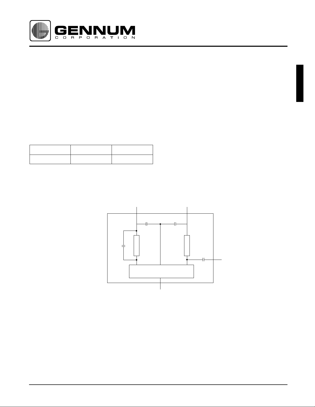
GO1515
3.3pF
V
CTR
OSCILLATOR CIRCUIT
GND
BLOCK DIAGRAM
V
CC
1000pF47pF
STRIPLINESTRIPLINE
2pF
OUT
Revision Date: March 2000 Document No. 522 - 40 - 02
GENNUM CORPORATION P.O. Box 489, Stn. A, Burlington, Ontario, Canada L7R 3Y3
Tel. +1 (905) 632-2996 Fax. +1 (905) 632-5946 E-mail: info@gennum.com
www.gennum.com

ELECTRICAL CHARACTERISTICS
VS = 5.0V ±0.25V, Temperature = 0°C to 70°C unless otherwise specified.
PARAMETER SYMBOL CONDITIONS MIN TYP MAX UNITS
Supply Voltage V
Supply Current
Control Voltage Range V
Control Voltage Sensitivity df/dV 11 16 21 MHz/V
GO1515
Operating Frequency
Range
Output Signal Level V
Signal to Noise Ratio S/N Signal Level: 1kHz ±8kHz
Carrier to Noise Ratio C/N 25kHz Separation, 1kHz Bandwidth 74 - - dBc
Pushing Figure V
Pulling Figure VSWR = 2.0 for all phase, ref: 50
Temperature Stability T
Spurious Response ---10dBc
Output Impedance Z
PIN CONNECTIONS
ƒ
COEF
CC
Ι
S
CTR
VCO
OUT
O
4.75 5.0 5.25 V
--15mA
+3.1 - +4.65 V
1483.5 - 1485.5 MHz
-2 1 +4 dBm
40 - - dB
Deviation = 0.3~3.0kHz
= 5.0V ±0.25V, ref: VS = 5.0V - ±500 - kHz
S
Ω
- ±1000 - kHz
0°C to 70°C, ref. = 25°C - - ±3 MHz
-50-
Ω
NC GND O/P
765
GO
8
4
GNDGND
1515
TOP VIEW
132
V
NOTE: Pin numbers are arbitrary.
There are no pin markings on the device itself
PIN DESCRIPTIONS
NUMBER SYMBOL TYPE DESCRIPTION
2, 4, 6, 8 GND - Most negative power supply connections.
1V
3V
CTR
CC
5 O/P O VCO signal output.
7 NC - No connection.
I Control voltage for the VCO.
- Most positive power supply connection.
CTR
GND V
CC
522 - 40 - 02
2
 Loading...