Gennum Corporation GM3008 Datasheet

Stand Alone
Class B Hybrid
GM3008 - HYB DATA SHEET
FEATURES
• up to 80 dB of electrical gain
• dedicated preamp for a telecoil
• direct coupling of a telecoil to preamp
• low input referred noise
• on chip voltage regulator
• capable of driving low impedance receivers
STANDARD PACKAGING
• Hybrid typical dimensions
0.250 in x 0.150 in x 0.115 in
(6.35 mm x 3.81 mm x 2.92 mm)
DESCRIPTION
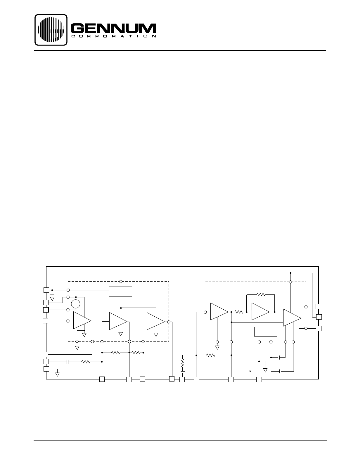
The GM3008 hybrid consists of two of Gennum's proprietary
integrated circuits, the GP537 preamplifier and the GS551
class B output driver. Such a configuration provides up to
80 dB (typ) of electrical gain. Low total harmonic distortion
and input noise make this circuit well suited for high power
applications. Various additional pads have been provided
to allow for maximum flexibility of system performance.
The GP537 contains two low noise inverting preamplifiers
with an open loop voltage gain of typically 50 dB, a telecoil
preamplifier with its own reference voltage which enables
for direct coupling of the telecoil and a voltage regulator
with typically 74 dB of supply rejection capable of working
with a supply voltage down to 1.1 volts. This chip also
enables the user to disconnect the telecoil preamplifier
when it is not required, thereby saving approximately
85 µA of current.
The GS551 class B amplifier contains three basic blocks,
a low noise inverting preamplifier, a unity gain phase
splitter and a fixed gain class B output stage.
V
REG
11
C1
V
BT
T
REF
T
IN
T
OUT
INPUT
MGND
Revision Date: May 1998
3µ3
16
15
14
13
10
12
All resistors in ohms, all capacitors
in farads unless otherwise stated.
C2
47n
GENNUM CORPORATION P.O. Box 489, Stn. A, Burlington, Ontario, Canada L7R 3Y3 tel. +1 (905) 632-2996
5
B
OUT
GM3008
R4 15k
C3 47n
8
9
C
GS551
5
-
C
2
4
R5
60k
65
C
F
IN
C
OUT
-
D
REFERENCE
VOLTAGE
9
1
PGND
6
1
4
OUT 1
3
2
V
CC
OUT 2
E
10
7
C4
47n
C5
47n
3
8
3
2
4
REGULATOR
GP537
+
-
1
11
-
T
9
R1
18k2
-
A
8
10
R2
105k
17
A
IN
18
A
OUT
7
R3
20k
-
B
6
7
B
IN
FUNCTIONAL BLOCK DIAGRAM
Document No. 520 - 70 - 05
Web Site: www.gennum.com E-mail: hipinfo@gennum.com

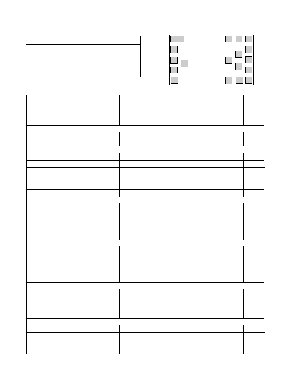
ABSOLUTE MAXIMUM RATINGS
PAD CONNECTION
PARAMETER VALUE / UNITS
Supply Voltage 3 VDC
Power Dissipation 25 mW
Operating Temperature Range -10° C to 40° C
Storage Temperature Range -20° C to 70° C
1
2
16
3
6
18
17
4
8
5
7
ELECTRICAL CHARACTERISTICS
Conditions: Frequency = 1 kHz, Temperature = 25°C, Supply Voltage VCC = 1.3 V Notes:1. All capacitors on hybrid ±20%, all printed on resistors ±5%
PARAMETER SYMBOL CONDITIONS MIN TYP MAX UNITS
Amplifier Current I
Telecoil Current I
Transducer Current I
AMP
TCOIL
TRANS
REGULATOR
Regulator Voltage V
REG
Regulator Supply Rejection PSRR 60 74 - dB
T COIL
Bias Voltage V
Telecoil Offset Voltage V
Input Bias Current I
Output Voltage Swing - Low V
Maximum Sourcing Current I
Open Loop Voltage Gain A
BIAS
TOFF
BIAS
OL
SOURCE
VOL
STAGES A & B
Bias Voltage V
Input Bias Current I
Output Voltage Swing - Low V
Maximum Sourcing Current I
Open Loop Voltage Gain A
BIAS
BIAS
OL
SOURCE
VOL
STAGE C
Bias Voltage V
Input Bias Current I
Output Voltage Swing - Low V
Maximum Sourcing Current I
Open Loop Voltage Gain A
BIAS
BIAS
OL
SOURCE
VOL
STAGE D
Voltage Gain GAIN - 0 - dB
STAGE E
AC Voltage Gain GAIN - 28 - dB
Maximum Sourcing Current I
SOURCE
SYSTEM PERFORMANCE
System Voltage Gain S
Telecoil Gain T
GAIN
GAIN
Total Harmonic Distortion THD VIN = -60dB, RF = 39k - 3 5 %
Input Referred Noise IRN - 2.5 - µV
All parameters and switches remain as shown in the Test Circuit unless otherwise stated in CONDITIONS column.
520 - 70 - 05
S1 = Open 190 365 550 µA
40 85 130 µA
Quiescent Current VIN = 0 V 100 250 390 µA
0.88 0.93 0.98 V
Pads 13, 14 540 580 620 mV
V
P15
- V
P14
-10 0 10 mV
-25 0 25 nA
200 280 - mV
15 30 - µA
46 50 - dB
Pads 7, 9, 17, 18 540 580 620 mV
-25 0 25 nA
200 280 - mV
15 30 - µA
46 50 - dB
Pads 5, 6 540 580 620 mV
-0 -nA
- 280 - mV
-50 -µA
-50 -dB
- >35 - mA
VIN = -60 dBV, RF = 39k 56 60 64 dB
S2 = b; VIN = -60 dBV 16 18.5 20 dB
2
131415
12
11
10
9

V
IN
(0V AC)
GM3008
GS551
5
-
C
B
5
2
-
D
REFERENCE
VOLTAGE
4
9
6
1
E
10
7
3
8
1.3 VDC
4
3
I
AMP+ITCOIL
2
I
TRANS
V
OUT
390
C4
R4 15k
C3 47n
9
R5
60k
8
6
5
47n
C5
47n
1
C1
3µ3
3
2
+
-
1
11
-
T
10
9
11
S1
16
15
1µ
14
10k
1k
REGULATOR
-
A
8
4
R2
13
S2
b
a
C2
10
47n
12
All resistors in ohms, all capacitors
in farads unless otherwise stated.
R1
18k2
105k
17
GP537
-
7
6
R3
20k
7
18
RF=390k
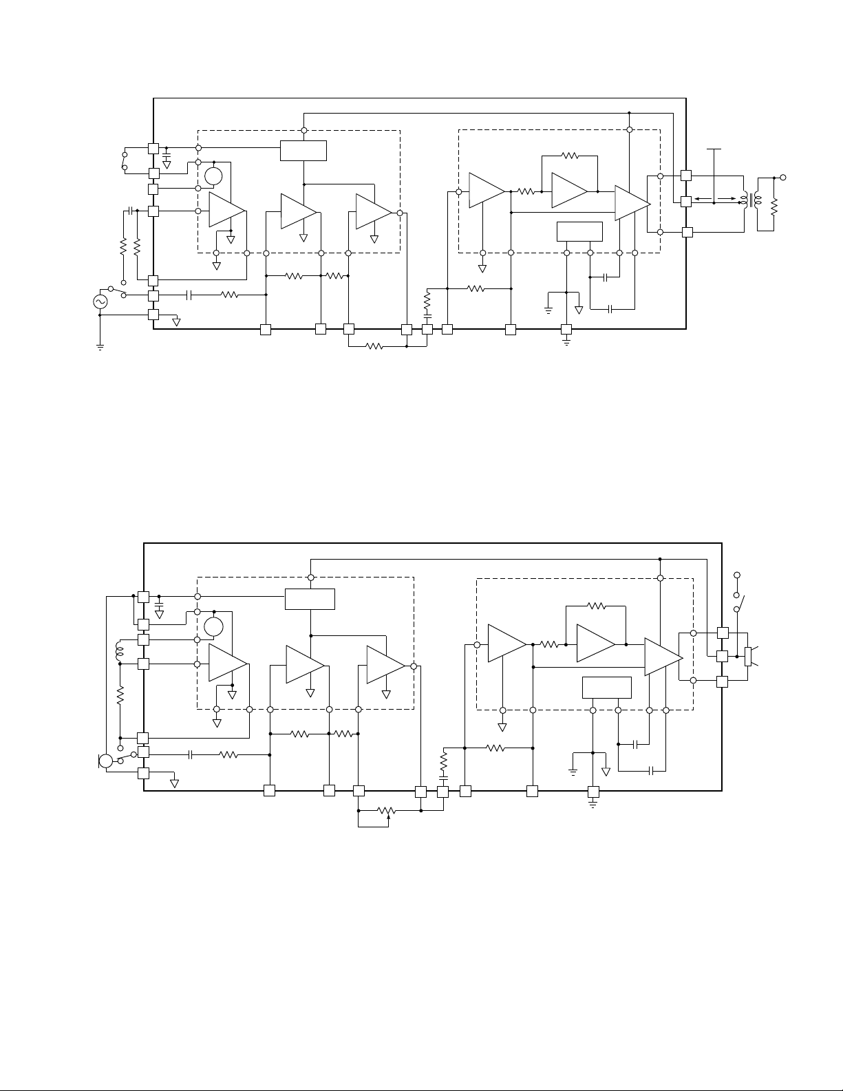
Fig. 1 Production Test Circuit
MIC
EK3024
C1
3µ3
3
2
+
-
1
11
-
11
16
15
14
10k
13
10
12
C2
47n
All resistors in ohms, all capacitors
in farads unless otherwise stated.
T
9
R1
18k2
GM3008
5
10
REGULATOR
-
A
8
R2
105k
4
GP537
-
B
7
6
R3
20k
R4 15k
C3 47n
7
17
18
390k
9
V.C.
Fig. 2 Typical Hearing Instrument Application
1.3VDC
GS551
5
-
C
2
4
-
D
REFERENCE
VOLTAGE
9
R5
60k
8
6
5
1
6
1
4
E
7
3
8
3
10
REC
2
CI2960
C4
47n
C5
47n
3
520 - 70 - 05
 Loading...