Gennum Corporation GH580 Datasheet

FEATURES DESCRIPTION
Adjustable Analog
Highpass Filter
GH580 - DATA SHEET
• 200 to 8 kHz adjustable corner frequency
• 12 dB/oct Butterworth filter
• low current drain (175 µA typical)
• two on chip 1 nF capacitors
• low noise and distortion
• 1.1 to 3.0 VDC operation
STANDARD PACKAGING
• 8 pin PLID
®
• Chip (66 x 61 mils)
The GH580 is a single, second order (12 dB/Oct) continuous
high pass filter with an adjustable corner frequency (ƒ
200 to 8 kHz. Adjustment of ƒ
is accomplished with a single
C
) from
C
100 kΩ potentiometer connected from pin 3 to ground.
The bias circuitry is operated from an on chip voltage regulator
providing good supply rejection down to 1.1 V.
The two integrated 1 nF capacitors have parasitic diodes
connected in parallel. This necessitates that the DC voltage
at pin 6 be greater that 400 mV and less than VB and that pins
8 and 7 be no greater than approximately 400 mV DC.
The GH580 has a dynamic range of approximately 80 dB.
V
B
4
Revision Date: January 2001
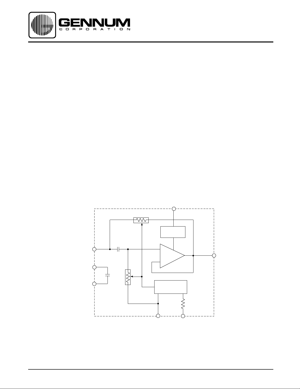
A IN
CP+
CP-
V
REG
8
6
7
+
1n
+
1n
1
GND
+
A
_
CONTROL
A OUT
5
3
R
CNT
BLOCK DIAGRAM
Document No. 520 - 50 - 05
GENNUM CORPORATION P.O. Box 489, Stn. A, Burlington, Ontario, Canada L7R 3Y3 tel. +1 (905) 632-2996
Web Site: www.gennum.com E-mail: hipinfo@gennum.com

ABSOLUTE MAXIMUM RATINGS
PIN CONNECTION
PARAMETER VALUE/UNITS
Supply Voltage 5 V DC
Power Dissipation 25 mW
Operating Temperature Range -10°C to +40° C
Storage Temperature Range -20°C to +70° C
V
RCNT
NC
GND
4
B
1
5
A OUT
CP+
CP-
8
A IN
CAUTION
CLASS 1 ESD SENSITIVITY
ELECTRICAL CHARACTERISTICS
Conditions: Frequency = 1 kHz, Temperature = 25°C, VB = 1.3V
PARAMETER SYMBOL CONDITIONS MIN TYP MAX UNITS
Amplifier Current I
Bias Voltage (Pin 6) V
Bias Voltage (Pin 8) V
Insertion Loss I
Output Noise O
AMP
P6
P8
LOSS
NOISE
SW1 to closed, VIN = 40 mVRMS - 1.7 2.0 dB
SW1 to closed, VIN = 0 mVRMS -57µV
NFB 200 Hz to 10 kHz at 12dB/oct
Distortion THD SW1 to closed, VIN = 50 mVRMS -15%
120 175 210 µA
- 100 - mV
- 350 - mV
Supply Rejection (Pin 4 to Pin 5) PSRR Note 1, Pin 4 to Pin 5 48 56 - dB
Corner Frequency ƒ
All parameters and switches remain as shown in Test Circuit unless otherwise stated in "Conditions" column
Notes: 1. V
2. F
modulated with 1kHz
B
= 1000 x 2A; A = (I
C
SW1
V
I
N
1kHz
LOSS -
20
8
6
7
C
LOG (VOUT
+
1n0
1n0
+
Note 2, R
/0.04))/12
= 10.27k 1300 1650 1900 Hz
CNT
V
=1.3VDC
B
I
AMP
4
V
REG
+
_
CONTROL
1
A
1.8K
3
R
CNT
100K
5
1µ0
R
V
L
OUT
=10K
520 - 50 - 05
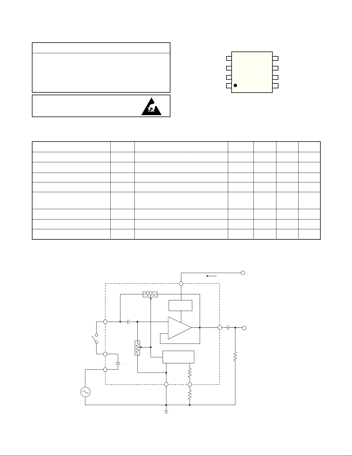
All resistors in ohms, all capacitors
in farads unless otherwise stated
Fig. 1 Test Circuit
2
 Loading...