TM
Multi
GEN
GF9105A
Component Digital Transcoder
DATA SHEET
FEATURES
• drop in replacement for the GF9105 with lower power
and increased functionality
• new mode for HVF output
• new mode for using low frequency clocks with nonmultiplex ed I/O data
• optimized HOST IF control signals for ensured shared
bus compatibility
• multiple format conversions from one device
4:2:2:4 <-> 4:4:4:4
4:2:2:4 <-> R/G/B/KEY
4:2:2:4 <-> Y/U/V/KEY
Y/U/V/KEY <-> R/G/B/KEY
4:4:4:4 <-> R/G/B/KEY
4:4:4:4 <-> Y/U/V/KEY
• ITU-R-601 compliant interpolation/decimation filters
• supports both single link 4:4:4:4 (SMPTE RP174) and
dual link 4:4:4:4 (SMPTE RP175) compliant I/O
• transparent conversions between Y/U/V and R/G/B
color spaces.
• fully programmable 3X3 Color Space Converter (CSC)
• 13 bit Color Space Converter coefficients
• 13 bit KEY Channel scaling coefficient
• multiplexed and non-multiplexed I/O data
• bi-directional I/O data ports with tri-stating
• parallel HOST IF for reading and writing multiplier
coefficients and device configuration words
• single +5V power supply.
ORDERING INFORMATION
PART NUMBER PACKAGE
GF9105ACQQ 160 Pin MQFP
DEVICE OVERVIEW
The GF9105A is a drop in replacement for the GF9105 with
lower power and increased functionality. This increased
functionality gives the user the option of having HVF output
signals and the option of using a low frequency clock when
operating with non-multiplexed input and output data. The
GF9105A is a flexible VDSP engine capable of performing a
variety of format conversions. The flexible architecture of
the GF9105A also allows the user to perform a wide range
of DSP functions that require a general 3X3 multiplier
structure and/or high performance 1:2 interpolation and 2:1
decimation filters. Device configuration is selected by
writing configuration words through an asynchronous
parallel interface (HOST IF).
The GF9105A accepts either multiplexed or nonmultiplexed input data and may produce either multiplexed
or non-multiplexed output data. External H, V and F inputs
allow for the insertion of TRS words into multiplexed output
data streams.
All interpolation and decimation filtering required for ITU-R601 compliant 4:2:2:4 <-> 4:4:4:4 sample rate conversions
has been integrated into the GF9105A. In addition, all input
and output offset adjustments required for transparent
conversions between the Y/U/V and R/G/B color spaces
have been included within the GF9105A.
The color space converter within the GF9105A has 13 bit
multiplier coefficients, has 13 bit output resolution,
maintains full precision throughout the 3X3 calculation and
has a true unity gain by-pass mode. Sufficient resolution is
maintained within the color space converter to ensure that
truly transparent Y/U/V <-> R/G/B conversions may be
achieved. A user programmable output clipper allows the
GF9105A to output a variety of word lengths to meet
specific system requirements.
The GF9105A is packaged in a 160 pin MQFP package,
operates from a single +5V supply.
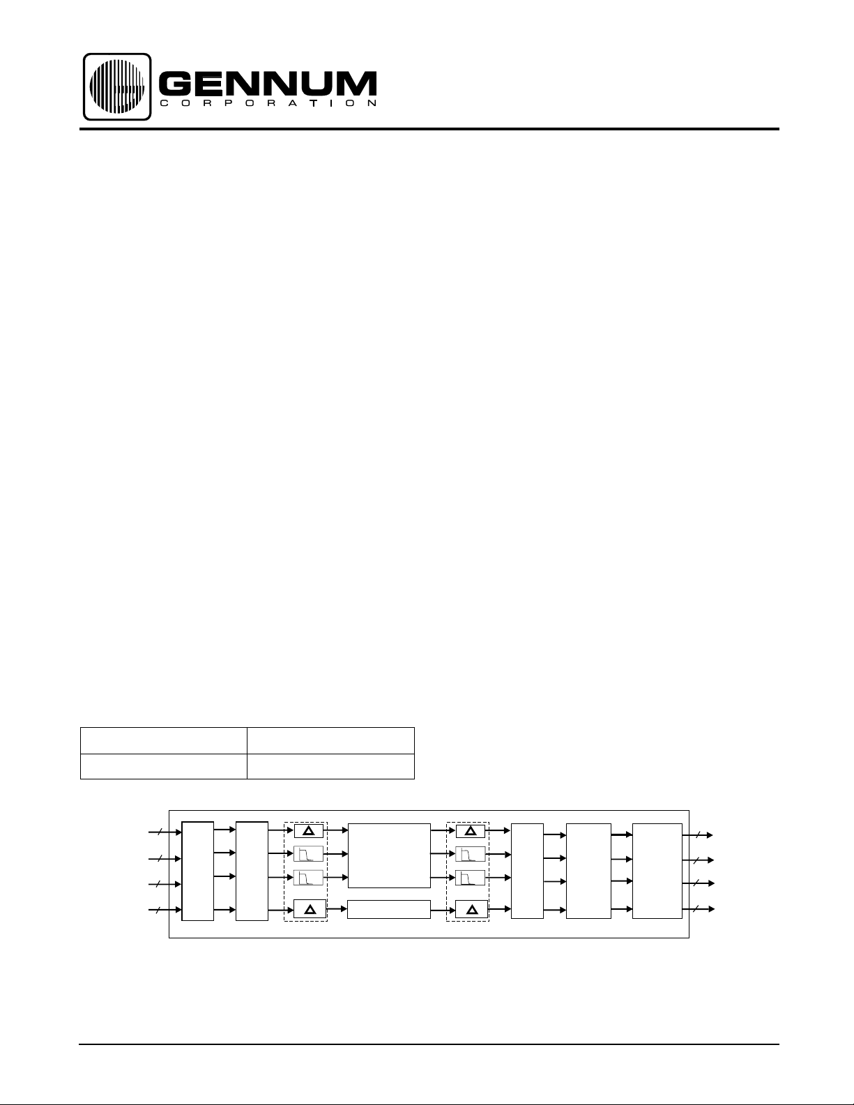
Y/G, CB/B, CR/R, KEY OR
Y/G, CB/B, CR/R, OR Y/G
XX OR CB/B
XX OR CR/R
KEY, CB/B, CR/R OR KEY
13
13
13
11
Y/G Y/G Y/G Y/G Y/G
KEY
INT
CB/B
INT
CR/R
KEY
DEMUX
4:4:4:4
OR
4:2:2:4
CB/B
CR/R
KEY
H_BLANK
AND
INPUT
OFFSET
ADJUST
CB/B
CR/R
3 X 3
MATRIX
MULTIPLIER
KEY SCALER
CB/B
CR/R
KEY
DEC
DEC
CB/B
CR/R
KEY
Y/G Y/G
OUTPUT
CB/B
OFFSET
ADJUST
CR/R
KEY KEY
OUTPUT
CLIP
CB/B
CR/R
OUTPUT
MULTIPLEXER
13
Y/G, CB/B, CR/R, KEY OR
Y/G, CB/B, CR/R, OR Y/G
13
CB/B OR XX
13
CR/R OR XX
11
KEY OR KEY, CB/B, CR/R
GENERAL FUNCTIONALITY OF GF9105A CORE
Revision Date: March 2000 Document No. 521 - 88 - 03
GENNUM CORPORATION P.O. Box 489, Stn. A, Burlington, Ontario, Canada L7R 3Y3
Tel. +1 (905) 632-2996 Fax. +1 (905) 632-5946 E-mail: info@gennum.com
www.gennum.com
PIN DESCRIPTION
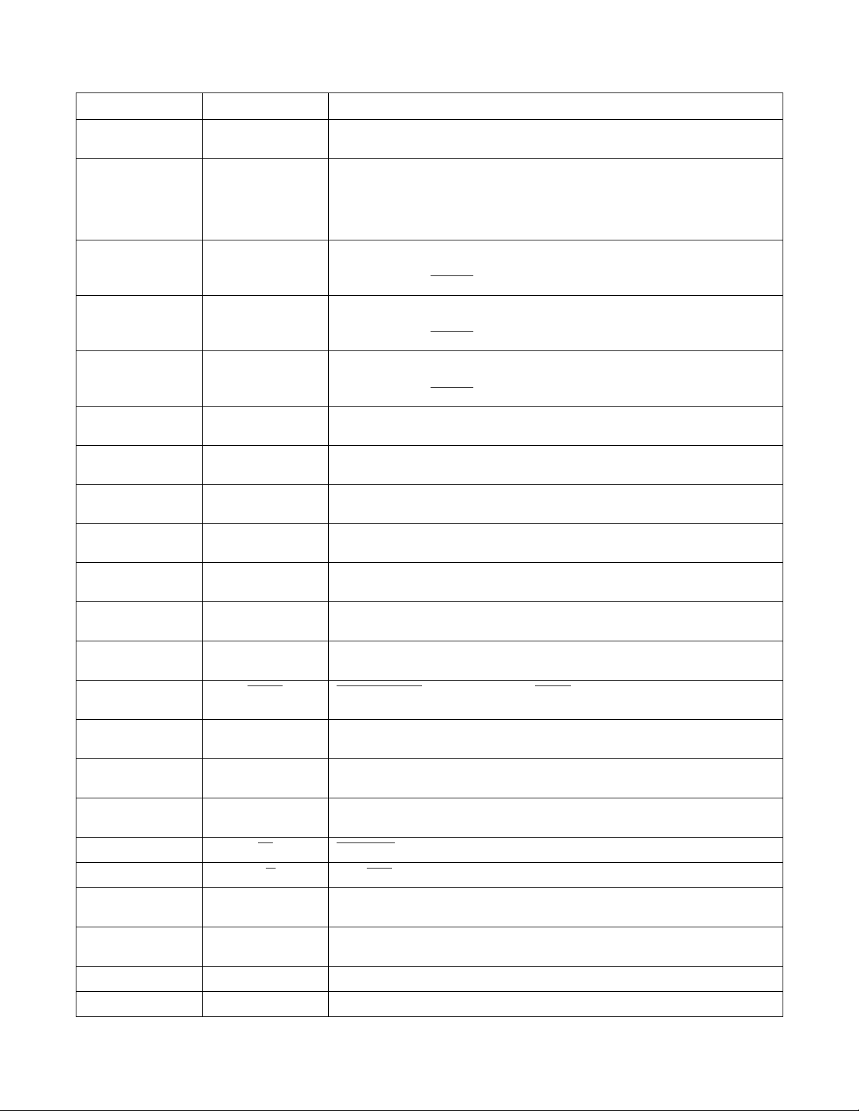
PIN NO. SYMBOL DESCRIPTION
11, 20, 51, 60, 80,
101, 121, 141, 150
4, 7, 10, 14, 21, 43,
52, 61, 63, 72, 81, 88,
96, 100, 105, 113,
120, 129, 138, 140,
149, 158
147, 148, 151-157,
P1
159, 160, 1, 2
131-137, 139, 142-
P2
146
115-119, 122-128,
P3
130
102-104, 106-112,
P4
114
54, 53, 50-44, 42-39 P5
70-64, 62, 59-55 P6
86-82, 79-73, 71 P7
99-97, 95-89, 87 P8
V
DD
+5 V ±5% power supply.
GND Ground.
12..0
12..0
12..0
10..0
12..0
12..0
12..0
10..0
Data Port No. 1: Depending on device configuration, P1
an output data port. Note: When HVF output is enabled H is always presented on P1
of the state of INPUT/
Data Port No. 2: Depending on device configuration, P2
an output data port. Note: When HVF output is enabled V is always presented on P2
of the state of INPUT/
Data Port No. 3: Depending on device configuration, P3
an output data port. Note: When HVF output is enabled F is always presented on P3
of the state of INPUT/
Data Port No. 4: Depending on device configuration, P4
an output data port.
Data Port No. 5: Depending on device configuration, P5
an output data port.
Data Port No. 6: Depending on device configuration, P6
an output data port.
Data Port No. 7: Depending on device configuration, P7
an output data port.
Data Port No. 8: Depending on device configuration, P8
an output data port.
OUTPUT
OUTPUT
OUTPUT
may operate as an input data port or
12..0
.
may operate as an input data port or
12..0
.
may operate as an input data port or
12..0
.
may operate as an input data port or
10..0
may operate as an input data port or
12..0
may operate as an input data port or
12..0
may operate as an input data port or
12..0
may operate as an input data port or
10..0
regardless
12
regardless
12
regardless
12
22 SYNC_CB Synchronization: Control signal input. SYNC_CB is used to synchronize the GF9105A to
the incoming data stream.
24 H_BLANK Horizontal Blanking: Control signal input. H_BLANK is used to replace portions of the
input data with a user selectable set of blanking levels.
25 DP_EN
Data Port Enable: Control signal input. DP_EN is used to enable and disable data
ports P1 - P8.
17 H Horizontal: Control signal input. H identifies the horizontal blanking interval for the
output multiplexer.
16 V Vertical: Control signal input. V identifies the vertical blanking interval for the output
multiplexer.
18 F Field: Control signal input. F is used to identify field information for the output
multiplexer.
26 CS
23 R/W
27-31 ADDR
3, 5, 6, 8, 9, 12, 13,
COEFF_PORT
15
4..0
7..0
Chip Select: Host interface control signal input.
Read/Write: Host interface control signal input.
Coefficient Address: Input port to identify which GF9105A device address shall be
written to/read from.
Coefficient Port: Host interface bi-directional data port for Color Space Converter
coefficients, KEY scaler coefficient and device configuration words.
19 CLK System Clock: All timing information is relative to the rising edge of CLK.
32 TCK JTAG Test Clock Input: Independent clock signal for JTAG.
521 - 88 - 03
2
PIN DESCRIPTION
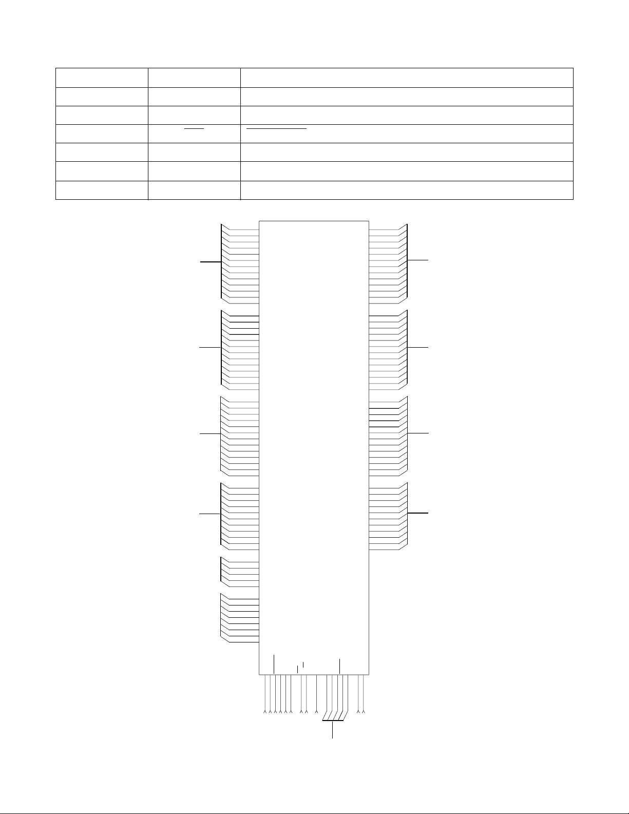
PIN NO. SYMBOL DESCRIPTION
33 TDI JTAG Test Data Input: Serial input for JTAG test data.
34 TMS JTAG Test Mode Select: Serial input for selecting JTAG test mode.
35 TRST
JTAG Test Reset: Connect to GND for normal operation.
36 TDO JTAG Test Data Output: Serial output for JTAG test data.
37 TN_IN Connect to V
DD
.
38 PTO No Connect.
147
P112/H
P1
P1
P1
P1
P1
P1
P1
P1
P1
P1
1
P1
2
P1
P212/V
P2
P2
P2
P2
P2
P2
P2
P2
P2
P2
P2
P2
P312/F
P3
P3
P3
P3
P3
P3
P3
P3
P3
P3
P3
P3
P4
P4
P4
P4
P4
P4
P4
P4
P4
P4
P4
ADDR
ADDR
ADDR
ADDR
ADDR
3
COEFF_PORT
5
COEFF_PORT
6
COEFF_PORT
8
COEFF_PORT
9
COEFF_PORT
COEFF_PORT
COEFF_PORT
COEFF_PORT
11
10
9
8
7
6
5
4
3
2
1
0
11
10
9
8
7
6
5
4
3
2
1
0
11
10
9
8
7
6
5
4
3
2
1
0
10
9
8
7
6
5
4
3
2
1
0
OUT
OUT
OUT
4
3
2
1
0
GF9105A
7
6
5
4
3
2
1
0
148
151
152
P1
12..0
P2
12..0
P3
12..0
P4
10..0
153
154
155
156
157
159
160
131
132
133
134
135
136
137
139
142
143
144
145
146
115
116
117
118
119
122
123
124
125
126
127
128
130
102
103
104
106
107
108
109
110
111
112
114
27
28
29
30
31
12
13
15
54
P5
12
53
P5
11
50
P5
10
49
P5
9
48
P5
8
47
P5
7
46
P5
6
45
P5
5
44
P5
4
42
P5
3
41
P5
2
40
P5
1
39
P5
0
70
P6
12
69
P6
11
68
P6
10
67
P6
9
66
P6
8
65
P6
7
64
P6
6
62
P6
5
59
P6
4
58
P6
3
57
P6
2
56
P6
1
55
P6
0
86
P7
12
85
P7
11
84
P7
10
83
P7
9
82
P7
8
79
P7
7
78
P7
6
77
P7
5
76
P7
4
75
P7
3
74
P7
2
73
P7
1
71
P7
0
99
P8
10
98
P8
9
97
P8
8
95
P8
7
94
P8
6
93
P8
5
92
P8
4
91
P8
3
90
P8
2
89
P8
1
87
P8
0
P5
12..0
P6
12..0
P7
12..0
P8
10..0
SYNC_CB
H_BLANK
DP_ENHVFCS
R/W
CLK
TCK
TDI
TMS
TRST
TDO
TN_IN
PTO
222425171618262319323334353637
JTAG
38
DD
N.C
V
Fig. 1 GF9105A Data Pin Designations
3
521 - 88 - 03
P212/V
T
P112/H
OU
/F
7
COEFF
116 115 114 113 112 111 110 109 108 107 106 105 104 103 102 101 100120 119 118 117
GND
6
COEFF
12
P40GND
P41P42P43P44P45P46P47GND
5
4
3
GND
COEFF
COEFF
GND
COEFF
DD
V
1
COEFF2COEFF
GND
0
COEFF
P48P49P410VDDGND
GF9105A
TOP VIEW
F
V
H
CLK
P810P89P88GND
P87P86P85P84P83P82P81GND
99 98 97 96 95 94 93 92 91 90 89 88 87 86 85 84 83 82 81
DP_EN
HBLANK
4
CS
ADDR
DD
V
R/W
GND
SYNC_CB
0
ADDR3ADDR2ADDR1ADDR
TCK
GND
P38P39P310P311P3
V
121
DD
P3
122
7
P3
123
6
P3
124
5
P3
125
4
P3
126
3
P3
127
2
P3
128
1
GND
129
P3
130
0
131
OUT
P2
132
11
P2
133
10
P2
134
9
P2
135
8
P2
136
7
P2
137
6
GND
138
P2
139
5
GND
140
V
141
DD
P2
142
4
P2
143
3
P2
144
2
P2
145
1
P2
146
0
147
OUT
P1
148
11
GND
149
V
150
DD
P1
151
10
P1
152
9
P1
153
8
P1
154
7
P1
155
6
P1
156
5
P1
157
4
GND
158
P1
159
3
P1
160
2
1 2 3 4 5 6 7 8 9 10 11 12 13 14 15 16 17 18 19 20 21 22 23 24 25 26 27 28 29 30 31 32 33 34 35 36 37 38 39 40
0
P11P1
P80P712P711P710P79P78GND
TDI
TMS
TRST
TDO
TN_IN
PT0
P5
0P51
80
V
DD
79
P7
7
78
P7
6
77
P7
5
76
P7
4
75
P7
3
74
P7
2
73
P7
1
72
GND
71
P7
0
70
P6
12
69
P6
11
68
P6
10
67
P6
9
66
P6
8
65
P6
7
64
P6
6
63
GND
62
P6
5
61
GND
60
V
DD
59
P6
4
58
P6
3
57
P6
2
56
P6
1
55
P6
0
54
P5
12
53
P5
11
52
GND
51
V
DD
50
P5
10
49
P5
9
48
P5
8
47
P5
7
46
P5
6
45
P5
5
44
P5
4
43
GND
42
P5
3
41
P5
2
521 - 88 - 03
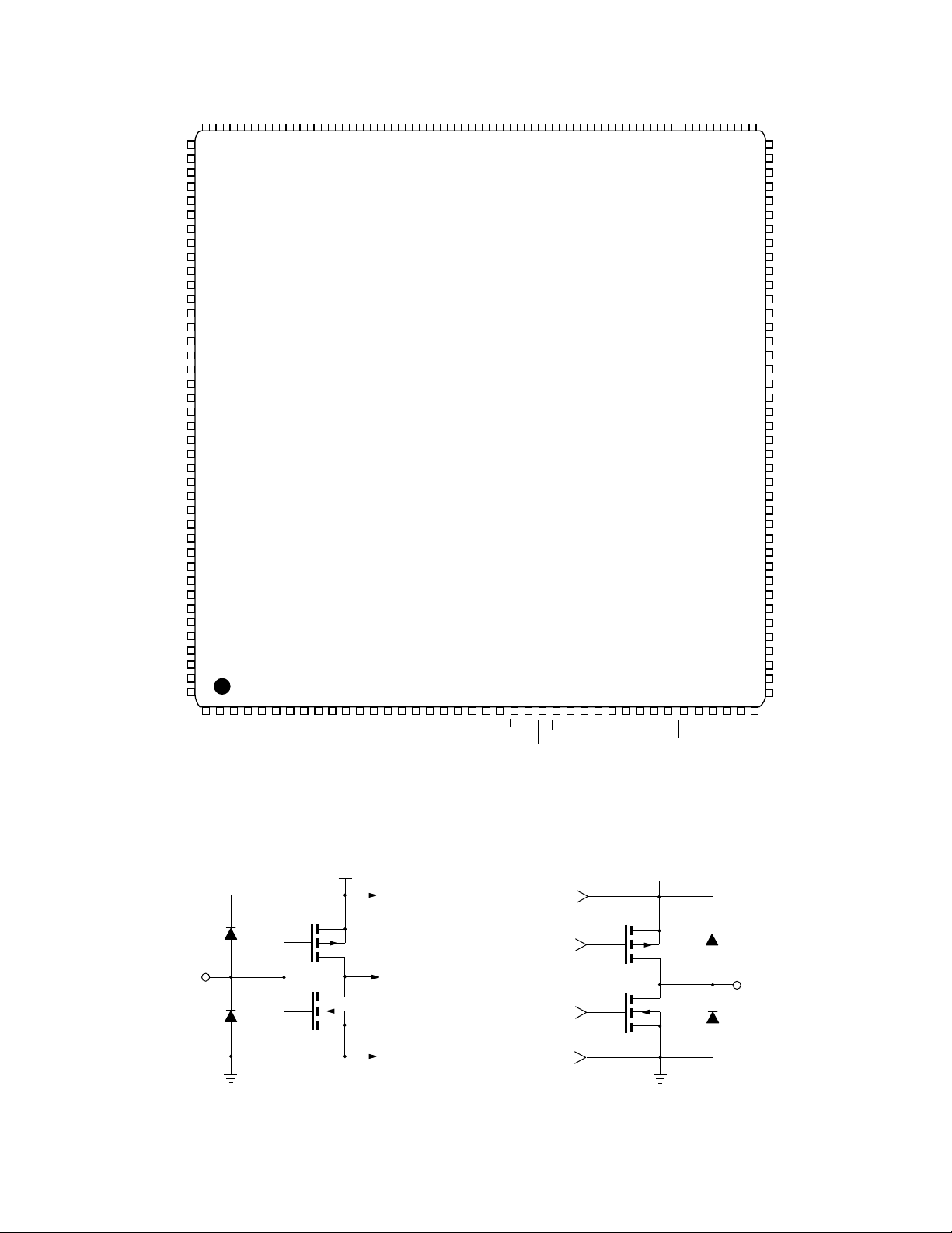
Fig. 2 GF9105A Pin Connections
n substrate
INPUT
p WELL
p+
n+
D1
D2
GND
V
DD
p
n
V
DD
n substrate
p+
n+
D1
OUTPUT
D2
p
n
p WELL
GND
Fig. 3a GF9105A Equivalent Input Circuit Fig. 3b G F9105A Equivalent Output Circuit
4
OUTPUT/INPUT = 0
OUTPUT/INPUT = 1
12..0
12..0
12..0
10..0
12..0
12..0
12..0
10..0
13
13
13
11
13
13
13
11
BI-DIRECTIONAL
DATA PORTS
P1
P2
P3
P4
P5
P6
P7
P8
13
13
13
11
13
C5
13
C6
13
C7
11
C8
Fig. 4a Functional Block Diagram of GF9105A
(OUTPUT/INPUT
= 0, HVF_OUT = 0)
C1
C2
C3
CORE INPUT
PROCESSING
C4
PROCESSING
CORE OUTPUT
GF9105A SIGNAL
PROCESSING CORE
12..0
12..0
12..0
10..0
12..0
12..0
12..0
10..0
13
13
13
13
13
13
11
BI-DIRECTIONAL
DATA PORTS
P1
P2
P3
P4
P5
P6
P7
P8
13
C1
13
C2
13
C3
1111
C4
13
C5
13
C6
13
C7
11
C8
Fig. 4b Functional Block Diagram of GF9105A
(OUTPUT/INPUT
= 1, HVF_OUT = 0)
CORE INPUT
PROCESSING
PROCESSING
CORE OUTPUT
GF9105A SIGNAL
PROCESSING CORE
OUTPUT/INPUT = 0
P112/H
OUT
P212/V
P312/F
11..0
OUT
11..0
OUT
11..0
10..0
12
11..0
12
11..0
12
11..0
10..0
12
12
12
11
12
12
12
11
BI-DIRECTIONAL
DATA PORTS
P1
P2
P3
P4
P5
P5
P6
P6
P7
P7
P8
12
}
12
}
12
}
11
}
12
}
12
}
12
}
11
}
C1
C2
C3
C4
C5
C6
C7
C8
PROCESSING CORE
Fig. 4c Functional Block Diagram of GF9105A
(OUTPUT/INPUT
= 0, HVF_OUT = 1)
CORE INPUT
PROCESSING
PROCESSING
CORE OUTPUT
GF9105A SIGNAL
OUTPUT/INPUT = 1
P112/H
OUT
P212/V
P312/F
11..0
OUT
11..0
OUT
11..0
10..0
12
11..0
12
11..0
12
11..0
10..0
12
12
12
11
12
12
12
11
BI-DIRECTIONAL
DATA PORTS
P1
P2
P3
P4
P5
P5
P6
P6
P7
P7
P8
12
}
12
}
12
}
11
}
12
}
12
}
12
}
11
}
Fig. 4d Functional Block Diagram of GF9105A
(OUTPUT/INPUT
= 1, HVF_OUT = 1)
C1
C2
CORE INPUT
PROCESSING
C3
C4
C5
C6
PROCESSING
CORE OUTPUT
C7
C8
GF9105A SIGNAL
PROCESSING CORE
5
521 - 88 - 03
Y/G, CB/B, CR/R, KEY
OR Y/G, CB/B, CR/R,OR Y/G
XX OR CB/B
XX OR CR/R
KEY, CB/B, CR/R OR KEY
13
13
13
11
RND8/10
INT
INT
MATRIX &
KEY SCALER
COEFFICIENTS
Y/G
CB/B
CR/R
KEY
LOWF
3 X 3
MATRIX
MULTIPLIER
KEY SCALER
RND8/10
OUTPUT/INPUT
Y/G
OUTPUT
CB/B
OFFSET
ADJUST
CR/R
KEY
2
Y/G
OUTPUT
CB/B
CLIPPING
CR/R
KEY KEY
2
RND8/10
GS9001
Y/G
CB/B
CR/R
SL/DL_IN
MUXED_IN
HB[1:0] IOA[1:0] OOA[1:0] CLP_D[1:0] MUXED OUT 4:4:4:4/4:2:2:4_OUT
GS9001
DEMUX
4:4:4:4
OR
4:2:2:4
10
Y/G
10
CB/B
10
CR/R
10
KEY
C1
C2
C3
C4
2
H_BLANK
AND
INPUT
OFFSET
ADJUST
BYPASS_F
FIL_RND
2
Y/G
CB/B
CR/R
KEY
SL/DL_OUT
OUTPUT
MULTIPLEXER
S
13
C5
Y/G, CB/B, CR/R,KEY OR
Y/G, CB/B, CR/R, OR Y/G
13
C6
CB/B OR XX
13
C7
CR/R OR XX
11
C8
KEY OR KEY, CB/B, CR/R
Y/G, CB/B, CR/R, KEY OR
Y/G, CB/B, CR/R, OR Y/G
XX OR CB/B
XX OR CR/R
KEY, CB/B, CR/R OR KEY
MUXED_IN
13
C1
13
C2
13
C3
11
C4
SYNC_CB
H_BLANK
CLOCK
DP_EN
Fig. 5a Functionality of GF9105A Processing Core when INT/DEC = 1, HVF_OUT = 0
SL/DL_IN
HB [1:0] IOA [1:0]
GS9001
2
13
Y/G
13
H_BLANK
CB/B
CR/R
KEY
AND
INPUT
13
OFFSET
ADJUST
11
DEMUX
4:4:4:4
OR
4:2:2:4
2
Y/G
CB/B
CR/R
KEY
MATRIX &
KEY SCALER
COEFFICIENTS
MULTIPLIER
KEY SCALER
3 X 3
MATRIX
RND8/10
LOWF
CB/B
CR/R
KEY
BYPASS_F
RND8/10
FIL_RND
Y/G
DEC
DEC
OOA [1:0]
OUTPUT/INPUT
Y/G
OUTPUT
CB/B
OFFSET
ADJUST
CR/R
KEY
CLP_D [1:0]
2
Y/G
OUTPUT
CB/B
CLIPPING
CR/R
KEY KEY
MUXED OUT 4:4:4:4/4:2:2:4_OUT
RND8/10
2
Y/G
CB/B
CR/R
H V F
SL/DL_OUT
GS9001
OUTPUT
MULTIPLEXER
S
13
C5
13
C6
13
C7
C8
Y/G, CB/B, CR/R, KEY OR
Y/G, CB/B, CR/R, OR Y/G
CB/B OR XX
CR/R OR XX
11
KEY OR KEY, CB/B, CR/R
521 - 88 - 03
SYNC_CB
H_BLANK
CLOCK
DP_EN
Fig. 5b Functionality of GF9105A Processing Core when INT/DEC
6
H V F
= 0, HVF_OUT = 0
Y/G, CB/B, CR/R, KEY OR
Y/G, CB/B, CR/R,OR Y/G
H
V
XX OR CB/B
F
XX OR CR/R
KEY, CB/B, CR/R OR KEY
RND8/10
INT
INT
MATRIX &
KEY SCALER
COEFFICIENTS
Y/G
CB/B
CR/R
KEY
LOWF
3 X 3
MATRIX
MULTIPLIER
KEY SCALER
RND8/10
OUTPUT/INPUT
Y/G
OUTPUT
CB/B
OFFSET
ADJUST
CR/R
KEY
2
Y/G
CB/B
CLIPPING
CR/R
KEY KEY
2
OUTPUT
RND8/10
Y/G
CB/B
CR/R
SL/DL_IN
MUXED_IN
HB[1:0] IOA[1:0] OOA[1:0] CLP_D[1:0] MUXED OUT 4:4:4:4/4:2:2:4_OUT
GS9001
DEMUX
4:4:4:4
OR
4:2:2:4
10
Y/G
10
CB/B
10
CR/R
10
KEY
12
C1
12
C2
12
C3
11
C4
2
H_BLANK
AND
INPUT
OFFSET
ADJUST
BYPASS_F
2
Y/G
CB/B
CR/R
KEY
FIL_RND
SL/DL_OUT
GS9001
OUTPUT
MULTIPLEXER
S
13
C5
Y/G, CB/B, CR/R, KEY OR
Y/G, CB/B, CR/R, OR Y/G
13
C6
CB/B OR XX
13
C7
CR/R OR XX
11
C8
KEY OR KEY, CB/B, CR/R
Y/G, CB/B, CR/R, KEY OR
Y/G, CB/B, CR/R, OR Y/G
KEY, CB/B, CR/R OR KEY
H
V
XX OR CB/B
F
XX OR CR/R
12
12
12
11
MUXED_IN
C1
C2
C3
C4
SYNC_CB
H_BLANK
CLOCK
DP_EN
Fig. 5c Functionality of GF9105A Processing Core when INT/DEC = 1, HVF_OUT = 1
SL/DL_IN
HB [1:0] IOA [1:0]
GS9001
2
12
Y/G
12
H_BLANK
CB/B
CR/R
KEY
AND
INPUT
12
OFFSET
ADJUST
11
DEMUX
4:4:4:4
OR
4:2:2:4
2
Y/G
CB/B
CR/R
KEY
MATRIX &
KEY SCALER
COEFFICIENTS
MULTIPLIER
KEY SCALER
3 X 3
MATRIX
RND8/10
LOWF
Y/G
CB/B
CR/R
KEY
BYPASS_F
RND8/10
FIL_RND
DEC
DEC
OOA [1:0]
OUTPUT/INPUT
CB/B
CR/R
KEY
2
Y/G
OUTPUT
OFFSET
ADJUST
CLP_D [1:0]
RND8/10
2
Y/G
OUTPUT
CB/B
CLIPPING
CR/R
KEY KEY
MUXED OUT 4:4:4:4/4:2:2:4_OUT
Y/G
CB/B
CR/R
H V F
SL/DL_OUT
GS9001
OUTPUT
MULTIPLEXER
S
13
C5
Y/G, CB/B, CR/R, KEY OR
Y/G, CB/B, CR/R, OR Y/G
13
C6
CB/B OR XX
13
C7
CR/R OR XX
C8
11
KEY OR KEY, CB/B, CR/R
SYNC_CB
Fig. 5d
H_BLANK
CLOCK
DP_EN
Functionality of GF9105A Processing Core when INT/DEC = 0, HVF_OUT = 1
7
H V F
521 - 88 - 03

GF9105A DETAILED DEVICE DESCRIPTION
INPUT/OUTPUT DATA PORTS
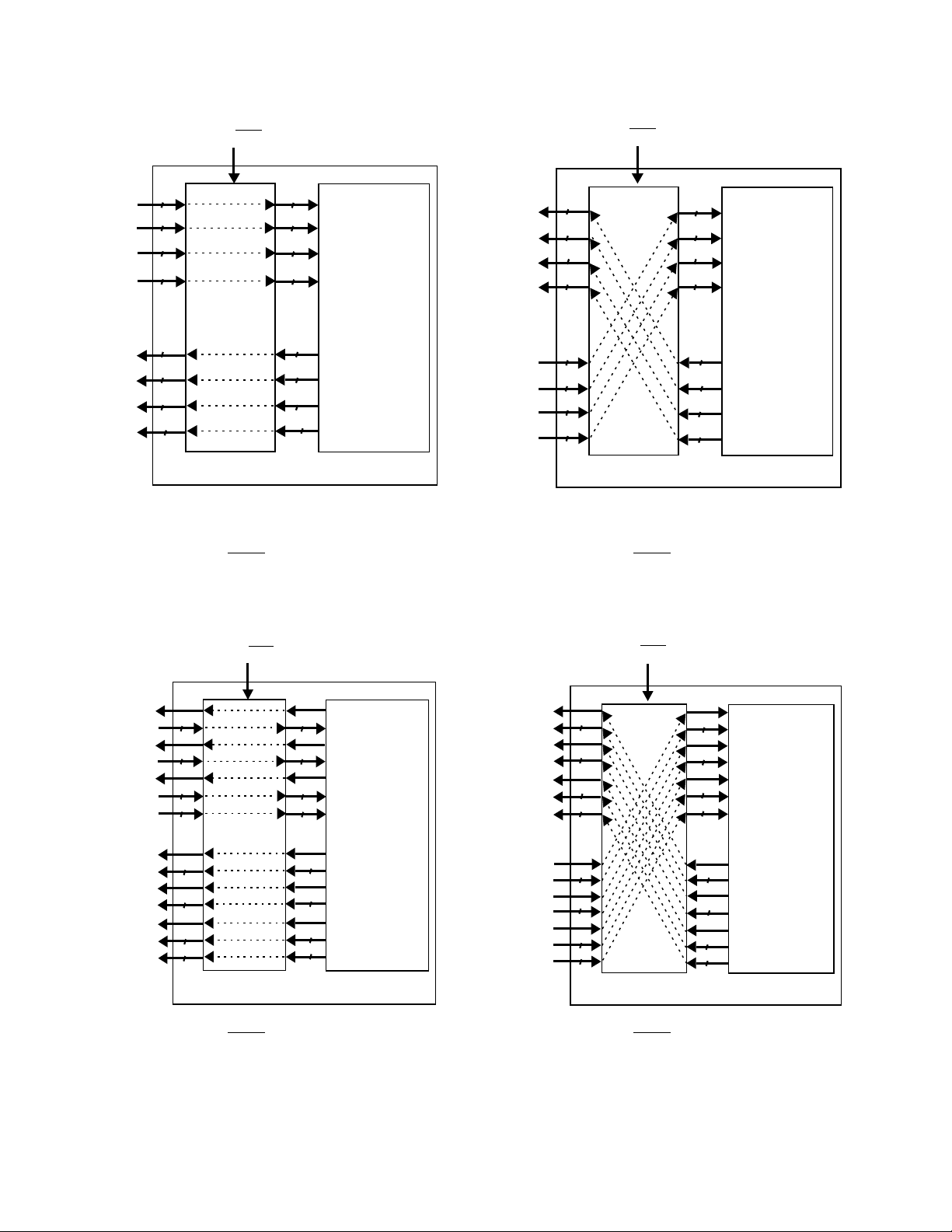
The GF9105A has 8 bi-directional data ports, labelled P1 to P8. P1 to P3 and P5 to P7 are 13-bit data ports while P4 and P8
are 11-bit data ports. The OUTPUT/INPUT
control bit and the HVF_OUT control bit (
See Host Programming Section
and
figures 4a - 4d) control how P1 to P8 are configured.
When OUTPUT/INPUT
data ports and P5
When OUTPUT/INPUT
data ports and P5
is set low and when HVF_OUT is set low, P1
12..0
, P6
12..0
, P7
12..0
, P8
are configured as output video data ports (refer to Figure 4a).
10..0
is set low and when HVF_OUT is set high, P1
12..0
, P6
12..0
, P7
12..0
, P8
are configured as output video data ports. In this mode, P112, P212, P312 are
10..0
configured as outputs for H, V, and F output data. P1
carries H data, P212 carries V data and P312 carries F data (refer to
12
12..0
11..0
, P2
, P2
12..0
11..0
, P3
, P3
12..0
11..0
, P4
, P4
are configured as input video
10..0
are configured as input video
10..0
Figure 4c).
When OUTPUT/INPUT is set high and when HVF_OUT is set low, P1
video data ports and P5
When OUTPUT/INPUT
video data ports and P5
12..0
, P6
12..0
, P7
12..0
, P8
are configured as input video data ports (refer to Figure 4b).
10..0
is set high and when HVF_OUT is set high, P1
12..0
, P6
12..0
, P7
12..0
, P8
are configured as input video data ports. In this mode, P112, P212, P3
10..0
12..0
11..0
, P2
, P2
12..0
11..0
, P3
, P3
12..0
11..0
, P4
, P4
are configured as output
10..0
are configured as output
10..0
12
are configured as outputs for HVF output data. P112 carries H data, P212 carries V data and P312 carries F data (refer to
Figure 4d).
Note: No bi-directional I/Os should be driven until after the OUTPUT/INPUT and the HVF_OUT control bits have been set
(unless DP_EN
is set high to tri-state the outputs). This will ensure that any potential conflicts between input and output data
buses are avoided.
OUTPUT/INPUT AND HVF CONTROL BIT
OUTPUT/INPUT HVF_OUT DESCRIPTION
00P1
, P2
, P6
12..0
12..0
, P3
, P7
P5
12..0
12..0
Refer to Figure 4a.
12..0
12..0
, P4
are configured as input video data ports.
10..0
, P8
are configured as output video data ports.
10..0
, P2
, P3
, P4
01P1
11..0
11..0
11..0
, P212, P312 are configured as H, V and F outputs, respectively.
P1
12
P5
, P6
12..0
, P7
12..0
12..0
are configured as input video data ports.
10..0
, P8
are configured as output video data ports.
10..0
Refer to Figure 4c.
, P2
, P3
, P4
10P1
P5
12..0
12..0
, P6
12..0
12..0
, P7
12..0
12..0
are configured as output video data ports.
10..0
, P8
are configured as input video data ports.
10..0
Refer to Figure 4b.
, P2
, P3
, P4
11P1
11..0
11..0
11..0
, P212, P312 are configured as H, V and F outputs, respectively.
P1
12
P5
, P6
12..0
, P7
12..0
12..0
are configured as output video data ports.
10..0
, P8
are configured as input video data ports.
10..0
Refer to Figure 4d.
For H, V, F output timing refer to the Timing Reference Signal Section of this data sheet.
521 - 88 - 03
8

DATA PORT ENABLE
is used for synchronously enabling and disabling the bi-directional data ports of the GF9105A. When DP_EN is set
DP_EN
high, the data ports are disabled and set to a high impedance state. When DP_EN
is set low, all data ports are enabled.
DP_EN
CONTROL PIN
DP_EN DESCRIPTION
0 Output data ports enabled.
1 Output data ports disabled (high impedance state).
INPUT CLOCK (CLK)
For standard video signals, the clock input (CLK) of the GF9105A runs at one of three rates: 13.5/18MHz, 27/36MHz or
54MHz. The 18 MHz and 36 MHz variations on main clock frequencies are used in 16 x 9 video applications where luminance
is sampled at 18 MHz. The use of a 27/36MHz clock with the GF9105A is the most common application. These clocks can be
used with any format of input or output data with the exception of single link mode. Figures 7a and 7c show multiplexed and
non-multiplexed input data with a 27/36MHz clock. When the GF9105A is used with either SMPTE RP174 compliant single link
input or output data, the input clock must run at 54 MHz (see Figure 7b).
A 13.5/18 MHz input clock speed can only be used when both the input and output data are in a non multiplexed format (see
Figure 7d). This clock rate was added to the GF9105A for use when the device is operating with non-multiplexed input and
output data, since in this case a 27.0MHz clock may not be available. To use the 13.5 MHz input clock rate, the LOWF control
bit must be set HIGH. When input clock rates of 27.0 MHz or 54.0 MHz are used, the LOWF control bit must be set LOW.
Please note, when using the GF9105A with non-multiplexed 4:2:2:4 or 4:4:4:4 input data and an input clock rate of 27/36MHz,
two rising edges of the 27/36MHz input clock are required to latch in a 13.5/18MHz input data rate (see Figure 7c).
INPUT CLOCK SUMMARY
INPUT CLOCK RATE (MHz) MODES
13.5/18 MHz Non-multiplexed Input Data
AND
Non-multiplexed Output Data (LOWF=1)
27/36 MHz All Input / Output Data Formats
EXCEPT Single Link
54 MHz SMPTE RP174 Single Link Input
OR Output Data
BASIC OPERATION OF THE GF9105A
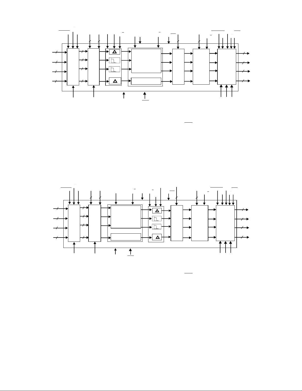
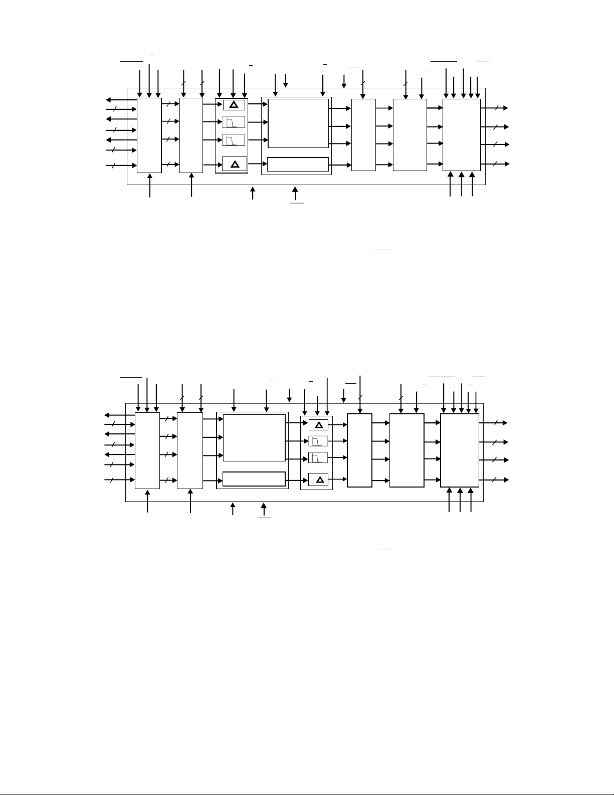
The basic operating mode for the GF9105A is selected via the INT/DEC
control bit (
effective block diagram of the GF9105A Processing Core depends on the state of INT/DEC
See Host Programming Section
. When INT/DEC is set high, the
). The
internal FIR filters are set for interpolation and are placed in front of the programmable 3X3 color space converter. Refer to
Figures 5a and 5c for a functional block diagram of the GF9105A processing core when INT/DEC
is set high. When INT/DEC
is set low, the internal FIR filters are set for decimation and are placed after the programmable 3X3 color space converter.
Refer to Figures 5b and 5d for a functional block diagram of the GF9105A with INT/DEC
set low. In these figures, static
control bits (signals loaded via the asynchronous parallel interface) are shown at the top of the diagram and control signals
with dedicated input pins are shown at the bottom of the diagram.
INT/DEC CONTROL BIT
INT/DEC DESCRIPTION
0 FIR filters set for decimation.
FIR filters placed after the 3X3 multiplier as in Figure 5b and 5d.
1 FIR filters set for interpolation.
FIR filters placed before the 3x3 multiplier as in Figure 5a and 5c.
9
521 - 88 - 03

There are seven basic blocks that make up the GF9105A. These are:
• Input De-multiplexer
• Horizontal Blanking and Input Offset Adjustment
• FIR Filters
• 3x3 Color Space Converter and KEY Scaler
• Output Offset Adjustment
• Output Clipping
• Output Multiplexer
Since the GF9105A Processing Core functionality depends on the state of INT/DEC
for the case where INT/DEC
is set high and then for the case where INT/DEC is set low.
, device operation will be described first
GF9105A OPERATION IN INTERPOLATION MODE (INT/DEC = 1)
Refer to Figures 5a and 5c for a functional block diagram of GF9105A operation with INT/DEC = 1
BIT WEIGHTING
Although the input data ports are physically 13 bits or 11 bits wide, the GF9105A Processing Core is limited to processing
10 or 8-bit unsigned input data while INT/DEC
is set high. It should be noted that while INT/DEC is set low, the GF9105A
Processing Core will accept up to 13 bit input data. Refer to later sections for a description of Processing Core functionality
while INT/DEC
is set low.
As mentioned above, the GF9105A is limited to processing 10 or 8-bit unsigned input data while INT/DEC is set high. This
input data must be properly embedded within the input data ports. The following table illustrates how to properly embed 10
or 8-bit data within the 13 bit data ports. Note that when OUTPUT/INPUT
corresponds to b
) are outputs rather than inputs. These 3 outputs are used for presenting output H, V and F output signals.
12
=0 and HVF_OUT=1, P112, P212 and P312 (which
The user should be careful to ensure that P112, P212 and P312,are not driven by upstream logic when OUTPUT/INPUT=0 and
HVF_OUT=1. Other unused inputs should be set low by the user.
OUTPUT/INPUT = 0, HVF_OUT = 0 13 BIT PHYSICAL INTERFACE
DATA PORT REFERENCE
Input Port: P1
12..0
to P3
12..0
b
12
b
11b10b9
000b
b
b
b
b
b
b
b
b
8
7
6
5
4
3
2
b
b
b
b
b
b
9
8
7
6
5
4
b
3
2
b
1
0
b
b
1
0
Embedded 10 bit signal
Input Port: P4
10..0
NA NA 0 b
b
b
b
b
b
b
b
b
9
8
7
6
5
4
3
2
b
1
0
Embedded 10 bit signal
Input Port: P1
12..0
to P3
12..0
000b
b
7
b
b
b
b
b
b
6
5
4
3
2
1
0
00
Embedded 8 bit signal
Input Port: P4
10..0
NA NA 0 b
b
b
b
b
b
b
b
7
6
5
4
3
2
1
0
00
Embedded 8 bit signal
INPUT DE-MULTIPLEXER
The MUXED_IN and SL/DL_IN control bits (
See Host Programming Section
) determine the input data format. The MUXED_IN
control bit is used to identify whether the incoming data is in a multiplexed or non-multiplexed format. The SL/DL_IN control
bit is used to identify whether the incoming data is in a single link or dual link format.
Dual Link ( S L/ DL
While MUXED_IN
Figure 7a. The input de-multiplexer separates the 4:2:2:4 or 4:4:4:4 input signals into four channels of Y/G, C
_IN = 0)
is set low, input data is assumed to be two 10 bit streams in 4:2:2:4 or 4:4:4:4 data format as shown in
/B, CR/R and
B
KEY data. These four data streams are then passed to the next processing section.
When operating with multiplexed 4:2:2:4 or 4:4:4:4 input data, the 4:2:2 data stream enters the GF9105A Processing Core
from Processing Core input port C1. While OUTPUT/INPUT
521 - 88 - 03
=0 Processing Core port C1 corresponds to device data port P1
10

OUTPUT/INPUT = 0, HVF_OUT = 1 13 BIT PHYSICAL INTERFACE
DATA PORT REFERENCE
Input Port: P1
12..0
to P3
Embedded 10 bit signal
Input Port: P4
10..0
Embedded 10 bit signal
Input Port: P1
12..0
to P3
Embedded 8 bit signal
Input Port: P4
10..0
Embedded 8 bit signal
OUTPUT/INPUT
= 1, HVF_OUT = 0 13 BIT PHYSICAL INTERFACE
DATA PORT REFERENCE
Input Port: P5
12..0
to P7
Embedded 10 bit signal
Input Port: P8
10..0
Embedded 10 bit signal
Input Port: P5
12..0
to P7
Embedded 8 bit signal
12..0
12..0
12..0
12..0
b
12
H, V, or F
b
11b10b9
00b
output
NA NA 0 b
H, V, or F
00b
output
NA NA 0 b
b
12
b
11b10b9
000b
NA NA 0 b
000b
b
b
b
b
b
b
b
b
8
7
6
5
4
3
2
b
b
b
b
b
b
9
8
7
6
5
4
b
b
b
b
9
8
7
6
b
b
7
6
b
7
6
b
8
b
9
8
b
9
8
b
7
6
b
5
4
b
b
5
4
b
b
7
6
b
b
7
6
b
b
7
6
b
b
5
4
b
5
4
b
b
3
2
b
b
3
2
b
b
5
4
b
b
5
4
b
b
5
4
b
b
3
2
b
3
2
b
b
3
2
b
b
1
0
b
b
1
0
b
b
3
2
b
b
3
2
b
b
3
2
b
b
1
0
b
1
0
b
b
1
0
b
b
1
0
00
00
b
b
1
0
b
b
1
0
b
b
1
0
00
Input Port: P8
10..0
NA NA 0 b
b
b
b
b
b
b
b
7
6
5
4
3
2
1
0
00
Embedded 8 bit signal
OUTPUT/INPUT
DATA PORT REFERENCE
Input Port: P5
= 1, HVF_OUT = 1 13 BIT PHYSICAL INTERFACE
12..0
to P7
12..0
b
12
b
11b10b9
000b
b
b
8
b
9
8
b
7
6
b
b
7
6
b
b
b
b
b
5
4
3
2
b
b
b
5
4
b
3
2
b
1
0
b
b
1
0
Embedded 10 bit signal
Input Port: P8
10..0
NA NA 0 b
b
b
b
b
b
b
b
b
9
8
7
6
5
4
3
2
b
1
0
Embedded 10 bit signal
Input Port: P5
12..0
to P7
12..0
000b
b
7
b
b
b
b
b
b
6
5
4
3
2
1
0
00
Embedded 8 bit signal
Input Port: P8
10..0
NA NA 0 b
b
b
b
b
b
b
b
7
6
5
4
3
2
1
0
00
Embedded 8 bit signal
(refer to Figures 4a and 4c). While OUTPUT/INPUT
=1 Processing Core port C1 corresponds to device data port P5 (Refer to
Figures 4b and 4d).
The KEY:2:2 or KEY:XX:XX data enters the GF9105A Processing Core from Processing Core input port C4. While OUTPUT/
=0, Processing Core port C4 corresponds to device data port P4 (Refer to Figures 4a and 4c). While OUTPUT/
INPUT
INPUT
=1, Processing Core port C4 corresponds to device data port P8 (Refer to Figures 4b and 4d).
When MUXED_IN is set high, input data is assumed to be 4:2:2:4 or 4:4:4:4 data in a non-multiplexed format as shown in
Figure 7c. Since the incoming data is already non-multiplexed, the input data is passed on to the next processing section
unmodified. In this mode of operation, input data is presented to all four Processing Core input ports. While OUTPUT/
=0, Processing Core ports C1-C4 correspond to device data ports P1-P4 (Refer to Figures 4a and 4c). While OUTPUT/
INPUT
=1 Processing Core ports C1-C4 correspond to device data ports P5-P8 (Refer to Figure 4b and 4d).
INPUT
11
521 - 88 - 03

Single Link (SL/DL
_IN = 1)
When operating with single link input data, the 4:4:4:4 data stream (SMPTE RP174 compliant) enters the GF9105A
Processing Core from Processing Core input C1.
While OUTPUT/INPUT
OUTPUT/INPUT
mode, the input clock (CLK) is operating at 54 MHz. Also, note that the MUXED_IN
= 0 Processing Core Port C1 corresponds to device data port P1 (refer to Figures 4a and 4c). While
= 1 Processing Core Port C1 corresponds to device data port P5 (refer to Figures 4b and 4d). In this
control bit must be set low (MUXED_IN
= 0).
MUXED_IN
AND SL/DL_IN CONTROL BITS
MUXED_IN SL/DL_IN DESCRIPTION
0 0 Input is in a dual link multiplexed format.
0 1 Input is in a single link multiplexed format.
1 XX Input is in a non-multiplexed format.
SYNCHRONIZATION
In order to properly synchronize the input de-multiplexer, the GF9105A requires a SYNC_CB control signal input. For
multiplexed input data, SYNC_CB should change from high to low at the start of an even numbered CB sample. After
synchronizing the device with the incoming data stream, SYNC_CB can remain low until re-synchronization is desired. Refer
to Figure 7a for timing of SYNC_CB with a dual link multiplexed input data stream. Refer to Figure 7b for timing of SYNC_CB
with a single link multiplexed input data signal. The timing shown may be referred to as “standard SYNC_CB timing”.
In order to simplify overall system design, the HSYNC output from the GS9001 EDH Coprocessor may be used as a
SYNC_CB signal when operated with a 4:2:2 or dual link 4:4:4:4 input signal. In this mode of operation, the 10 bit multiplexed
data entering the GF9105A must be fed from the output of the GS9001 and the GF9105A’s SYNC_CB input must be fed from
the GS9001’s HSYNC output (Refer to Figure 8a). To use this mode of operation the GF9105A’s GS9001 control bit (
Host Programming Section
) must be set high. When operated with a 4:2:2 or a dual link 4:4:4:4 input signal and when the
Refer to
GS9001 control bit is set high, the GS9001’s HSYNC, VSYNC, and FIELD output signals may also be used to drive the
GS9105A’s output multiplexer. Refer to the Timing Reference Signal section for information regarding this.
When dealing with single link 4:4:4:4 input or output signals “standard” SYNC_CB timing above must be used. When using
standard SYNC_CB and HVF timing, the GS9001 control must be set low. The GS9020 may be used to provide such
standard SYNC_CB timing and HVF. When operated in this manner, the 10 bit multiplexed data entering the GF9105A must
be fed from the output of the GS9020 and the GF9105A’s SYNC_CB and HVF inputs must be fed from the GS9020’s H, V, F
outputs. The same GS9020/GF9105A configuration may also be used when interfacing the GF9105A to a standard 4:2:2 or
dual link 4:4:4:4 link input signal. In this case, the GS9001 control bit must still be set low.
GS9001 CONTROL BIT
GS9001 DESCRIPTION
0 Standard SYNC_CB and H,V,F timing. Simple interface to GS9020.
1 Modified SYNC_CB and H, V, F timing. Simple interface to GS9001.
NOTE: Standard SYNC_CB and H, V, F timing must be used when receiving or generating single link 4:4:4:4 signals.
With non-multiplexed input data, SYNC_CB must change from high to low at the start of an even-numbered CB sample. It is
important to note that SYNC_CB changes from high to low on an even-numbered CB sample and not an odd-numbered
sample. After synchronizing the device with the incoming data stream, the SYNC_CB signal can remain low until resynchronization is desired. Refer to Figure 7c for timing of SYNC_CB with non-multiplexed input data. Following the input demultiplexer, data is passed to the Horizontal Blanking section of the device.
HORIZONTAL BLANKING
When H_BLANK is high, all four channels of input are forced to a user selectable set of levels. When H_BLANK is low data is
passed through the Horizontal Blanking section of the device unmodified. Refer to Figures 10a and 10b for typical timing of
H_BLANK with multiplexed input data and Figure 10c for typical timing with non-multiplexed input data. In these figures, a
521 - 88 - 03
12
 Loading...