FEATURES
• highly optimized & flexible architecture for multirate
FIR filtering applications
• implements dual 12 tap filters operating at 40 MHz or
single 23 or 24 tap filter operating at 20 MHz maximum
data rate
• stores up to 108 fully-programmable 12 tap filters with
12 bit coefficients at each tap, dynamically
addressable in each clock cycle
• 3 flexible memory loading modes
• 20 bit pipeline for cascading up to 3 devices
• 20 bit output accumulator
• filter output negate and zero controls
• supports both symmetrical and asymmetrical FIR
filters
• 40 MHz maximum computation and input/output data
rates
™
Multi
GEN
GF9101 High
Performance Multirate Digital Filter
DATA SHEET
DESCRIPTION
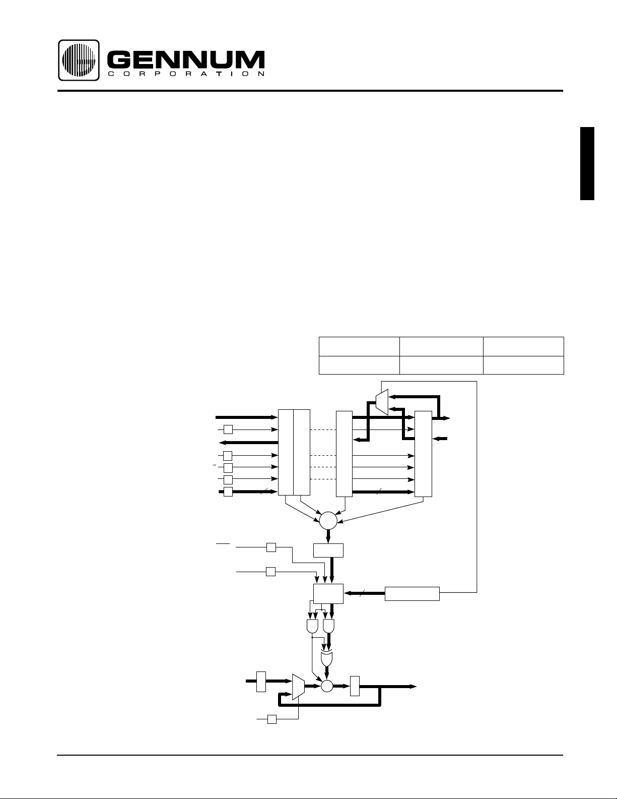
The GF9101 is a high performance multirate digital filter
which can be programmed to implement a wide range of
signal processing functions using both symmetrical and
asymmetrical filter structures. It is composed of a 12-tap
FIR filter with internal RAM to hold up to 108 individual
filters. An externally controlled address bus selects one of
the 108 filters in each clock cycle. Pipelined architecture
allows cascading of up to three devices with no additional
hardware.
Two 10-bit input shift registers are provided for multiplexed
filtering applications. The 12-bit coefficients can be
programmed in serial, high speed parallel or
microprocessor modes. In the high speed parallel mode,
any one of the 108 filters can be reprogrammed in 18 clock
cycles.
ORDERING INFORMATION
GF9101
APPLICATIONS
Video rate conversion; High performance FIR filters;
Adaptive digital filters; Video encoding; Digital modulation
+10
DATA–A–IN
ENA
R
+10
DATA–B–OUT
ENB
SEL–A/B
ENC
COEF–ADDR
R
R
R
R
ZERO
NEGATE
PIPELINE–IN
TAP
CELL
1
7
R
R
CARRY
±13.6
R
TAP
CELL
2
IN
0
1
PART NUMBER PACKAGE TEMPERATURE
GF9101 - CMQ 160 pin Metal Quad 0° to 70°C
1
TAP
CELL
11
0
TAP
CELL
7
+10
DATA–A–OUT
+10
DATA–B–IN
12
Σ
±14.11
4R
±13.6
TRUNCATED
DATA B SEL
PIPELINE–OUT
±13.6
DELAY
1,3,4,5
R
+
±13.6
±13.6
±13.6
2
DELAY SEL
±13.6
R
CONFIGURATION
REGISTER
FB–SEL
R
BLOCK DIAGRAM
Revision Date: July 1999 Document No. 520 - 64 - 7
GENNUM CORPORATION P.O. Box 489, Stn. A, Burlington, Ontario, Canada L7R 3Y3
Tel. +1 (905) 632-2996 Fax. +1 (905) 632-5946 E-mail: info@gennum.com
www.gennum.com
I/O DESCRIPTION
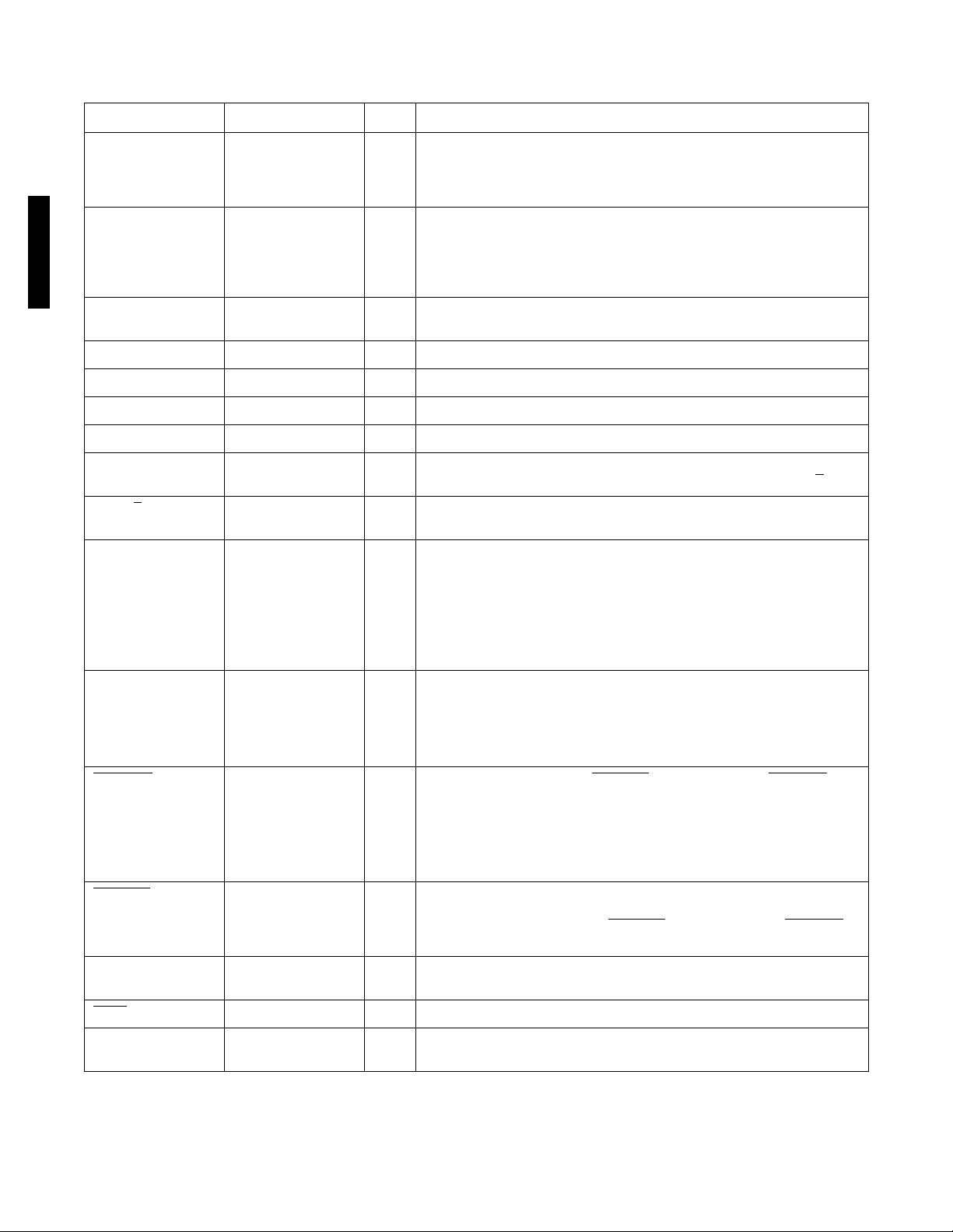
SYMBOL PIN NO. TYPE DESCRIPTION
GF9101
V
DD
1, 10, 20, 29, 40, 41,
59, 69, 80, 81, 90, 99,
+5 V power supply pins. 0.1µF capacitors between the V
are recommended.
and GND pins
CC
109, 120, 121, 129,
140, 150, 160
GND 3, 6, 8, 19, 33, 36, 39,
Device ground.
46, 49, 60, 73, 76, 79,
83, 86, 88, 100, 113,
116, 119, 122, 125,
139, 153, 155, 159
CLK_IN 138 I System clock. All inputs except for CONFIGURE, and all internal registers are
clocked on the rising edge of CLK_IN.
DATA_A_IN (9-0) 127, 128, 130-137 I Input data to registers A0 - A11. 9 bit signed or 10 bit unsigned data.
DATA_B_IN (9-0) 141-149, 151 I Input data to registers B11 - B0. 9 bit signed or 10 bit unsigned data.
ENA 23 I Shift enable for A0 - A11. Enables shifting of A registers when high.
ENB 24 I Shift enable for B0 - B11. Enables shifting of B registers when high.
ENC 25 I Enable for C0-C11. Enables C registers when high. The C registers transfer
SEL_A/B
data from either the A or B registers depending on the state of SEL_A/B
22 I Selects A or B registers. Selects registers A when high or registers B when
.
low to be transferred to the C registers.
COEF_DATA (7-0) 96-98, 101-105 I Data bus for coefficients and configuration register:
a) Parallel and microprocessor loading modes : COEF_DATA (7-0) is used to
load 8 bit data into internal RAM.
b) Serial Loading mode: COEF_DATA (7) is used to serially load the internal
RAM.
c) Configuration mode: COEF_DATA (6-0) are inputs to the CONFIGURATION
register.
COEF_ADDR (9-0) 78, 77, 75, 74, 72, 47,
45-42
I Address bus for internal RAM (address 0 —> 107):
a) Run mode: COEF_ADDR (6-0) selects one of the 108 sets of 12 coefficients
in the internal RAM.
b) Parallel and micro-processor loading modes: Selects the internal RAM
address for the 8-bit data loading COEF_DATA (7-0).
COEF_WR
17 I Enable for COEF_DATA (7-0). LOAD_EN must be enabled for COEF_WR to
work:
a) Parallel and micro-processor loading modes : Enables COEF_DATA (7-0)
registers or loading 8 bit data in internal RAM.
b) Serial Loading mode: On a high to low transition, a one bit data gets
clocked in to the internal RAM through COEF_DATA bit 7.
LOAD_EN
18 I Used during loading mode. This signal selects a particular GF9101 device
when 2 or more share the same bus for loading. The particular GF9101
device is selected when set low. LOAD_EN
must be enabled for COEF_WR.
For a single GF9101 using the serial loading, this pin can be set low.
NEGATE 126 I This signal negates the filter sum before it enters the pipelined output section
when high.
ZERO
123 I Zeros filter sum before it enters the pipelined output section when low.
FB_SEL 124 I Feedback select. Selects data in PIPELINE_IN when low or filter sum in
PIPELINE_OUT when high to the input of the output accumulator.
520 - 64 - 7
2

I/O DESCRIPTION
SYMBOL PIN NO. TYPE DESCRIPTION
CONFIGURE 21 I GF9101 reset/configure. Resets the GF9101 when high for at least one clock
PIPELINE_IN (19-0) 38,37, 35, 34, 32-30,
28-26, 15-11, 9, 7, 5,
4, 2
DATA_A_OUT (9-0) 71, 70, 68-61 O Output data from register A11.
DATA_B_OUT (9-0) 58-50, 48 O Output data from register B0.
PIPELINE_OUT (19-0)82, 84, 85, 87, 89, 91-
95, 106-108, 110-
112, 114, 115, 117,
118
S_LOAD_CMP 16 O Serial loading complete.
SCAN_IN, SCAN_EN 157, 156 Set low.
TEST 158 Set high.
POUT, SCANOUT 152, 154 No Connect.
Note: All unused inputs of the GF9101 should be connected to GND
period. Loads COEF_DATA (6-0) into the CONFIGURATION register on a high
to low transition. This bit is set low in run mode. When CONFIGURE is high,
the GF9101 is reset but the values in the internal RAM and registers in the run
mode sections are not altered. This means that the GF9101 may be
reconfigured after the internal RAM has been loaded.
I Pipeline input. Input to the output accumulator when FB_SEL is low.
O Pipeline output. Output of the accumulator or PIPELINE_IN depending on
FB_SEL.
a) Serial loading mode: When high, indicates that all the internal RAM has
been loaded.
GF9101
GF9101 OPERATION
The GF9101 has two operating modes: the load mode and
the run mode. In the load mode, the coefficients for the
filters are written to the internal RAM. In the run mode, the
GF9101 is used to filter signals.
Before the GF9101 can filter signals, two steps must be
performed:
1. CONFIGURATION - is accomplished by writing one 7 bit
word into the CONFIGURATION REGISTER. This register
holds static operating parameters that affect both the
load mode and the run mode.
2. MEMORY LOADING - is done after configuration. The
internal RAM must be loaded with at least one of the 108
filter coefficient sets before signals can be processed.
CONFIGURATION
The GF9101 is reset by holding CONFIGURE high for at
least one clock cycle. Configuration occurs upon a high to
low transition on the CONFIGURE pin. This transition
registers COEF_DATA (6-0) into the CONFIGURATION
REGISTER. Table 1 shows the meaning of each bit in the
CONFIGURATION REGISTER.
When CONFIGURE is high, the GF9101 is reset but the
values in the internal RAM and registers in the run mode
sections are not altered. This means that the GF9101 may
be reconfigured after the internal RAM has been loaded.
MEMORY LOADING
The GF9101 contains 12 tap cells with 108 12-bit memory
locations for each tap. When loading the memory, the tap
cells must be viewed as 6 memory banks with 108 24-bit
memory locations in each bank. Each memory bank is
assigned to a pair of tap cells as shown in Table 2.
During configuration, either the parallel, microprocessor, or
serial loading is selected. When in the load mode, the
memory outputs are undefined. Please refer to the GF9101
block diagram and notice that, even though the memory
outputs are undefined, several valid outputs may be in the
processing section below the multipliers and can exit the
GF9101 correctly. This would be useful for adaptive filtering
where the tap memories can be changed while the GF9101
outputs are still valid. During power up, the internal RAM of
the GF9101 is in a random state, and is not intialized to
zero.
3
520 - 64 - 7
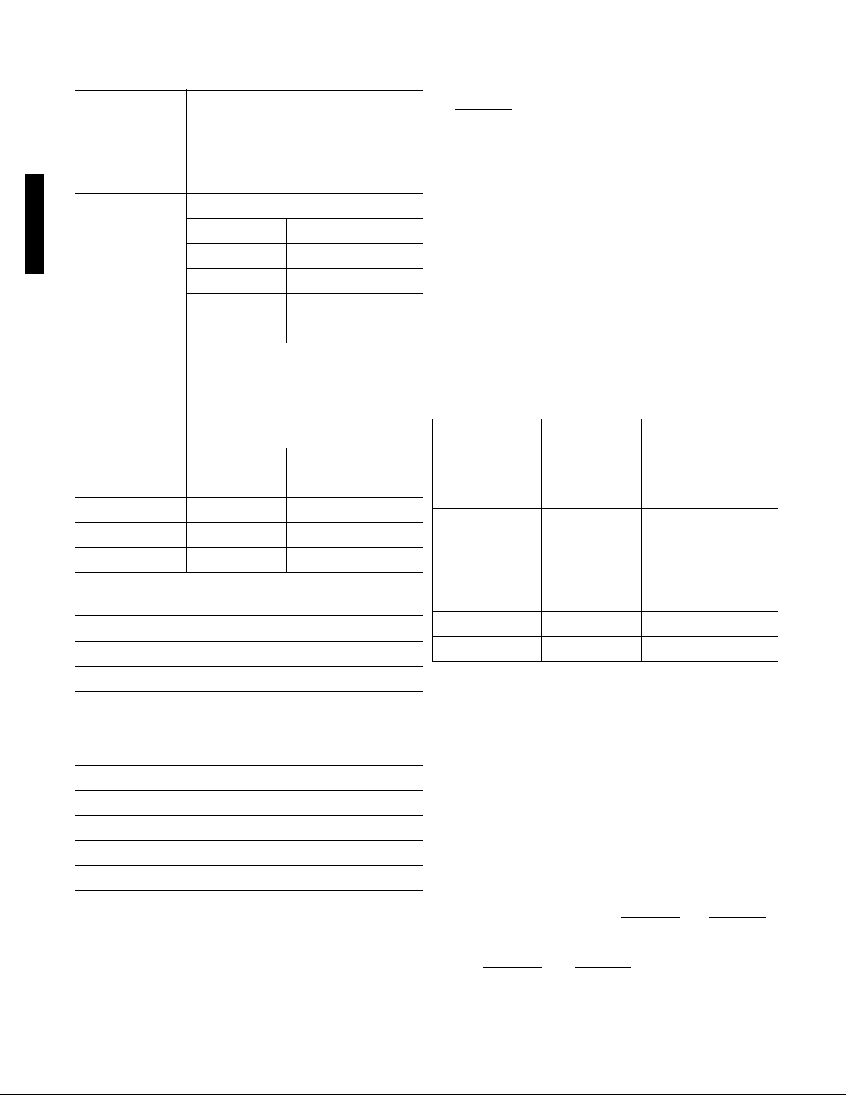
TABLE 1: Configuration Register Format
CONFIGURATION
REGISTER BIT
COEF_DATA(6-0)
0 MODE A (1 if A input signed, 0 if unsigned)
1 MODE B (1 if B input signed, 0 if unsigned)
3, 2 DELAY_SEL selects delay for pipelining:
GF9101
4 DATA_B_SEL 0 selects B12 for two 12 tap
6,5 LOAD MODE SELECT (see below)
MEANING
Bits 3, 2 Delay in CLK_IN cycles
0, 0 1
0, 1 3
1, 0 4
1, 1 5
filters or one 24 tap filter by externally
connecting DATA_A_OUT to DATA_B_IN.
DATA_B_SEL 1 selects A12 for a 23 tap
filter.
Bits 6, 5 Loading mode
0, 0 Serial
0, 1 Parallel
1, 0 Microprocessor
1, 1 Reserved
PARALLEL LOADING
If parallel loading is selected, both the COEF_WR pin and
the LOAD_EN
load mode. When COEF_WR
pin determine whether the GF9101 is in the
and LOAD_EN are both low,
the load mode is selected, the run mode is disabled, and
writes to memory can occur. Parallel loading is random
access and synchronous.
Data is written through COEF_DATA (7-0) and its destination
is determined by COEF_ADDR (9-0). Coefficient memory is
loaded by writing 8 bits at a time, first to two temporary
registers (bits 15 -0) and finally to the desired memory bank
(bits 23-0). Each memory bank word is loaded in three
clock cycles. COEF_ADDR (9-7) defines the address
location for temporary registers (TEMP_REG_A and
TEMP_REG_B) and memory banks. COEF_ADDR (6-0)
determines the filter coefficient address (0 -107) in the
internal RAM. COEF_ADDR (6-0) must be less than 108. In
Table 3, COEF_ADDR (9-7) determines the following:
TABLE 3: Temporary Loading Registers and Memory Banks
COEF_ADDR(9-7)
(binary)
111 TEMP_REG_B 8 (15-8)
110 TEMP_REG_A 8 (7-0)
101
100 MB4 24 (23-0)
011 MB3 24 (23-0)
DESTINATION NUMBER OF BITS
MB5
1
24 (23-0)
TABLE 2: Memory Locations for Internal RAM
MEMORY BANKS (BITS) TAPS (BITS)
0 (23-12) 0 (11-0)
0 (11-0) 2 (11-0)
1 (23-12) 3 (11-0)
1 (11-0) 4 (11-0)
2 (23-12) 5 (11-0
2 (11-0) 6 (11-0)
3 (23-12) 7 (11-0)
3 (11-0) 8 (11-0)
4 (23-12) 9 (11-0)
4 (11-0) 10 (11-0)
5 (23-12) 11 (11-0)
5 (11-0) 12 (11-0)
010 MB2 24 (23-0)
001 MB1 24 (23-0)
000 MB0 24 (23-0)
NOTE 1: Memory Bank No. 5
TEMP_REG_A and TEMP_REG_B temporarily hold memory
bits, (7-0) and (15-8) respectively. Three 8 bit writes are
necessary to write one 24-bit memory as follows:
1. Load COEF_DATA (7-0) into TEMP_REG_A
2. Load COEF_DATA (7-0) into TEMP_REG_B
3. Load COEF_DATA (7-0), TEMP_REG_B (7-0), and
TEMP_REG_A (7-0) into the selected memory bank, MB0MB5 (23-0).
While COEF_ADDR (9-7) selects MB0-MB5 for writing,
COEF_ADDR (6-0) selects the memory bank location that
the 24-bit word is written into. Parallel loading is
synchronous with CLK_IN. When COEF_WR
and LOAD_EN
are both low, 8-bit words will be written on the rising edge of
CLK_IN. Consecutive writes may be done indefinitely by
keeping COEF_WR
and LOAD_EN low. A parallel loading
timing diagram is shown in Figure 1.
520 - 64 - 7
4
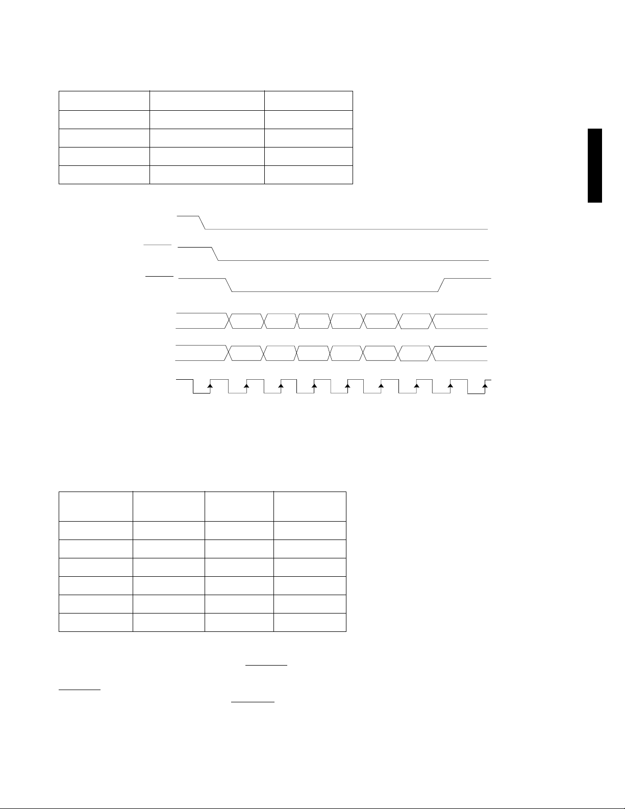
The timing diagram shown in Figure 1 loads the memories shown in Table 4:
TABLE 4: Memory Loaded into Internal RAM in Parallel Load Mode
TAP (location) 12-bit WORD IN HEX. MEMORY BANK
1 (0) FB2 MB0
2 (0) EF4 MB0
11 (107) CCC MB5
12 (107) DDD MB5
CONFIGURE
LOAD_EN
COEF_WR
COEF_DATA
(7-0)
COEF_ADDR
(9-0)
CLK_IN
XX
XX
The address generated is shown in Table 5.
F4
300
2E FB DD CD CC XX
3EB36B000 380
Fig. 1 Parallel Loading Timing Diagram
2EB
GF9101
XX
Timing for the parallel loading signals is the same as that
for other synchronous inputs.
TABLE 5: Address Generation for Parallel Loading Example
DESTINATION
COEF_ADDR
(9-7) IN BINARY
COEF_ADDR
(6-0) IN HEX
COEF_ADDR
(9-0) IN HEX
TEMP_REG_A 110 X 300
TEMP_REG_B 111 X 380
MB0 000 0 000
TEMP_REG_A 110 X 36B or 300
TEMP_REG_B 111 X 3EB or 380
MB5 101 6B 2EB
MICROPROCESSOR LOADING
If microprocessor loading is selected, the LOAD_EN
pin
alone determines the run mode or the load mode. When
LOAD_EN
is disabled, but a write will not occur until COEF_WR
is low, the load mode is selected, the run mode
is low.
Microprocessor loading is random access and
asynchronous. Like parallel loading, microprocessor
loading uses COEF_DATA (7-0) and COEF_ADDR (9-0) to
write three 8-bit words for each 24-bit memory written.
Addressing is the same as for parallel loading. In
microprocessor mode, at least one set of filter coefficients
5
520 - 64 - 7
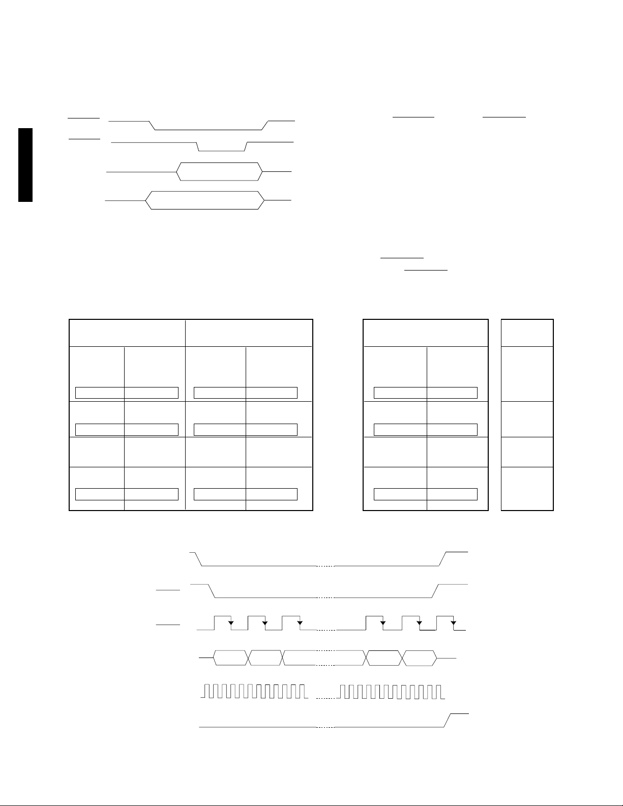
need to be loaded into the internal RAM. If location 0 is
used for filtering, MB0 > MB5 must be loaded for this
location. The example shown in Figure 2 loads the value
BB
into TEMP_REG_A.
H
LOAD_EN
COEF-WR
COEF_DATA
GF9101
(7-0)
COEF_ADDR
(9-0)
Fig. 2 Microprocessor Loading Timing Diagram
TABLE 6: Serial Mode Loading Order
300
BB
H
H
SERIAL LOADING
Serial loading is sequential and synchronous. If serial
loading is selected the GF9101 will not enter the run mode
until the entire serial load sequence is completed at which
time the S_LOAD_CMP signal will go high. A bit will be
written each time LOAD_EN
is low and COEF_WR makes a
high to low transition. Once the GF9101 is configured for
serial loading, 24 x 108 x 6 =15552 bits must be written
before the run mode is entered automatically. The 15552
bits must be entered in the order defined in Table 6. MB0 is
loaded first from RAM location 0 starting to fill the first 12
bits of tap 2. MB5 RAM location 107, tap 11 is loaded last.
When the serial load sequence is completed,
S_LOAD_CMP will go high and the run mode will be active.
Below is a serial loading timing diagram. This example
shows the serial loading start-up sequence. Notice that the
falling edge of COEF_WR
The frequency of COEF_WR
is used to register the serial data.
should be ≤1/4 CLK_IN
frequency.
Memory Bank 0 Memory Bank 1 Memory Bank 5 Ram
TAP 2 TAP 1 TAP4 TAP 3
1,2,3 .... 12 13 ........ 24 2593 ............................. 2617
0,1,2 .... 11 0 .......... 11 0 .......... 11 0 .......... 11
25 .................................. 48 2618 ............................. 2642
0 .......... 11 0 .......... 11 0 .......... 11 0 .......... 11
..........
2568 ............................. 2592 5160 ............................. 5184
0,1,2 .... 11 0 .......... 11 0 .......... 11 0 .......... 11
..........
CONFIGURE
LOAD_EN
..........
..........
TAP12 TAP 11
...............
5185 ............................. 5208
0 .......... 11 0 .......... 11
5209 ............................. 5233
...............
0 .......... 11 0 .......... 11
..........
15528 ...........................15552
...............
0 .......... 11 0 .......... 11
..........
Location
0
1
..........
107
520 - 64 - 7
COEF_WR
COEF_DATA (7)
CLK_IN
S_LOAD_CMP
BIT 1
BIT 2
BIT 3
Fig. 3 Serial Mode Timing Diagram
6
BIT 15551 BIT 15552
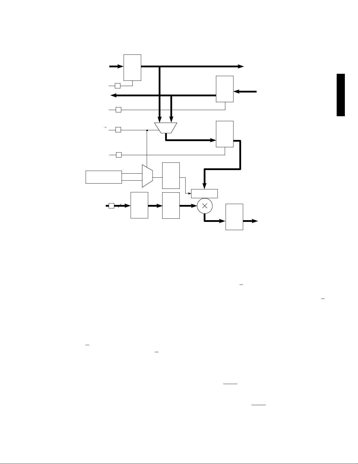
FILTER ARCHITECTURE
For the following discussion on filter architecture, refer to the GF9101 Block Diagram and Figure 4.
DATA _A_IN
ENA
TO NEXT
TAP
ENB
SEL
A/B
–
ENC
CONFIGURATION
REGISTER
COEF–ADDR
+10.0
R
108 x12
COEF
REG
+10.0
0
1
±0.11
1 0
MULT
MODE
REG
COEF
REG
SIGNED /
UNSIGNED
+10.0 / ±9.0
±0.11
+10.0
B REG
+10.0
C REG
+10.0
±10.11
A REG
R
R
R
R
MODE A
MODE B
7
MULT
REG
TO NEXT TAP
+10.0
±10.11
GF9101
DATA_B_IN
TO ADDER
Fig. 4 Tap Cell (1-12)
COEFFICIENT MULTIPLICATION AND ADDITION STAGE
Two shift registers, A and B, are used to shift input data
through the GF9101. Notice that if DATA_B_SEL was set low
during configuration, data applied at DATA_A_IN enters at
tap 1 and exits from tap 12, while data applied at
DATA_B_IN enters at tap 12 and exits from tap 1. This gives
two 12 tap filters. If DATA_B_SEL was set high during
configuration, data applied at DATA_A_IN enters at tap 1,
reverses direction at tap 12 (bypasses REG_12B) and exits
from tap 1 on DATA_B_OUT, while DATA_B_IN is disabled.
This gives a 23 tap filter. ENA and ENB control the shifting
of the input data. The C register holds the next set of 12
input values to be applied to the multipliers.
If ENC is high, SEL_A/B
register data enters the C register. SEL_A/B
, determines whether the A or B shift
, also
determines whether the MODE A or MODE B control signal
enters the MULT_MODE register. The value in the
MULT_MODE register determineswhether theinputdatato
themultiplierisrecognized as signed or unsigned. MODE A
and MODE B are separate, static control signals which
determine signed/unsigned for A or B input data
respectively. They are common to all taps. When using the
GF9101 as a 23 or 24 tap filter (combiningREG_A and
REG_B to get a single filter output), MODE A and MODE B
should be in the same state. If not, a signed/unsigned
mismatch will occur. One needs to be cautious while using
the GF9101 as two separate filters with MODE A and MODE
B not in the same state (data entering REG_A is signed/
unsigned while in REG_B it is the opposite of REG_A) . If
ENC is low and SEL_A/B
, changes state, a signed/unsigned
mismatch will occur. To avoid an error under these
circumstances, always make ENC high after a SEL_A/B
state change.
The input values in the C register are multiplied by the
coefficient values in the COEF register and the result enters
an adder tree . The coefficients that enter the COEF register
are stored in the internal RAM and are selected by the
externally controlled COEF_ADDR (6-0) bus, which is
common to all taps. At the output of the adder tree is the
untruncated sum of taps 1 through 12.
This sum is then truncated as shown in the GF9101 Block
diagram. The sum then passes through a variable delay
along with the ZERO
and NEGATE signals. The variable
delay is provided so that complementary sums from
cascaded GF9101’s may be added together in the
pipelined output stage. The ZERO
signal zeros the sum and
the NEGATE signal negates the sum.
,
7
520 - 64 - 7
 Loading...