Gennum Corporation GC590 Datasheet

FEATURES
• current mode class H output stage
• current drive power amp
• low distortion / low noise
• low amplifier current 190
µA typical
STANDARD PACKAGING
• Chip (84 x 112 mils)
DESCRIPTION
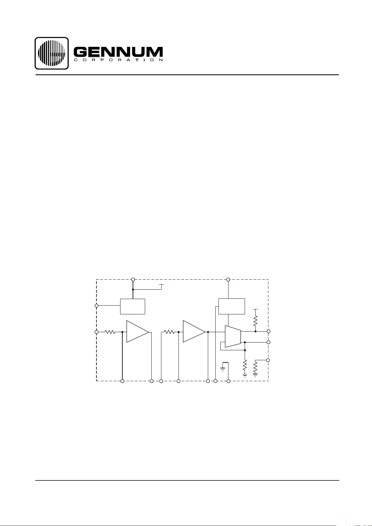
The GC590 is a linear amplifier system containing three
amplifier stages.
This product incorporates a current mode class H power
amplifier.
By adapting the bias of the output stage to the requirements
of the signal being processed, significant current savings
can be realised compared to traditional class A amplifiers.
The adaptive action does not compromise the characteristics
of a current drive output stage.
In addition to the output stage, two additional stages of
preamplification are provided to allow filtering and gain
adjustment to be easily accomplished.
Document No. 521 - 31 - 01
GC590 - DATA SHEET
Linear Class H Amplifier
GND
B
OUT
-
A
10
170
7
B
IN
24k
12k
4
6
12
11
13
5
-
GC590
A
OUT
A
IN
V
REG
REC
9
3
2
1
14
8
CONTROL
V
B
125
12k
V
REG
B
+
-
+
-
C
OUT
R
E
R
E1
V
B
C
SA
IN
B
INR
V
B
All resistors in ohms, all capacitors
in farads unless otherwise stated.
FUNCTIONAL BLOCK DIAGRAM
Revision Date: May 1998.
GENNUM CORPORATION P.O. Box 489, Stn. A, Burlington, Ontario, Canada L7R 3Y3 tel. +1 (905) 632-2996
Web Site: www.gennum.com E-mail: hipinfo@gennum.com

2
521 - 31 - 01
VB C
OUT REC
GND R
E1 AOUT
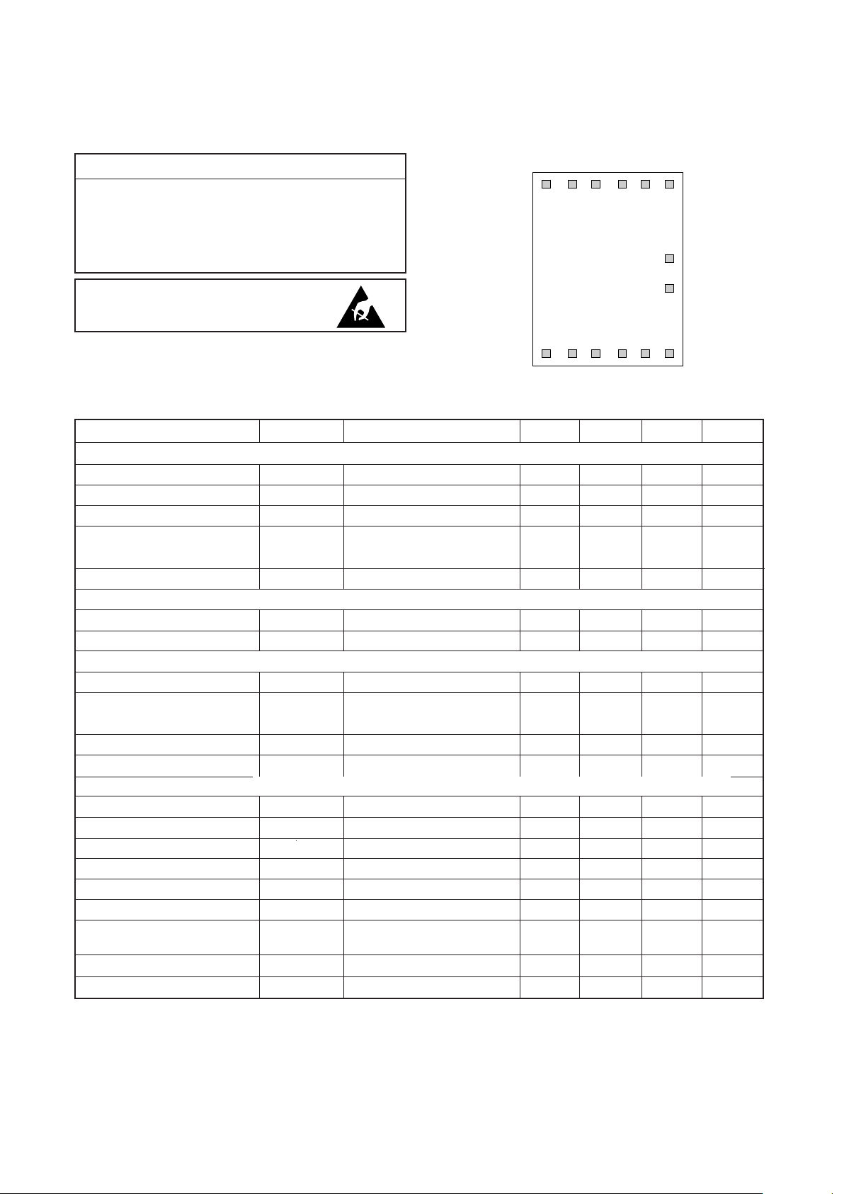
CHIP PIN CONNECTION
CAUTION
CLASS 1 ESD SENSITIVITY
ABSOLUTE MAXIMUM RATINGS
PARAMETER VALUE / UNITS
Supply Voltage 5 VDC
Power Dissipation 25 mW
Operating Temperature Range -10° C to 40° C
Storage Temperature Range -20° C to 70° C
Conditions: Frequency = 1 kHz, Temperature 25 °C, Voltage Supply = 1.3 VDC
ELECTRICAL CHARACTERISTICS
Notes: 1. Headroom = 20 Log (V
RE DC
/ V
REACRMS
) [VIN
=
-70 dBV]
A
IN
V
REG
C
SA
R
EC BIN BOUT BINR
IN
1 2 3 4 5 6
14 13 12 11 10 9
7
8
PARAMETER SYMBOL CONDITIONS MIN TYP MAX UNITS
OVERALL
Amplifier Current I
AMP
80 190 300 µA
Minimum Operating Voltage V
B
- - 1.1 V
Overall Gain A
V
51 54 57 dB
Distortion THD V
IN
= -40 dBV - 0.2 1 %
R
TRIM
= R
VC =
10 kΩ
Input Referred Noise IRN A Weighted Filter - - 2.5 µVRMS
VOLTAGE REGULATOR
Regulator Voltage V
REG
I
LOAD
= 30 µA 870 920 970 mVDC
Output Noise A Weighted - 2.9 - µVRMS
STAGE A AND STAGE B
Input Bias Current I
BIAS
-25 0 25 nA
DC Voltage Gain Stage A A
OL -A
-52 -dB
Stage B A
OL -B
-42 -dB
Current Source Capabilities I
SOURCE
15 30 - µA
Output Voltage Swing - Low V
SINK
260 315 - mV
STAGE C AND CONTROL CIRCUIT
Maximum Current Sinking I
SINK
RE grounded, V
P4
= 1.3 V 3 6 - mA
Output Impedance R
OUT
-24 -kΩ
Minimum Emitter Voltage V
RE-MIN
25 9mV
Maximum Emitter Voltage V
RE-MAX
62 66 74 mV
Minimum Transducer Current I
T-MIN
R
E, RE1
shorted 26 71 126 µA
Maximum Transducer Current I
T-MAX
R
E, RE1
shorted 750 930 1100 µA
Maximum/Minimum Transducer I
RANGE
16 20 28 dB
Current Ratio
Dynamic Headroom Headroom Note 1 14 17 22 dB
Time Constant T
C
- 100 - mS
All parameters and switches remain as shown in the Test Circuit unless otherwise stated in CONDITIONS column.
 Loading...