Gennum Corporation GC562 Datasheet

Document No. 520 - 93 - 02
GC562 - DATA SHEET
FEATURES
• direct coupled telecoil preamplifier
• natural low frequency rolloff to reduce 50/60 Hz
hum pickup
• low current consumption (typ 65 µA)
• 34 dB maximum gain
STANDARD PACKAGING
• Chip (28 x 56 mils)
Au Bump
Telecoil Preamplifier
T
IN
B
V
B
4
2
1
3
5
- A
T
OUT
GND
T
REF
FUNCTIONAL BLOCK DIAGRAM
Revision Date: September 1999
GENNUM CORPORATION P.O. Box 489, Stn. A, Burlington, Ontario, Canada L7R 3Y3 tel. +1 (905) 632-2996
Web Site: www.gennum.com E-mail: hipinfo@gennum.com
DESCRIPTION
The GC562 was designed to allow direct coupling of the
telecoil onto the preamplifier without the need of a capacitor.
The DC bias voltage at the output of the unity gain, inverting
preamplifier B, precisely matches that of the input of
preamp A. When the telecoil is placed between these two
pins, no DC current will flow through the coil as the potential
at both ends is equal. With stage B configured as unity gain,
its output appears as a virtual ground to AC signals. The lower
-3 dB corner frequency of the amplifier is set by the ratio of the
telecoil resistance to the inductance, given by the equation:
With a gain set resistor from the input to output of
preamplifier A, a signal inductively coupled into the
telecoil via the telephone will produce a signal current to flow
through the resistor, thereby producing a voltage at the output
of the amplifier.
For stability reasons it is recommended that the telecoil
amplifier not be configured for more than 34 dB gain, or with
a feedback resistor larger than 100 kΩ.
R
COIL
(2π L
COIL
)
ƒL =

2
520 - 93 - 02
PARAMETER SYMBOL CONDITIONS MIN TYP MAX UNITS
DC SPECIFICATIONS
Amplifier Current I
AMP
40 65 100 µA
Telecoil Offset Voltage T
VOFF
V
P1
- V
P3
-4 0 4 mV
Input Bias Current I
BIAS
10 100 200 nA
Stage A Source Current I
SRC_A
15 30 - µA
Stage B Source Current I
SRC_B
715 -µA
Output Voltage Swing-Low (Stage A) V
OL
50 300 - mV
AC SPECIFICATIONS
T
REF
Output Impedance Z
OUT
at < 5kHz - 200 - Ω
Input Referred Noise IRN NFB 0.2 to 10kHz at 12dB/oct - 1.5 - µVRMS
All parameters and switches remain as shown in the Test Circuit unless otherwise stated in CONDITIONS column
V
PX
- actual voltage measured on the pin at given condition (X is pin number).
CAUTION
CLASS 1 ESD SENSITIVITY
ABSOLUTE MAXIMUM RATINGS
PARAMETER VALUE / UNITS
Supply Voltage 5 VDC
Power Dissipation 25 mW
Operating Temperature Range -10° C to 40° C
Storage Temperature Range -20° C to 70° C
Conditions: Frequency = 1 kHz, Temperature = 25°C, Supply Voltage VB = 1.3 V
ELECTRICAL CHARACTERISTICS
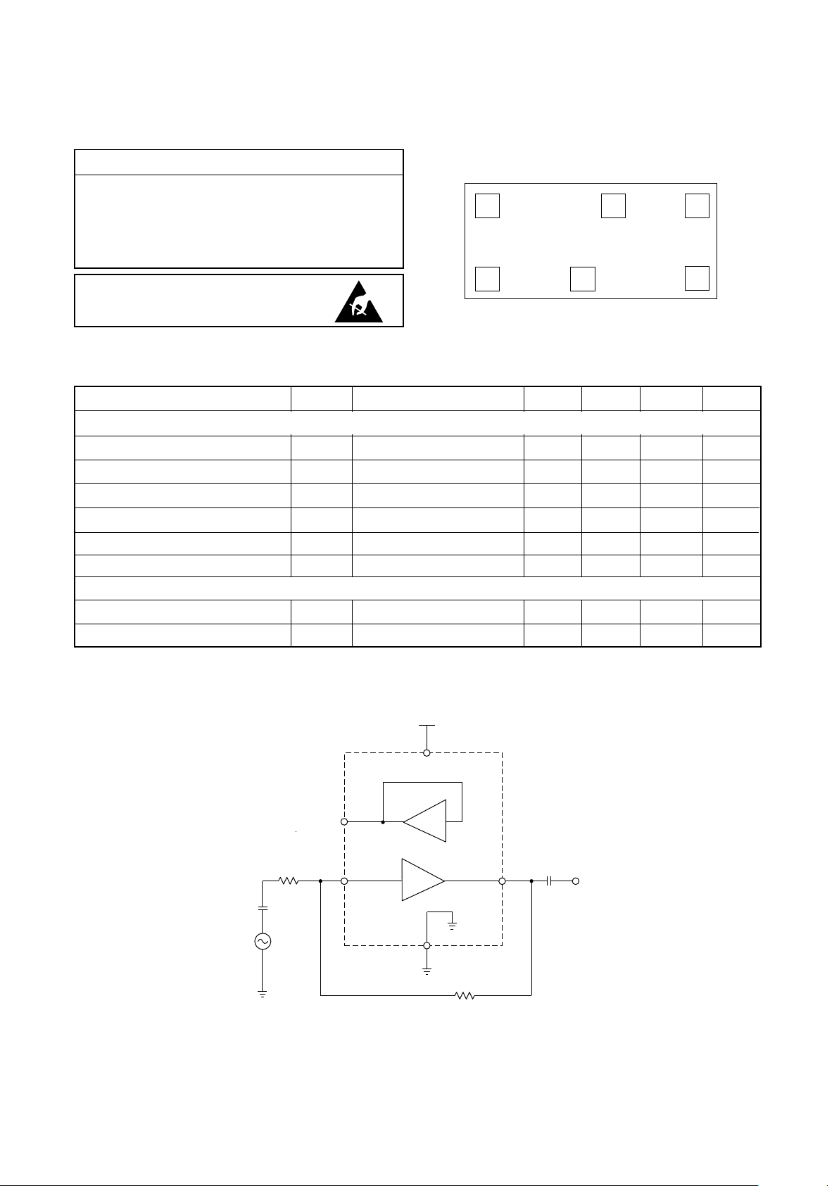
Fig. 1 Test Circuit
All resistors in ohms, all capacitors
in farads unless otherwise stated.
CHIP PIN CONNECTION
1µ0
B
V
B
=1.3V
100k
4
2
1
3
5
- A
1µ0
V
OUT
1k
T
REF
V
B
T
IN
T
REF
GND T
OUT
1 2 3
6 5 4
 Loading...