Gennum Corporation GC514 Datasheet

FEATURES
• handles high input levels cleanly
(up to 100 mVRMS)
• low THD and IMD distortion
• unique twin average detectors
• dual channel signal processing
• adjustable AGC threshold levels
• highpass filter with adjustable corner frequency
• 2:1 compression of high frequencies
STANDARD PACKAGING
• Chip (84 X 112 mils)
Au Bump
GC514 - DATA SHEET
Document No. 520 - 96 - 03
DESCRIPTION
The GC514 integrated circuit is a dynamically adaptive
loudness growth equalizer. Its gain and frequency response
are dependent on the user's environment and provide
treble increase at low levels (TILL). The unique twin
average detector circuit dramatically reduces pumping
effects and is optimized for mild-to-moderate hearing loss.
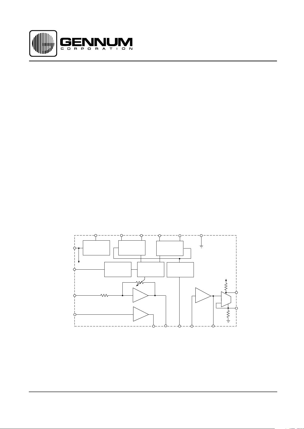
GC514 has two signal paths for dual channel processing
incorporating four amplifying stages ( A, B, C, D ) and
an AGC processing circuit.
Stage A is a highpass channel with 2:1 compression.
Stage B is a wideband buffer. The sum of the two paths
gives a high frequency boost to low level signals which
gradually compresses to a flat response at high input
levels. Stage C is used for volume control adjustment,
while stage D is a class A power amplifier with receiver
bias current adjustment.
Dynamic Equalizer Chip
4
5
C
D
+
-
+
-
24k
0.92V
8
GND
V
B
V
REG
7
15
1
14
16
2
REGULATOR
SLOW
AVERAGE
DETECTOR
FAST
AVERAGE
DETECTOR
17
R
TH
CURRENT
REFERENCE
2:1
COMPRESSION
CONTROL
12
R
E
340
C
SAD
D
OUT
11
3
9
REC
10
12k
A
B
13
6
RECTIFIER
V
B
GC514
B
IN
R
SAD
C
FAD
R
FAD
B
OUT
A
OUT
C
OUT
C
IN
A
IN
All resistors in ohms, all capacitors in farads unless otherwise stated.
Patent Pending.
FUNCTIONAL BLOCK DIAGRAM
Revision Date: May 1998
GENNUM CORPORATION P.O. Box 489, Stn. A, Burlington, Ontario, Canada L7R 3Y3 tel. +1 (905) 632-2996
Web Site: www.gennum.com E-mail: hipinfo@gennum.com

2
520 - 96 - 03
PARAMETER SYMBOL CONDITIONS MIN TYP MAX UNITS
Amplifier Current I
AMP
V
IN
= 0 VRMS 120 230 330 µA
Minimum Voltage V
B
1.1 - - V
STAGE A
Input Impedance Z
IN A
-12 -kΩ
Maximum Gain (no compression) A
MAX A
S3, S4 closed; VIN = -80 dBV 24.5 26.5 30 dB
Minimum Gain A
MIN A
VIN = -20 dBV - -11 - dB
Gain in Compression A
COMP A
S3 closed; VIN = -80 dBV 16.7 18.2 19.7 dB
High Level Distortion THD
A
VIN = -20 dBV - 0.4 2.0 %
Compression Ratio COMP VIN = -80 dBV and -60 dBV 1.74:1 1.95:1 2.11:1 Ratio
AGC
Threshold V
THR
- -94 - dBV
STAGE B
Input Bias Current I
BIAS B
02555nA
Output Source Capacity I
SOURCE B
V
P12
= 0.4 V; V
P13
= 0.5 V 15 30 - µA
Output Voltage Sink V
SINKLOW B
Note 1 200 300 500 mV
STAGE C
Input Bias Current I
BIAS C
-25 - 25 nA
Output Source Capacity I
SOURCE C
VP9 = 0.4 V; V
P10
= 0.5 V 15 30 - µA
Output Voltage Sink V
SINKLOW C
Note 2 200 300 500 mV
STAGE D
Minimum Transducer Current I
TRMIN
130 160 190 µA
Maximum Current Sink I
SINK
S1 closed 3 6 - mA
Output Impedance Z
OUT
20 24 28 kΩ
Emitter Bias Voltage V
RE
48 52 56 mV
REGULATOR
Regulator Voltage V
REG
0.89 0.92 0.97 V
Supply Rejection PSRR - 57 - dB
All parameters and switches remain as shown in the Test Circuit unless otherwise stated in CONDITIONS column
V
QX
quiescent (unbias) voltage measured on the pin, (nothing connected to the pin)
V
PX
actual voltage measured on the pin at given condition (X is pin number)
CAUTION
CLASS 1 ESD SENSITIVITY
ABSOLUTE MAXIMUM RATINGS
PARAMETER VALUE / UNITS
Supply Voltage 5 VDC
Power Dissipation 25 mW
Operating Temperature Range -10° C to 40° C
Storage Temperature Range -20° C to 70° C
Conditions: Frequency = 1 kHz, Temperature = 25°C, Supply Voltage V
B
= 1.3 V
ELECTRICAL CHARACTERISTICS
Notes: 1. V
SINKLOW B
= V
Q13
- V
P13
[I
P12
= 1 µA, I
P13
= 15 µA ]
2. V
SINKLOW C
= V
Q10
- V
P10
[I
P9
= 1 µA, I
P10
= 15 µA ]
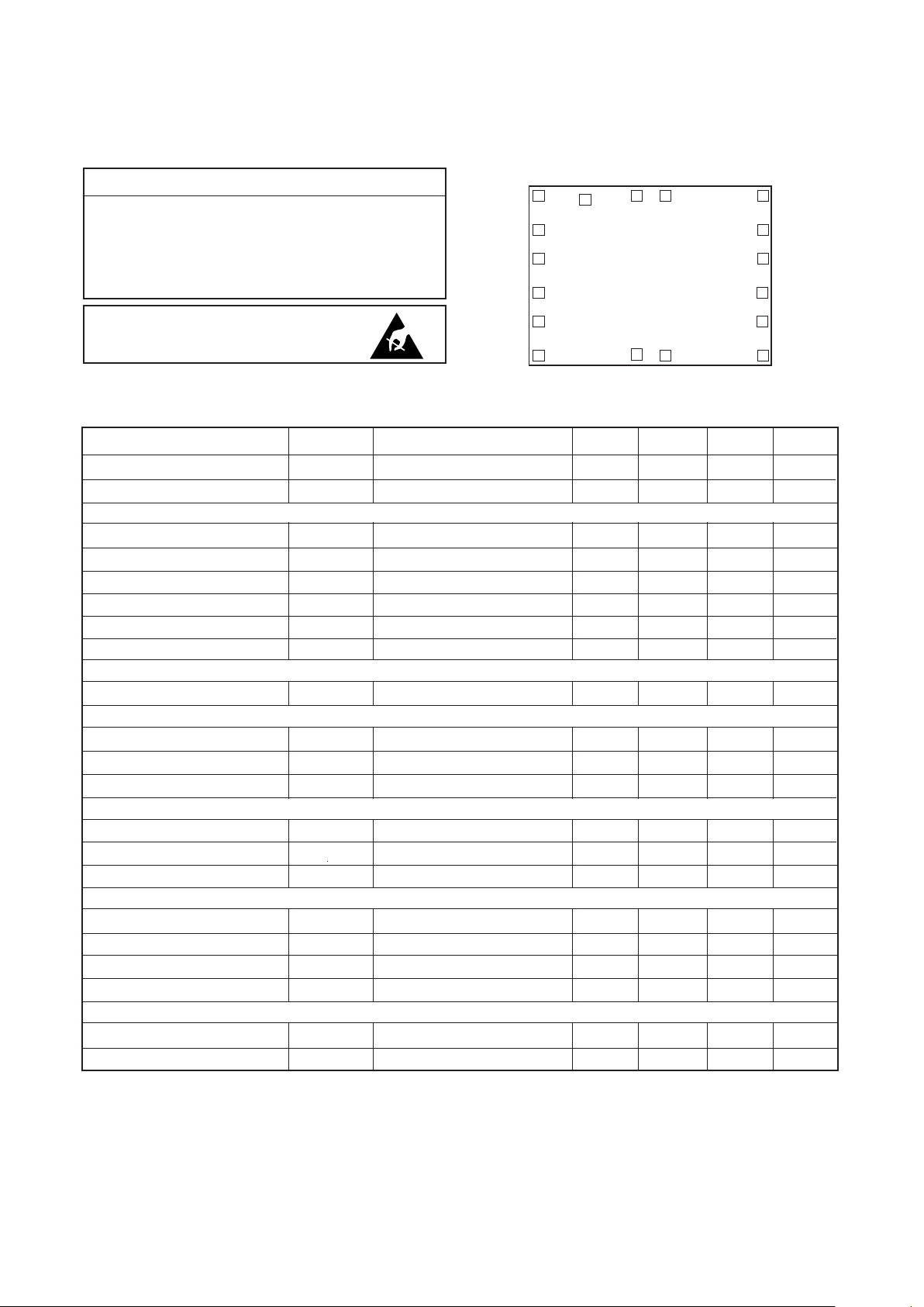
CHIP PAD CONNECTION
C
SAD
R
FAD
R
TH
C
FAD
B
OUT
B
IN
REC
C
OUT
R
SAD
GND
A
IN
R
E
D
OUT
C
IN
V
REG
V
B
5
A
OUT
6
4
3
2
7
8
9
10
11
1
12
13
14
1716
15
 Loading...