
查询GS9090供应商
GS9090 GenLINX® III 270Mb/s
Deserializer for SDI and DVB-ASI
GS9090 Data Sheet
Key Features
• SMPTE 259M-C compliant descrambling and NRZI
to NRZ decoding (with bypass)
• DVB-ASI sync word detection and 8b/10b decoding
• Integrated line-based FIFO for data
alignment/delay, clock phase interchange, DVB-ASI
data packet extraction and clock rate interchange,
and ancillary data packet extraction
• Integrated VCO and reclocker
• Automatic or manual selection between SMPTE
video and DVB-ASI data
• Single serial digital input buffer with wide input
sensitivity
• User selectable additional processing features
including:
• TRS, ANC data checksum, and EDH CRC error
detection and correction
• programmable ANC data detection
• illegal code remapping
• Internal flywheel for noise immune H, V, F
extraction
• Automatic standards detection and indication
• Enhanced Gennum Serial Peripheral Interface
(GSPI)
• JTAG test interface
• Polarity insensitive for DVB-ASI and SMPTE
signals
• +1.8V core power supply with optional +1.8V or
+3.3V I/O power supply
• Small footprint (8mm x 8mm)
• Low power operation (typically 145mW)
• Pb-free and RoHS compliant
Applications
• SMPTE 259M-C Serial Digital Interfaces
• DVB-ASI Serial Digital Interfaces
Description
The GS9090 is a 270Mb/s reclocking deserializer with
an internal FIFO. When used in conjunction with one of
Gennum’s SDI Cable Equalizers, a receive solution for
SD-SDI and DVB-ASI applications can be realized.
In addition to reclocking and deserializing the input data
stream, the GS9090 performs NRZI-to-NRZ decoding,
descrambling as per SMPTE 259M-C, and word
alignment when operating in SMPTE mode. When
operating in DVB-ASI mode, the device will word align
the data to K28.5 sync characters and 8b/10b decode
the received stream.
The integrated reclocker features a very wide Input
Jitter Tolerance, and is fully compatible with both
SMPTE and DVB-ASI input streams.
The GS9090 includes a range of data processing
functions such as error detection and correction,
automatic standards detection, and EDH support. The
device can also detect and extract SMPTE 352M
payload identifier packets and independently identify
the received video standard. This information is read
from internal registers via the host interface port.
TRS errors, EDH CRC errors, and ancillary data
checksum errors can all be detected and corrected. A
single DATA_ERROR
inverted logical 'OR'ing of all detectable errors.
Individual error status is stored in internal
‘ERROR_STATUS’ registers.
The GS9090 also incorporates a video line-based FIFO.
This FIFO may be used in four user-selectable modes
to carry out tasks such as data alignment / delay, clock
phase interchange, MPEG packet extraction and clock
rate interchange, and ancillary data packet extraction.
Parallel data outputs are provided in 10-bit multiplexed
format, with the associated parallel clock output signal
operating at 27MHz.
The GS9090 is Pb-free, and the encapsulation
compound does not contain halogenated flame
retardant (RoHS compliant).
pin is provided which is an
28201 - 1 July 2005 1 of 70
www.gennum.com
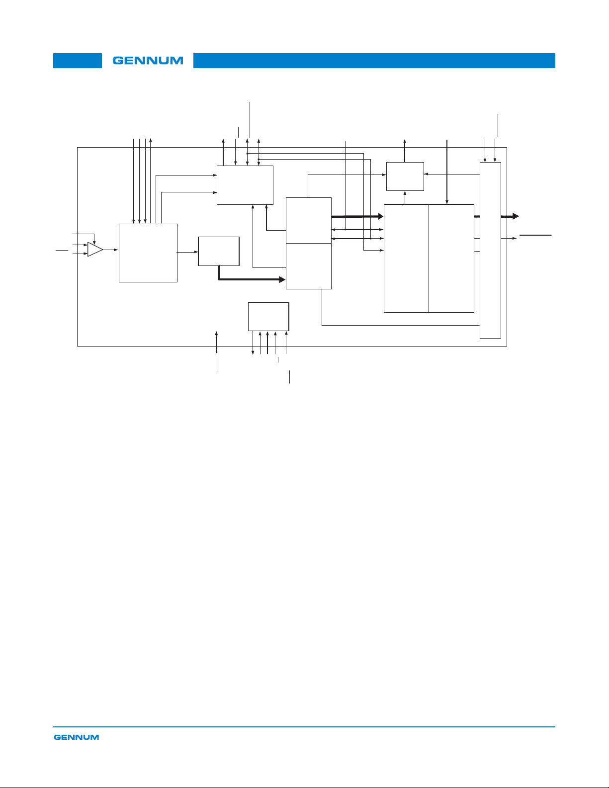
GS9090 Data Sheet
TERM
DDI_1
DDI_1
LB_CONT
LF+
LF-
Reclocker
PCLK
carrier_detect
pll_lock
S->P
RESET
AUTO/M
LOCKED
AN
LOCK detect
SMPTE_B
DVB_ASI
YPASS
SMPTE sync dete
ASI sync detect
ct
HOST Interface
/ JTAG test
SDIN_TDI
SDOUT_TDO
SCLK_TCK
CS_TMS
JTAG/HO
ST
SMPTE De-
scramble, Word
Alignment and
Flywheel
K28.5 Sync
Detect, DVB-ASI
Word Alignment
and
8b/10b Decode
FW_EN
STAT[3:0]
Programmable
I/O
TRS Check
CSUM Check
ANC Data
Detection
IOPROC_EN
TRS Correct
CSUM Correct
EDH Check &
Correct
Illegal Code Re-
map
RD_RESET
RD_CLK
FIFO
DOUT[9:0]
DATA_ERROR
GS9090 Functional Block Diagram
28201 - 1 July 2005 2 of 70

GS9090 Data Sheet
Contents
Key Features.................................................................................................................1
Applications...................................................................................................................1
Description ....................................................................................................................1
1. Pin Out .....................................................................................................................5
1.1 Pin Assignment ...............................................................................................5
1.2 Pin Descriptions ..............................................................................................6
2. Electrical Characteristics........................................................................................12
2.1 Absolute Maximum Ratings ..........................................................................12
2.2 DC Electrical Characteristics ........................................................................12
2.3 AC Electrical Characteristics.........................................................................13
2.4 Solder Reflow Profiles...................................................................................16
2.5 Host Interface Map........................................................................................17
2.5.1 Host Interface Map (R/W registers) ....................................................18
2.5.2 Host Interface Map (Read only registers) ...........................................19
3. Detailed Description ...............................................................................................20
3.1 Functional Overview .....................................................................................20
3.2 Serial Digital Input.........................................................................................21
3.3 Clock and Data Recovery .............................................................................21
3.3.1 Internal VCO and Phase Detector ......................................................21
3.4 Serial-To-Parallel Conversion .......................................................................21
3.5 Modes Of Operation......................................................................................22
3.5.1 Lock Detect.........................................................................................22
3.5.2 Auto Mode ..........................................................................................24
3.5.3 Manual Mode ......................................................................................25
3.6 SMPTE Functionality ....................................................................................25
3.6.1 SMPTE Descrambling and Word Alignment.......................................26
3.6.2 Internal Flywheel.................................................................................26
3.6.3 Switch Line Lock Handling..................................................................27
3.6.4 HVF Timing Signal Generation ...........................................................28
3.7 DVB-ASI Functionality ..................................................................................29
3.7.1 DVB-ASI 8b/10b Decoding .................................................................29
3.7.2 Status Signal Outputs .........................................................................29
3.8 Data-Through functionality ............................................................................29
3.9 Additional Processing Features ....................................................................30
3.9.1 FIFO Load Pulse.................................................................................30
3.9.2 Ancillary Data Detection and Indication ..............................................31
3.9.3 EDH Packet Detection ........................................................................33
3.9.4 EDH Flag Detection ............................................................................33
3.9.5 SMPTE 352M Payload Identifier.........................................................36
3.9.6 Automatic Video Standard and Data Format Detection......................37
28201 - 1 July 2005 3 of 70

GS9090 Data Sheet
3.9.7 Error Detection and Indication ............................................................38
3.9.8 Error Correction and Insertion ............................................................43
3.10 Internal FIFO Operation ..............................................................................46
3.10.1 Video Mode.......................................................................................46
3.10.2 DVB-ASI Mode .................................................................................48
3.10.3 Ancillary Data Extraction Mode.........................................................51
3.10.4 Bypass Mode ....................................................................................54
3.11 Parallel Data Outputs..................................................................................55
3.11.1 Parallel Data Bus ..............................................................................55
3.11.2 Parallel Output in SMPTE Mode.......................................................56
3.11.3 Parallel Output in DVB-ASI Mode.....................................................56
3.11.4 Parallel Output in Data-Through Mode .............................................56
3.12 Programmable Multi-Function Outputs .......................................................56
3.13 GS9090 Low-latency Mode.........................................................................58
3.14 GSPI Host Interface ....................................................................................59
3.14.1 Command Word Description.............................................................60
3.14.2 Data Read and Write Timing ............................................................60
3.14.3 Configuration and Status Registers ..................................................62
3.15 Reset Operation..........................................................................................63
3.16 JTAG Operation ..........................................................................................63
3.17 Device Power Up ........................................................................................64
4. References & Relevant Standards.........................................................................65
5. Application Information...........................................................................................66
5.1 Typical Application Circuit (Part A) ...............................................................66
5.2 Typical Application Circuit (Part B) ...............................................................67
6. Package & Ordering Information............................................................................68
6.1 Package Dimensions ....................................................................................68
6.2 Recommended PCB Footprint ......................................................................69
6.3 Packaging Data.............................................................................................69
6.4 Ordering Information .....................................................................................69
7. Revision History .....................................................................................................70
28201 - 1 July 2005 4 of 70
1. Pin Out
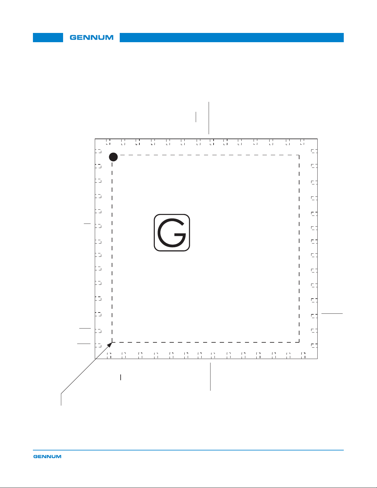
1.1 Pin Assignment
GS9090 Data Sheet
LF-
PLL_GND
PLL_VDD
BUFF_VDD
DDI
DDI
BUFF_GND
TERM
NC
VBG
NC
1
2
3
4
5
6
7
8
10
11
DVB_ASI
CORE_GND
47
LOCKED
46
45
56
LF+
VCO_GND
55
LB_CONT
54
VCO_VDD
53
FIFO_EN
52
FW_EN
51
AUTO/MAN
49
50
SMPTE_BYPASS
48
GS9090
XXXXE3
9
YYWW
PCLK
CORE_VDD
44
IO_VDD
43
42
41
40
39
38
37
36
35
34
33
IO_GND
DOUT9
DOUT8
DOUT7
DOUT6
DOUT5
DOUT4
DOUT3
DOUT2
DOUT1
GENNUM
DOUT0
32
IOPROC_EN
JTAG/HOST
RESET
Center Pad
(bottom of package)
12
13
14
15
CORE_VDD
31
RD_RESET
30
RD_CLK
29
16
CS_TMS
17
SCLK_TCK
18
CORE_GND
19
20
SDOUT_TDO
21
IO_VDD
SDIN_TDI
22
DATA_ERROR
23
25
26
STAT 1
STAT 2
28
STAT 3
24
STAT 0
IO_GND
27
IO_VDD
IO_GND
Figure 1-1: Pin Assignment
28201 - 1 July 2005 5 of 70

1.2 Pin Descriptions
Table 1-1: Pin Descriptions
GS9090 Data Sheet
Pin
Name Timing Type Description
Number
1 LF- Analog Input Loop filter component connection. Connect to pin 56 (LF+) as shown in
the Typical Application Circuit (Part B) on page 67.
2 PLL_GND Analog Input
Power
3 PLL_VDD Analog Input
Power
4 BUFF_VDD Analog Input
Power
5, 6 DDI, DDI
7 BUFF_GND Analog Input
8 TERM Analog Input Termination for serial digital input. AC couple to BUFF_GND
9, 11 NC – – No connect.
10 VBG Analog Input Bandgap filter capacitor. Connect to GND as shown in the Typical
Analog Input Serial digital differential input pair.
Power
Ground connection for phase-locked loop. Connect to GND.
Power supply connection for phase-locked loop. Connect to +1.8V DC.
Power supply connection for digital input buffers.
When operating with 1.8V input as required by the current silicon this
pin should be left unconnected.
When operating with 3.3V input (available in future silicon) this pin
should be connected to +3.3V as shown in the Typical Application
Circuit (Part B) on page 67.
Ground connection for serial digital input buffer. Connect to GND.
Application Circuit (Part B) on page 67.
12 IOPROC_EN Non
Synchronous
28201 - 1 July 2005 6 of 70
Input CONTROL SIGNAL INPUT
Signal Levels are LVCMOS / LVTTL compatible.
Used to enable or disable the I/O processing features.
When set HIGH, the following I/O processing features of the device are
enabled:
• Illegal Code Remapping
• EDH CRC Error Correction
• Ancillary Data Checksum Error Correction
• TRS Error Correction
• EDH Flag Detection
To enable a subset of these features, keep the IOPROC_EN pin HIGH
and disable the individual feature(s) in the IOPROC_DISABLE register
accessible via the host interface.
When set LOW, the device will enter low-latency mode.
NOTE: When the internal FIFO is configured for Video mode or
Ancillary Data Extraction mode, the IOPROC_EN pin must be set
HIGH (see Internal FIFO Operation on page 46).

Table 1-1: Pin Descriptions (Continued)
GS9090 Data Sheet
Pin
Name Timing Type Description
Number
13 JTAG/HOST
14 RESET
Non
Synchronous
Non
Synchronous
Input CONTROL SIGNAL INPUT
Signal levels are LVCMOS / LVTTL compatible.
Used to select JTAG Test Mode or Host Interface Mode.
When set HIGH, CS
are configured for JTAG boundary scan testing.
When set LOW, CS
are configured as GSPI pins for normal host interface operation.
Input CONTROL SIGNAL INPUT
Signal levels are LVCMOS / LVTTL compatible.
Used to reset the internal operating conditions to default setting or to
reset the JTAG test sequence.
Host Mode (JTAG/HOST
When asserted LOW, all functional blocks will be set to default
conditions and all output signals become high impedance with the
exception of the STAT pins and the DATA_ERROR
maintain the last state they were in for the duration that RESET
asserted.
JTAG Test Mode (JTAG/HOST = HIGH):
When asserted LOW, all functional blocks will be set to default and the
JTAG test sequence will be held in reset.
When set HIGH, normal operation of the JTAG test sequence resumes.
NOTE: See Device Power Up on page 64 for power on reset
requirements.
_TMS, SCLK_TCK, SDOUT_TDO, and SDIN_TDI
_TMS, SCLK_TCK, SDOUT_TDO, and SDIN_TDI
= LOW):
pin which will
is
15, 45 CORE_VDD Non
16 CS
17 SCLK_TCK Non
18, 48 CORE_GND Non
_TMS Synchronous
Synchronous
with
SCLK_TCK
Synchronous
Synchronous
Input
Power
Input CONTROL SIGNAL INPUT
Input CONTROL SIGNAL INPUT
Input
Power
Power supply for digital logic blocks. Connect to +1.8V DC.
NOTE: For power sequencing requirements, see Device Power Up on
page 64.
Signal levels are LVCMOS / LVTTL compatible.
Chip Select / Test Mode Select
Host Mode (JTAG/HOST
CS
_TMS operates as the host interface chip select, CS, and is active
LOW.
JTAG Test Mode (JTAG/HOST = HIGH):
CS
_TMS operates as the JTAG test mode select, TMS, and is active
HIGH.
Signal levels are LVCMOS / LVTTL compatible.
Serial Data Clock / Test Clock. All JTAG / Host Interface address and
data are shifted into/out of the device synchronously with this clock.
Host Mode (JTAG/HOST
SCLK_TCK operates as the host interface serial data clock, SCLK.
JTAG Test Mode (JTAG/HOST
SCLK_TCK operates as the JTAG test clock, TCK.
Ground connection for digital logic blocks. Connect to GND.
= LOW):
= LOW):
= HIGH):
28201 - 1 July 2005 7 of 70

Table 1-1: Pin Descriptions (Continued)
GS9090 Data Sheet
Pin
Name Timing Type Description
Number
19 SDOUT_TDO Synchronous
with
SCLK_TCK
20 SDIN_TDI Synchronous
21, 29, 43 IO_VDD Non
with
SCLK_TCK
Synchronous
Output CONTROL SIGNAL INPUT
Signal levels are LVCMOS / LVTTL compatible.
Serial Data Output / Test Data Output
Host Mode (JTAG/HOST
SDOUT_TDO operates as the host interface serial output, SDOUT,
used to read status and configuration information from the internal
registers of the device.
JTAG Test Mode (JTAG/HOST
SDOUT_TDO operates as the JTAG test data output, TDO.
Input CONTROL SIGNAL INPUT
Input
Power
Signal levels are LVCMOS / LVTTL compatible.
Serial Data Input / Test Data Input
Host Mode (JTAG/HOST
SDIN_TDI operates as the host interface serial input, SDIN, used to
write address and configuration information to the internal registers of
the device.
JTAG Test Mode (JTAG/HOST
SDIN_TDI operates as the JTAG test data input, TDI.
Power supply for digital I/O.
For a 3.3V tolerant I/O, connect pins to either +1.8V DC or +3.3V DC.
For a 5V tolerant I/O, connect pins to a +3.3V DC.
NOTE: For power sequencing requirements, see Device Power Up on
page 64.
= LOW):
= LOW):
= HIGH):
= HIGH):
22 DATA_ERROR
Synchronous
with PCLK
Output STATUS SIGNAL OUTPUT.
Signal levels are LVCMOS / LVTTL compatible.
The DATA_ERROR signal will be LOW when an error within the
received data stream has been detected by the device. This pin is an
inverted logical ‘OR’ing of all detectable errors listed in the internal
ERROR_STATUS register.
Once an error is detected, DATA_ERROR
start of the next video frame / field, or until the ERROR_STATUS
register is read via the host interface.
The DATA_ERROR
has been detected without error.
NOTE: It is possible to program which error conditions are monitored
by the device by setting appropriate bits in the ERROR_MASK register
HIGH. All error conditions are detected by default.
signal will be HIGH when the received data stream
will remain LOW until the
28201 - 1 July 2005 8 of 70

Table 1-1: Pin Descriptions (Continued)
GS9090 Data Sheet
Pin
Name Timing Type Description
Number
23, 25, 26, 27 STAT[0:3] Synchronous
with PCLK or
RD_CLK
24, 28, 42 IO_GND Non
Synchronous
30 RD_CLK – Input FIFO READ CLOCK
Output MULTI FUNCTION I/O PORT
Signal levels are LVCMOS / LVTTL compatible.
Programmable multi-function outputs. By programming the bits is the
IO_CONFIG register, each pin can output one of the following signals:
•H
•V
•F
• FIFO_LD
• ANC_DETECT
• EDH_DETECT
•FIFO_FULL
•FIFO_EMPTY
These pins are set to certain default values depending on the
configuration of the device and the internal FIFO mode selected. See
Programmable Multi-Function Outputs on page 56 for details.
Input
Power
Ground connection for digital I/O. Connect to GND.
Signal levels are LVCMOS / LVTTL compatible.
The application layer clocks the parallel data out of the FIFO on the
rising edge of RD_CLK.
31 RD_RESET
32 - 41 DOUT[0:9] Synchronous
44 PCLK – Output PIXEL CLOCK OUTPUT
Synchronous
with RD_CLK
with RD_CLK
or PCLK
Input FIFO READ RESET
Signal levels are LVCMOS / LVTTL compatible.
Valid input only when the device is in SMPTE mode (SMPTE_BYPASS
= HIGH and DVB-ASI = LOW), and the internal FIFO is configured for
video mode (see Video Mode on page 46).
A HIGH to LOW transition will reset the FIFO pointer to address zero of
the memory.
Output PARALLEL VIDEO DATA BUS
Signal levels are LVCMOS / LVTTL compatible.
When the internal FIFO is enabled and configured for either video
mode or DVB-ASI mode, parallel data will be clocked out of the device
on the rising edge of RD_CLK.
When the internal FIFO is in bypass mode, parallel data will be clocked
out of the device on the rising edge of PCLK.
DOUT9 is the MSB and DOUT0 is the LSB.
Signal levels are LVCMOS / LVTTL compatible.
27MHz parallel clock output.
28201 - 1 July 2005 9 of 70

Table 1-1: Pin Descriptions (Continued)
GS9090 Data Sheet
Pin
Name Timing Type Description
Number
46 LOCKED Synchronous
with PCLK
47 DVB_ASI Non
Synchronous
49 SMPTE_BYPASS
Non
Synchronous
Output STATUS SIGNAL OUTPUT
Signal levels are LVCMOS / LVTTL compatible.
The LOCKED signal will be HIGH whenever the device has correctly
received and locked to SMPTE compliant data in SMPTE mode or
DVB-ASI compliant data in DVB-ASI mode, or when the reclocker has
achieved lock in Data-Through mode.
It will be LOW otherwise. When the signal is LOW, all digital output
signals will be forced to logic LOW levels.
Input /
Output
Input /
Output
CONTROL SIGNAL INPUT / STATUS SIGNAL OUTPUT
Signal levels are LVCMOS / LVTTL compatible.
This pin is an input set by the application layer in Manual mode, and an
output set by the device in Auto mode.
Auto Mode (AUTO/MAN
The DVB_ASI signal will be HIGH only when the device has locked to a
DVB-ASI compliant data stream. It will be LOW otherwise.
Manual Mode (AUTO/MAN
When the application layer sets this pin HIGH, the device will be
configured to operate in DVB-ASI mode. The SMPTE_BYPASS
be ignored.
When set LOW, the device will not support the decoding or word
alignment of received DVB-ASI data.
CONTROL SIGNAL INPUT / STATUS SIGNAL OUTPUT
Signal levels are LVCMOS / LVTTL compatible.
This pin is an input set by the application layer in Manual mode, and an
output set by the device in Auto mode.
Auto Mode (AUTO/MAN
The SMPTE_BYPASS
locked to a SMPTE compliant data stream. It will be LOW otherwise.
When the signal is LOW, no I/O processing features are available.
Manual Mode (AUTO/MAN
When the application layer sets this pin HIGH in conjunction with
DVB_ASI = LOW, the device will be configured to operate in SMPTE
mode. All I/O processing features may be enabled in this mode.
When the SMPTE_BYPASS
the descrambling, decoding, or word alignment of received SMPTE
data. No I/O processing features will be available.
= HIGH):
= HIGH):
signal will be HIGH only when the device has
= LOW):
pin will
= LOW):
pin is set LOW, the device will not support
50 AUTO/MAN
Non
Synchronous
28201 - 1 July 2005 10 of 70
Input CONTROL SIGNAL INPUT
Signal levels are LVCMOS / LVTTL compatible.
When set HIGH, the GS9090 will operate in Auto mode. The DVB_ASI
and SMPTE_BYPASS
device. In this mode, the GS9090 will automatically detect, reclock,
deserialize, and process SMPTE or DVB-ASI compliant input data.
When set LOW, the GS9090 will operate in Manual mode. The
DVB_ASI and SMPTE_BYPASS
this mode, the application layer must set these two external pins for the
correct reception of either SMPTE or DVB-ASI data. Manual mode also
supports the reclocking and deserializing of data not conforming to
SMPTE or DVB-ASI streams.
pins become output status signals set by the
pins become input control signals. In

Table 1-1: Pin Descriptions (Continued)
GS9090 Data Sheet
Pin
Name Timing Type Description
Number
51 FW_EN Non
Synchronous
52 FIFO_EN Non
Synchronous
53 VCO_VDD Analog Input
54 LB_CONT Analog Input CONTROL SIGNAL INPUT
Input CONTOL SIGNAL INPUT
Signal levels are LVCMOS / LVTTL compatible.
Used to enable or disable the noise immune flywheel of the device.
When set HIGH, the internal flywheel is enabled. This flywheel is used
in the extraction of timing signals, the generation of TRS signals, the
automatic detection of video standards, and in manual switch line lock
handling.
When set LOW, the internal flywheel is disabled. Timing based TRS
errors will not be detected.
Input CONTOL SIGNAL INPUT
Power
Signal levels are LVCMOS / LVTTL compatible.
Used to enable / disable the internal FIFO.
When FIFO_EN is HIGH, the internal FIFO will be enabled. Data will be
clocked out of the device on the rising edge of the RD_CLK input pin if
the FIFO is in video mode or DVB-ASI mode.
When FIFO_EN is LOW, the internal FIFO is bypassed and parallel
data is clocked out on the rising edge of the PCLK output.
Power supply connection for Voltage-Controlled-Oscillator. Connect to
+1.8V DC.
Control voltage to fine-tune the loop bandwidth of the PLL.
55 VCO_GND Analog Input
Power
56 LF+ Analog Input Loop filter component connection. Connect to pin 1 (LF-) as shown in
– Center Pad – Power Connect to GND following the Recommended PCB Footprint on
Ground connection for Voltage-Controlled-Oscillator. Connect to GND.
the Typical Application Circuit (Part B) on page 67.
page 69
28201 - 1 July 2005 11 of 70

2. Electrical Characteristics
2.1 Absolute Maximum Ratings
Table 2-1: Absolute Maximum Ratings
Parameter Value/Units
Supply Voltage Core -0.3V to +2.1V
Supply Voltage I/O -0.3V to +3.47V
Input Voltage Range (any input) -2.0V to + 5.25V
GS9090 Data Sheet
Ambient Operating Temperature -20°C <
Storage Temperature -40°C <
ESD protection on all pins (see note 2) 1kV
NOTES:
1. See reflow solder profile
2. HBM, per JESDA - 114B
TA < 85°C
T
< 125°C
STG
2.2 DC Electrical Characteristics
Table 2-2: DC Electrical Characteristics
VDD = 1.8V, TA = 0°C to 70°C, unless otherwise specified.
Parameter Symbol Condition Min Typ Max Units Notes
System
Operating Temperature Range T
Core power supply voltage CORE_VDD – 1.71 1.8 1.89 V –
Digital I/O Buffer Power Supply
Voltage
A
IO_VDD 1.8V Operation 1.71 1.8 1.89 V –
IO_VDD 3.3V Operation 3.13 3.3 3.47 V –
– 0 25 70 °C 1
PLL Power Supply Voltage PLL_VDD – 1.71 1.8 1.89 V –
VCO Power Supply Voltage VCO_VDD – 1.71 1.8 1.89 V –
Typical System Power P
Max. System Power P
28201 - 1 July 2005 12 of 70
D
D
CORE_VDD = 1.8V
IO_VDD = 1.8V
o
T = 25
C
CORE_VDD = 1.89V
IO_VDD = 3.47V
o
T = 70
C
– 145 – mW –
– – 200 mW –

GS9090 Data Sheet
Table 2-2: DC Electrical Characteristics (Continued)
VDD = 1.8V, TA = 0°C to 70°C, unless otherwise specified.
Parameter Symbol Condition Min Typ Max Units Notes
Digital I/O
Input Voltage, Logic LOW V
Input Voltage, Logic HIGH V
Output Voltage, Logic LOW V
Output Voltage, Logic HIGH V
IL
IH
OL
OH
1.8V Operation or
3.3V Operation
1.8V Operation or
3.3V Operation
IOL = 8mA @ 3.3V,
4mA @ 1.8V
IOL = -8mA @ 3.3V,
-4mA @ 1.8V
– – 0.35 x
0.65 x
IO_VDD
––0.4V–
IO_VDD -
0.4
––V–
––V–
IO_VDD
V–
Serial Digital Input
Input Termination Resistance R
NOTES:
1. All DC and AC electrical parameters within specification.
IN
– 37.55062.5 Ω –
2.3 AC Electrical Characteristics
Table 2-3: AC Electrical Characteristics
VDD = 1.8V, TA = 0°C to 70°C, unless otherwise specified.
Parameter Symbol Condition Min Typ Max Units Notes
System
Asynchronous Lock Time (LOCKED
signal set HIGH)
Asynchronous Lock Time (LOCKED
signal set HIGH)
Asynchronous Lock Time (LOCKED
signal set HIGH)
t
LOCK
t
LOCK
t
LOCK
28201 - 1 July 2005 13 of 70
Input jitter of 0.2UI,
No data to SMPTE,
SMPTE_BYPASS
DVB_ASI = LOW,
at 25°C
Input jitter of 0.2UI,
No data to DVB-ASI,
SMPTE_BYPASS
DVB_ASI = HIGH,
at 25°C
Input jitter of 0.2UI,
No data to non-SMPTE,
SMPTE_BYPASS
DVB_ASI = LOW,
at 25°C
= HIGH
= HIGH
= LOW
––235us1
––185us1
––165us1

GS9090 Data Sheet
Table 2-3: AC Electrical Characteristics (Continued)
VDD = 1.8V, TA = 0°C to 70°C, unless otherwise specified.
Parameter Symbol Condition Min Typ Max Units Notes
Serial Digital Input
Serial Input Data Rate DR
SDI
– – 270 – Mb/s –
Serial Input Jitter Tolerance IJT – – 0.4 – UI 2
Serial Digital Input Signal Swing ΔV
DDI
Differential with
400 800 1700 mV
p-p
internal 100Ω input
termination
Parallel Output
Parallel Output Clock Frequency f
PCLK
Parallel Output Clock Duty Cycle DC
Variation of Parallel Output Clock
– Device Unlocked
(from 27MHz)
Output Data Hold Time t
Output Delay Time t
OH
OD
PCLK
––27–MHz–
–40–60%–
-7.5 – +7.5 % 4
= -20°C to +85°C
T
A
IO_VDD = 1.8V
With 15pF load 3.0 – – ns 5
With 15pF load – – 10.0 ns 5
GSPI
GSPI Input Clock Frequency f
GSPI
GSPI Clock Duty Cycle DC
GSPI Setup Time t
GS
GSPI
– – – 54.0 MHz –
–40–60%–
–1.5––ns–
3
GSPI Hold Time t
GH
–––1.5ns–
NOTES:
1. No signal to signal present, or a switch from another data rate to 270Mb/s.
2. Power supply noise 50mV
at 15kHz, 100kHz, 1MHz sinusoidal modulation.
pp
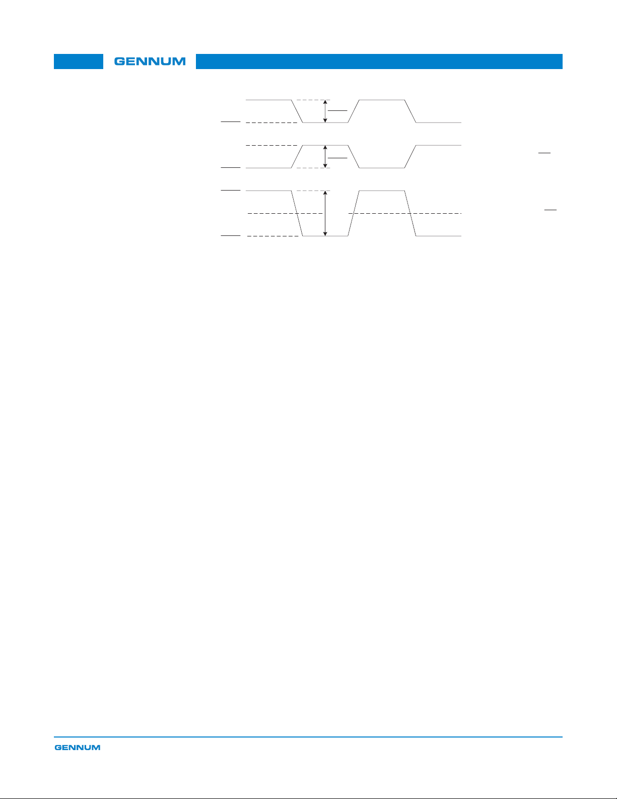
3. See Figure 2-1.
4. When the serial input to the GS9090 is removed, the PCLK output signal will continue to operate at 27MHz and the internal VCO will
remain at this frequency within +/- 7.5% over the range -20
o
C to +85oC.
5. Timing includes the following outputs: DOUT[9:0], STAT[3:0]. When the FIFO is enabled, the outputs are measured with respect to
RD_CLK.
28201 - 1 July 2005 14 of 70
GS9090 Data Sheet
DD
V
_
Δ
DDI
V
DD
V
2
V
DDI
Δ
2
Single-Ended Swing (DDI)
VDD
Δ
Δ
VDDI
2
VDDI
_
Δ
VDDI
V
DD
2
Δ
V
DDI
+
2
0
_
DDI
V
Δ
2
Figure 2-1: Serial Digital Input Signal Swing
Single-Ended Swing (DDI)
Differential Swing (DDI-DDI)
28201 - 1 July 2005 15 of 70
2.4 Solder Reflow Profiles
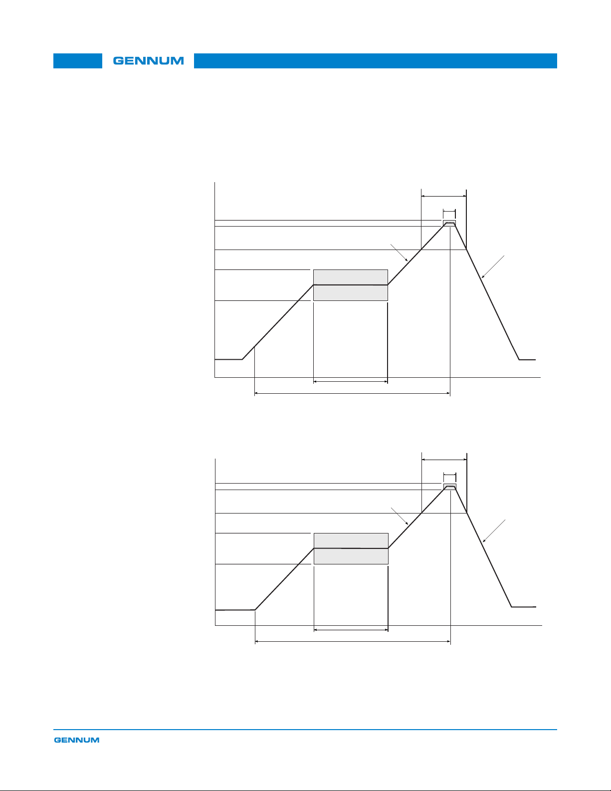
The device is manufactured with Matte-Sn terminations and is compatible with both
standard eutectic and Pb-free solder reflow profiles. MSL qualification was
performed using the maximum Pb-free reflow profile shown in Figure 2-2. The
recommended standard eutectic reflow profile is shown in Figure 2-3.
Temperature
260˚C
250˚C
217˚C
200˚C
150˚C
GS9090 Data Sheet
60-150 sec.
20-40 sec.
3˚C/sec max
6˚C/sec max
25˚C
60-180 sec. max
8 min. max
Figure 2-2: Maximum Pb-free Solder Reflow Profile (Preferred)
Temperature
230˚C
220˚C
183˚C
150˚C
100˚C
25˚C
3˚C/sec max
120 sec. max
6 min. max
60-150 sec.
10-20 sec.
Time
6˚C/sec max
Time
Figure 2-3: Standard Eutectic Solder Reflow Profile (Pb-free package)
28201 - 1 July 2005 16 of 70
DATA_
FORMAT
EAV_ERR_MA
SK
b0
STAT0_
CONFIG
b0
TRS_IN
GS9090 Data Sheet
SAV_ERR_MA
CCS_ERR_M
LOCK_
AP_CRC_
FF_CRC_
SK
ASK
ERR_
ERR_
ERR_
ERR_
ANC_
CSUM_
DATA_
FORMAT
b1
STAT0_
CONFIG
b1
DATA_
FORMAT
b2
STAT0_
CONFIG
b2
DATA_
FORMAT
MASK
MASK
MASK
MASK
b3
STAT1_
CONFIG
b0
LOCK
STAT1_
CONFIG
b1
STAT1_
CONFIG
b2
Not Used No t Used STD _
STAT2_
CONFIG
b0
VERSION_35
2M
STAT2_
CONFIG
b1
DETECT
STAT2_
CONFIG
b2
STAT3_
CONFIG
b0
INS
EDH_CRC_IN
S
CCS_ERR SAV_ERR EAV_ERR
MAP
LOCK_
ERR
AP_CRC_
ERR
Not Used No t Used ILLE GAL_RE
FF_CRC_
ERR
ERR
H_
CONFIG
FIFO_
MODE
b0
FIFO_
MODE
b1
T
).
17 of 70
AP_CRC_V FF_CRC_V EDH_
STAT3_
CONFIG
b1
Section 3.10.3
FLAG_
UPDATE
STAT3_
CONFIG
b2
DATA_
SWITCH
28201 - 1 July 2005
Not Used Not Used Not Usedb12b11b10b9b8b7b6b5b4b3b2b1b0
27h
26h
Not Used Not Used Not Usedb12b11b10b9b8b7b6b5b4b3b2b1b0
Not Used Not Used Not Usedb12b11b10b9b8b7b6b5b4b3b2b1b0
Not Used Not Used Not Usedb12b11b10b9b8b7b6b5b4b3b2b1b0
Not Used Not Used Not Usedb12b11b10b9b8b7b6b5b4b3b2b1b0
Not Used Not Used Not Usedb12b11b10b9b8b7b6b5b4b3b2b1b0
Not Used Not Used Not Usedb12b11b10b9b8b7b6b5b4b3b2b1b0
Not Used Not Used Not Usedb12b11b10b9b8b7b6b5b4b3b2b1b0
Not Used Not Used Not Usedb12b11b10b9b8b7b6b5b4b3b2b1b0
Not Used Not Used Not Used Not Used Not Usedb10b9b8b7b6b5b4b3b2b1b0
Not Used Not Used Not Used Not Used Not Usedb10b9b8b7b6b5b4b3b2b1b0
Not Used Not Used Not Used Not Used Not Usedb10b9b8b7b6b5b4b3b2b1b0
Not Used Not Used Not Used Not Used Not Usedb10b9b8b7b6b5b4b3b2b1b0
Not Used Not Used Not Used Not Used Not Usedb10b9b8b7b6b5b4b3b2b1b0
Not Used Not Used Not Used Not Used Not Usedb10b9b8b7b6b5b4b3b2b1b0
Not Used Not Used Not Used Not Used Not Usedb10b9b8b7b6b5b4b3b2b1b0
Not Used Not Used Not Used Not Used Not Usedb10b9b8b7b6b5b4b3b2b1b0
Not Used Not Used Not Used Not Used Not Usedb10b9b8b7b6b5b4b3b2b1b0
Not Used Not Used Not Usedb12b11b10b9b8b7b6b5b4b3b2b1b0
Not Used Not Used Not Usedb12b11b10b9b8b7b6b5b4b3b2b1b0
Not Used Not Used Not Used Not Used Not Usedb10b9b8b7b6b5b4b3b2b1b0
Not Used Not Used Not Used Not Used Not Usedb10b9b8b7b6b5b4b3b2b1b0
Not Used Not Used Not Used Not Used Not Usedb10b9b8b7b6b5b4b3b2b1b0
Not Used Not Used Not Used Not Used Not Used Not Used b9 b8 b7 b6 b5 b4 b3 b2 b1 b0
Not Used Not Used Not Used Not Used Not Used Not Used b9 b8 b7 b6 b5 b4 b3 b2 b1 b0
Not Used Not Used Not Used ANC_
Not Used Not Used Not Used Not Used EDH_
Not Used ANC-UES ANC-IDA ANC-IDH ANC-EDA ANC-EDH FF-UES FF-IDA FF-IDH FF-EDA FF-EDH AP-UES AP-IDA AP-IDH AP-EDA AP-EDH
Not Used ANC-UES_IN ANC-IDA_IN ANC-IDH_IN ANC-EDA_IN ANC-EDH_IN FF-UES_IN FF-IDA_IN FF-IDH_IN FF-EDA_IN FF-EDH_IN AP-UES_IN AP-IDA_IN AP-IDH_IN AP-EDA_IN AP-EDH_IN
Not Used Not Used Not Used Not Used Not Used Not Used Not Used Not Used Not Used VD_STD_
Not Used Not Used Not Used Not Used Not Used Not Used ANC_PKT_EX
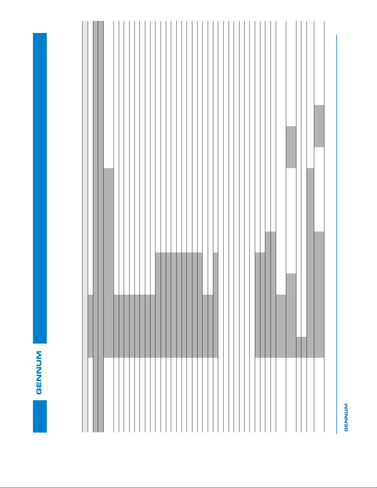
2.5 Host Interface Map
Register Name Address 15 14 13 12 11 10 9 8 7 6 5 4 3 2 1 0
Table 2-4: Host Interface Map
FIFO_LD_POSITION [12:0] 28h
FF_PIXEL_END_F1[12:0] 24h
FF_PIXEL_START_F1[12:0] 23 h
FF_PIXEL_END_F0[12:0] 22h
FF_PIXEL_START_F0[12:0] 21 h
AP_PIXEL_END_F1[12:0] 20h
ERROR_MASK_REGISTER 25h Not Used Not Used Not Used Not Used Not U sed Not Us ed Not Us ed Not Us ed Not Used VD_STD_
AP_PIXEL_START_F1[12:0] 1Fh
FF_LINE_START_F1[10:0] 1Bh
FF_LINE_END_F0[10:0] 1Ah
FF_LINE_START_F0[10:0] 19h
AP_LINE_END_F1[10:0] 18h
AP_LINE_START_F1[10:0] 17h
AP_LINE_END_F0[10:0] 16h
AP_LINE_START_F0[10:0] 15h
RASTER_STRUCTURE4[10:0] 14h
RASTER_STRUCTURE3[12:0] 13h
VIDEO_FORMAT_OUT_B(4,3) 10h VFO4-b7 VFO4-b6 VFO4-b5 VFO4-b4 VFO4-b3 VFO4-b2 VFO4-b1 VFO4-b0 VFO3-b7 VFO3-b6 VFO3-b5 VFO3-b4 VFO3-b3 VFO3-b2 VFO3-b1 VFO3-b0
VIDEO_FORMAT_OUT_A(2,1) 0Fh VFO2-b7 VFO2-b6 VFO2-b5 VFO2-b4 VFO2-b3 VFO2-b2 VFO2-b1 VFO2-b0 VFO1-b7 VFO1-b6 VFO1-b5 VFO1-b4 VFO1-b3 VFO1-b2 VFO1-b1 VFO1-b0
ANC_TYPE(5)[15:0] 0Ehb15b14b13b12b11b10b9b8b7b6b5b4b3b2b1b0
ANC_TYPE(4)[15:0] 0Dhb15b14b13b12b11b10b9b8b7b6b5b4b3b2b1b0
ANC_TYPE(3)[15:0] 0Chb15b14b13b12b11b10b9b8b7b6b5b4b3b2b1b0
ANC_TYPE(2)[15:0] 0Bhb15b14b13b12b11b10b9b8b7b6b5b4b3b2b1b0
AP_PIXEL_END_F0[12:0] 1Eh
AP_PIXEL_START_F0[12:0] 1Dh
FF_LINE_END_F1[10:0] 1Ch
RASTER_STRUCTURE2[12:0] 12h
RASTER_STRUCTURE1[10:0] 11h
ANC_TYPE(1)[15:0] 0Ahb15b14b13b12b11b10b9b8b7b6b5b4b3b2b1b0
FIFO_EMPTY_OFFSET 06h
ANC_LINE_B[10:0] 09h
IO_CONFIG 05h
ANC_LINE_A[10:0] 08h
FIFO_FULL_OFFSET 07h
EDH_FLAG_OUT 03h
DATA_FORMAT 04h
EDH_FLAG_IN 02h
NOTE: Addresses 02Ch to 42Bh store the contents of the internal FIFO. The contents may be accessed in Ancillary Data Extraction mode (see
IOPROC_DISABLE 00h
ERROR_STATUS 01h
EAV_ERR_MA
SK
STAT0_
CONFIG
b0
TRS_IN
GS9090 Data Sheet
ANC_
CSUM_
EDH_CRC_IN
ILLEGAL_RE
H_
FIFO_
FIFO_
S
MAP
T
INS
CONFIG
MODE
b0
MODE
b1
).
SAV_ERR_MA
SK
CCS_ERR_M
ASK
LOCK_
ERR_
MASK
AP_CRC_
ERR_
MASK
FF_CRC_
ERR_
MASK
ERR_
MASK
STAT0_
CONFIG
b1
STAT0_
CONFIG
b2
STAT1_
CONFIG
b0
STAT1_
CONFIG
b1
STAT1_
CONFIG
b2
STAT2_
CONFIG
b0
STAT2_
CONFIG
b1
STAT2_
CONFIG
b2
b9 b8 b7 b6 b5 b4 b3 b2 b1 b0
b9 b8 b7 b6 b5 b4 b3 b2 b1 b0
STAT3_
CONFIG
b0
18 of 70
b12b11b10b9b8b7b6b5b4b3b2b1 b0
27h
26h
b12b11b10b9b8b7b6b5b4b3b2b1 b0
b12b11b10b9b8b7b6b5b4b3b2b1 b0
b12b11b10b9b8b7b6b5b4b3b2b1 b0
b12b11b10b9b8b7b6b5b4b3b2b1 b0
b12b11b10b9b8b7b6b5b4b3b2b1 b0
b12b11b10b9b8b7b6b5b4b3b2b1 b0
b12b11b10b9b8b7b6b5b4b3b2b1 b0
b12b11b10b9b8b7b6b5b4b3b2b1 b0
b10b9b8b7b6b5b4b3b2b1b0
b10b9b8b7b6b5b4b3b2b1b0
b10b9b8b7b6b5b4b3b2b1b0
b10b9b8b7b6b5b4b3b2b1b0
b10b9b8b7b6b5b4b3b2b1b0
b10b9b8b7b6b5b4b3b2b1b0
b10b9b8b7b6b5b4b3b2b1b0
b10b9b8b7b6b5b4b3b2b1b0
b10b9b8b7b6b5b4b3b2b1b0
b10b9b8b7b6b5b4b3b2b1b0
STAT3_
CONFIG
b1
Section 3.10.3
EDH_
FLAG_
UPDATE
STAT3_
CONFIG
b2
ANC_
DATA_
SWITCH
28201 - 1 July 2005
14h
13h
12h
11h
10h
0Fh
03h
02h
01h
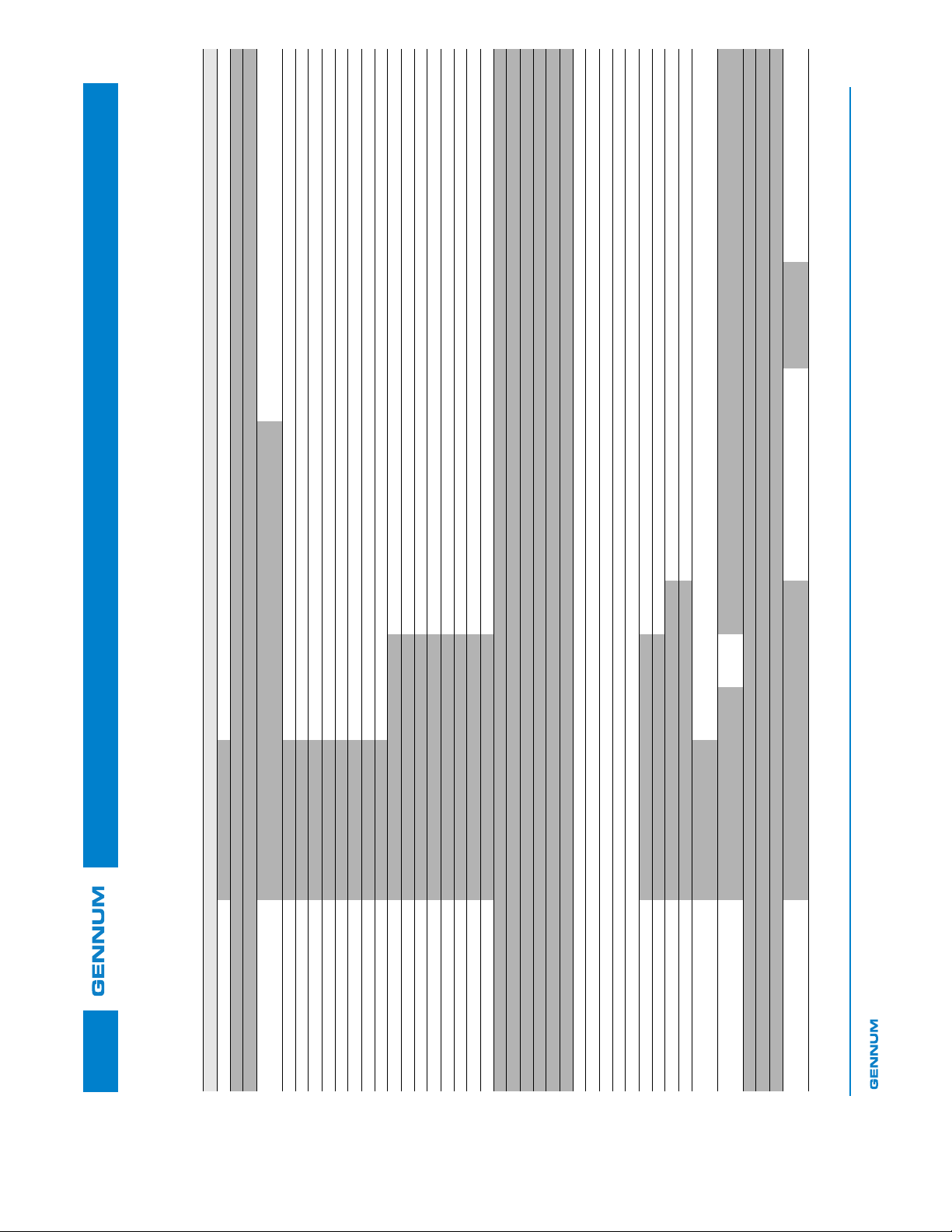
2.5.1 Host Interface Map (R/W registers)
Table 2-5: Host Interface Map (R/W registers)
FIFO_LD_POSITION [12:0] 28h
Register Name Address 15 14 13 12 11 10 9 8 7 6 5 4 3 2 1 0
FF_PIXEL_END_F1[12:0] 24h
FF_PIXEL_START_F1[12:0] 23h
FF_PIXEL_END_F0[12:0] 22h
FF_PIXEL_START_F0[12:0] 21h
AP_PIXEL_END_F1[12:0] 20h
ERROR_MASK_REGISTER 25h VD_STD_
AP_PIXEL_START_F1[12:0] 1Fh
FF_LINE_START_F1[10:0] 1Bh
FF_LINE_END_F0[10:0] 1Ah
FF_LINE_START_F0[10:0] 19h
AP_LINE_END_F1[10:0] 18 h
AP_LINE_START_F1[10:0] 17h
AP_LINE_END_F0[10:0] 16 h
AP_PIXEL_END_F0[12:0] 1Eh
AP_PIXEL_START_F0[12:0] 1Dh
FF_LINE_END_F1[10:0] 1Ch
AP_LINE_START_F0[10:0] 15h
ANC_TYPE(5)[15: 0] 0Eh b15 b14 b13 b12 b 11 b10 b9 b8 b7 b6 b5 b4 b3 b2 b1 b0
ANC_TYPE(4)[15: 0] 0Dh b15 b14 b13 b12 b11 b10 b9 b8 b7 b6 b5 b4 b3 b2 b1 b0
ANC_TYPE(3)[15: 0] 0Ch b15 b14 b13 b12 b11 b10 b9 b8 b7 b6 b5 b4 b3 b2 b1 b0
ANC_TYPE(2)[15: 0] 0Bh b15 b14 b13 b12 b11 b10 b9 b8 b7 b6 b5 b4 b3 b2 b1 b0
ANC_TYPE(1)[15: 0] 0Ah b15 b14 b13 b12 b11 b10 b9 b8 b7 b6 b5 b4 b3 b2 b1 b0
FIFO_EMPTY_OFFSET 06h
IO_CONFIG 05h
ANC_LINE_A[10:0] 08h
FIFO_FULL_OFFSET 07h
ANC_LINE_B[10:0] 09h
DATA_FORMAT 04h
NOTE: Addresses 02Ch to 42Bh store the contents of the internal FIFO. The contents may be accessed in Ancillary Data Extraction mode (see
IOPROC_DISABLE 00h ANC_PKT_EX
DATA_
FORMAT
b0
GS9090 Data Sheet
DATA_
FORMAT
b1
DATA_
FORMAT
b2
CCS_ERR SAV_ERR EAV_ERR
DATA_
FORMAT
b3
LOCK_
ERR
STD_
LOCK
VERSION_35
2M
DETECT
AP_CRC_
ERR
FF_CRC_
ERR
VD_STD_
ERR
FF-UES_IN FF-IDA_IN FF-IDH_IN FF-EDA_IN FF-EDH_IN AP-UES_IN AP-IDA_IN AP-IDH_IN AP-EDA_IN AP-EDH_IN
).
19 of 70
b10b9b8b7b6b5b4b3b2b1b0
b12b11b10b9b8b7b6b5b4b3b2b1 b0
b12b11b10b9b8b7b6b5b4b3b2b1 b0
ANC-EDH
ANC-EDA
ANC-IDH
ANC-IDA
_IN
Section 3.10.3
_IN
_IN
_IN
_IN
28201 - 1 July 2005
Not Used ANC-UES ANC-IDA ANC-IDH ANC-EDA ANC-EDH FF-UES FF-IDA FF-IDH FF-EDA FF-EDH AP-UES AP-IDA AP-IDH AP-EDA AP-EDH
Not Used ANC-UES
28h
27h
26h
25h
24h
23h
22h
21h
20h
1Fh
1Eh
1Dh
1Ch
1Bh
1Ah
19h
18h
17h
16h
15h
0Eh
0Dh
0Ch
0Bh
0Ah
09h
08h
07h
06h
05h
00h
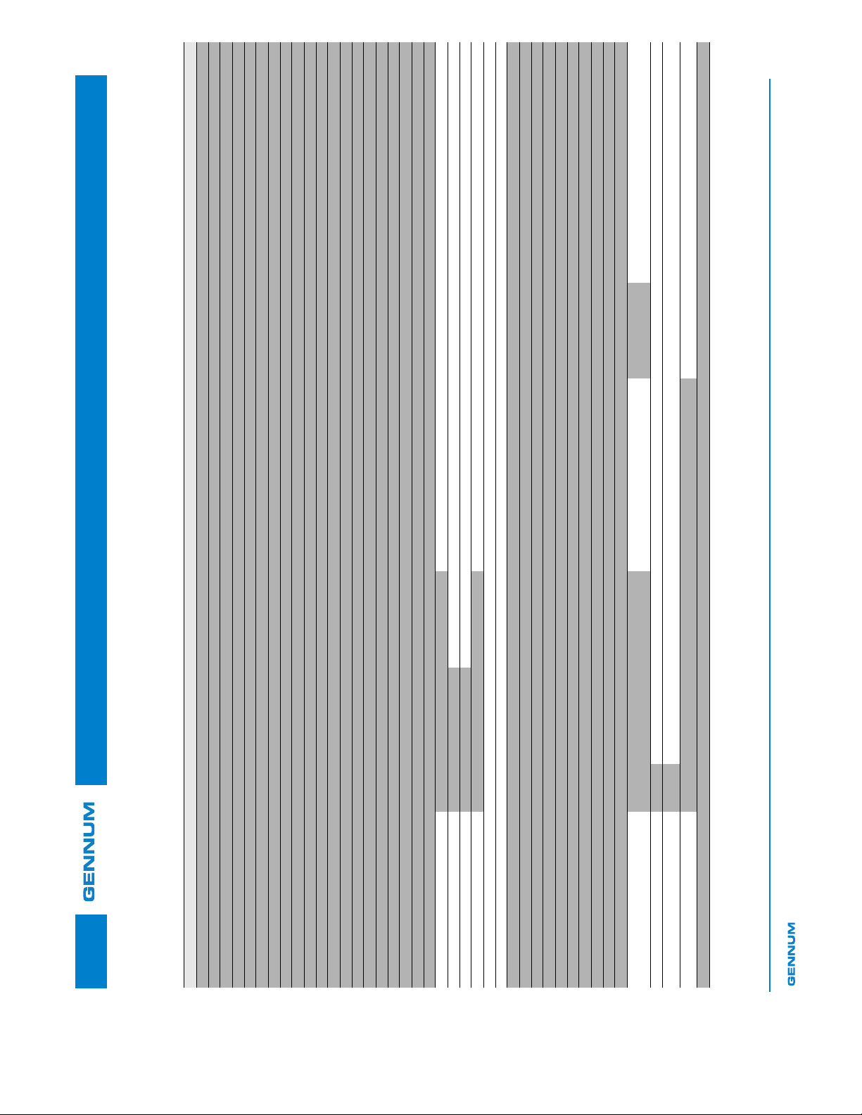
2.5.2 Host Interface Map (Read only registers)
Table 2-6: Host Interface Map (Read only registers)
RASTER_STRUCTURE3[12:0] 13h
VIDEO_FORMAT_OUT_B(4,3) 10h VFO4-b7 VFO4-b6 VFO4-b5 VFO4-b4 VFO4-b3 VFO4-b2 VFO4-b1 VFO4-b0 VFO3-b7 VFO3-b6 VFO3-b5 VFO3-b4 VFO3-b3 VFO3-b2 VFO3-b1 VFO3-b0
VIDEO_FORMAT_OUT_A(2,1) 0Fh VFO2-b7 VFO2-b6 VFO2-b5 VFO2-b4 VFO2-b3 VFO2-b2 VFO2-b1 VFO2-b0 VFO1-b7 VFO1-b6 VFO1-b5 VFO1-b4 VFO1-b3 VFO1-b2 VFO1-b1 VFO1-b0
RASTER_STRUCTURE2[12:0] 12h
Register Name Address 15 14 13 12 11 10 9 8 7 6 5 4 3 2 1 0
RASTER_STRUCTURE1[10:0] 11h
RASTER_STRUCTURE4[10:0] 14h b10b9b8b7b6b5b4b3b2b1b0
EDH_FLAG_OUT 03h
ERROR_STATUS 01h
EDH_FLAG_IN 02h
DATA_FORMAT 04h AP_CRC_V FF_CRC_V EDH_
NOTE: Addresses 02Ch to 42Bh store the contents of the internal FIFO. The contents may be accessed in Ancillary Data Extraction mode (see

3. Detailed Description
• Functional Overview on page 20
• Serial Digital Input on page 21
• Clock and Data Recovery on page 21
• Serial-To-Parallel Conversion on page 21
• Modes Of Operation on page 22
• SMPTE Functionality on page 25
• DVB-ASI Functionality on page 29
• Data-Through functionality on page 29
• Additional Processing Features on page 30
• Internal FIFO Operation on page 46
• Parallel Data Outputs on page 55
• Programmable Multi-Function Outputs on page 56
• GS9090 Low-latency Mode on page 58
• GSPI Host Interface on page 59
• JTAG Operation on page 63
• Device Power Up on page 64
GS9090 Data Sheet
3.1 Functional Overview
The GS9090 is a 270Mb/s reclocking deserializer with an internal FIFO and
programmable multi-function output port. The device has two basic modes of
operation which determine precisely how SMPTE or DVB-ASI compliant input data
streams are reclocked and processed.
In Auto mode (AUTO/MAN
deserialize, and process SD SMPTE 259M-C, or DVB-ASI input data.
In Manual mode (AUTO/MAN
device pins for the correct reception of either SMPTE or DVB-ASI data. Manual
mode also supports the reclocking and deserializing of 270Mb/s data not
conforming to SMPTE or DVB-ASI streams.
The digital signal processing core implements several data processing functions
including error detection and correction and automatic video standards detection.
These features are all enabled by default, but may be individually disabled via
internal registers accessible through the GSPI host interface.
The provided programmable multi-function output pins may be configured to output
various status signals including H, V, and F timing, ancillary data detection, EDH
detection, and a FIFO load pulse. The internal FIFO supports 4 modes of
operation, which may be used for data alignment / delay, MPEG packet extraction,
or ancillary data extraction.
= HIGH), the GS9090 will automatically detect, reclock,
= LOW), the application layer must set external
The GS9090 contains a JTAG interface for boundary scan test implementations.
28201 - 1 July 2005 20 of 70

3.2 Serial Digital Input
The GS9090 contains a current mode differential serial digital input buffer, allowing
the device to be connected to SMPTE 259M-C compliant serial digital input signals.
The input buffer has internal 50Ω termination resistors, which are connected to
ground via the TERM pin. If the input signal is AC coupled to the device, the signal
source common mode level will be set internally to approximately 1.45V.
3.3 Clock and Data Recovery
The output of the serial digital input buffer passes to the GS9090's internal
reclocker block. The function of this block is to lock to the input data stream, extract
a clean clock, and retime the serial digital data to remove high frequency jitter.
The operating centre frequency of the internal reclocker is 270Mb/s where the input
jitter tolerance (IJT) is +/- 0.2UI at this rate.
If the reclocker locks to the signal, it will provide internal pll_lock and carrier_detect
signals to the lock detect block of the device.
GS9090 Data Sheet
3.3.1 Internal VCO and Phase Detector
The GS9090 uses an internal VCO and PFD as part of the internal reclocker's
phase-locked loop. Each block requires a +1.8V DC power supply, which is
supplied via the VCO_VDD / VCO_GND and PLL_VDD / PLL_GND pins.
3.4 Serial-To-Parallel Conversion
The retimed data and phase-locked clock signals from the internal reclocker are
fed to the serial-to-parallel converter. The function of this block is to extract 10-bit
parallel data words from the reclocked serial data stream and simultaneously
present them to the SMPTE and DVB-ASI word alignment blocks.
28201 - 1 July 2005 21 of 70
 Loading...