

Page 1
查询GS9025A供应商
™
GS9025A
GENLINX
II
Serial Digital Receiver
PRELIMINARY DATA SHEET
FEATURES
• SMPTE 259M compliant
• operational to 540Mb/s
• automatic cable equalization (typically greater than
350m of high quality cable at 270Mb/s)
• adjustment-free operation
• auto-rate selection (5 rates) with manual override
• single external VCO resistor for operation with five
input data rates
• data rate indication output
• serial data outputs muted and serial clock remains
active when input data is lost
• operation independent of SAV/EAV sync signals
• signal strength indicator output
• carrier detect with programmable threshold level
• power savings mode (output serial clock disable)
APPLICATIONS
Cable equalization plus clock and data recovery for all high
speed serial digital interface applications involving SMPTE
259M and other data standards.
DESCRIPTION
The GS9025A provides automatic cable equalization and
high performance clock and data recovery for serial digital
signals. The GS9025A receives either single-ended or
differential serial digital data and outputs differential clock
and retimed data signals at PECL levels (800mV). The onboard cable equalizer provides up to 40dB of gain at
200MHz which typically results in equalization of greater
than 350m of high quality cable at 270Mb/s.
The GS9025A operates in either auto or manual data rate
selection mode. In both modes, the GS9025A requires only
one external resistor to set the VCO centre frequency and
provides adjustment free operation.
The GS9025A has dedicated pins to indicate signal
strength/carrier detect, LOCK and data rate. Optional
external resistors allow the carrier detect threshold level to
be customized to the user's requirement. In addition, the
GS9025A provides an 'Output Eye Monitor Test'
(OEM_TEST) for diagnostic testing of signal integrity after
equalization, prior to reslicing. The serial clock outputs can
also be disabled to reduce power. The GS9025A operates
from a single +5 or -5 volt supply.
ORDERING INFORMATION
PART NUMBER PACKAGE TEMPERATURE
GS9025ACQM 44 pin MQFP Tray 0°C to 70°C
GS9025ACTM 44 pin MQFP Tape 0°C to 70°C
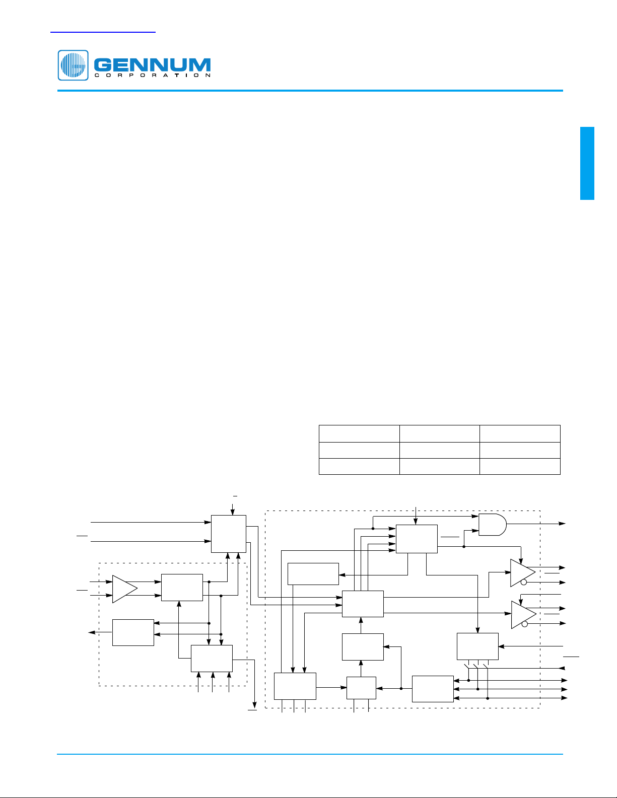
GS9025A
C
OSC
LOGIC
DECODER
MUTE
3 BIT
COUNTER
LOCK
SDO
SDO
CLK_EN
SCO
SCO
SMPTE
AUTO/MAN
SS0
SS1
SS2
DDI
DDI
SDI
SDI
OEM_TEST
+
+
-
-
EYE
MONITOR
VARIABLE
GAIN EQ
STAGE
AUTO EQ
CONTROL
+ -
AGC CAP CD_ADJ
A/D
ANALOG
DIGITAL
MUX
SSI/CD
CARRIER DETECT
PHASELOCK
HARMONIC
FREQUENCY
ACQUISITION
PHASE
DETECTOR
DIVISION
CHARGE
PUMP
LF+ LFS LF- CBG R
VCO
VCO
BLOCK DIAGRAM
Revision Date: June 2000 Document No. 522 - 75 - 00
GENNUM CORPORATION P.O. Box 489, Stn. A, Burlington, Ontario, Canada L7R 3Y3
Tel. +1 (905) 632-2996 Fax. +1 (905) 632-5946 E-mail: info@gennum.com
www.gennum.com
Page 2
ABSOLUTE MAXIMUM RATINGS
PARAMETER VALUE
Supply Voltage (V
Input Voltage Range (any input) V
Operating Temperature Range 0°C ≤ T
Storage Temperature Range -65°C ≤ T
)5.5V
S
+ 0.5 to V
CC
- 0.5V
EE
≤ 70°C
A
≤ 150°C
S
Lead Temperature (soldering, 10 sec) 260°C
DC ELECTRICAL CHARACTERISTICS
VCC = 5.0V, TA = 25°C unless otherwise stated, RLF = 1.8k, C
PARAMETER CONDITION MIN
Supply Voltage 4.75 5 5.25 V 1
Supply Current CLK_EN = 0 - 115 mA 1
CLK_EN = 1 - 125
SDI Common Mode Voltage - 2.5 - V 1
DDI Common Mode Input
Voltage Range
DDI Differential Input Drive 200 800 2000 mV 1
SSI/CD
Output Current Source,
= 50pF,
C
LMAX
R
= open cct.
L
= 15nF, C
LF1
V
EE
= 3.3pF
LF2
TYPICAL
+(V
/2) 0.4 to 4.6 VCC-(V
DIFF
1
MAX UNITS NOTES
/2) V 2 1
DIFF
- - 18 µA 3
GS9025A
TEST
LEVEL
Source,
C
LMAX
R
=5K
L
= 50pF,
- - 110 µA 3
Sink - 1.0 1.5 mA 3
AGC Common Mode Voltage - 2.7 - V 1
OEM_TEST Bias Potential - 4.5 - V 5 1
A/D
, AUTO/MAN, SMPTE,
High 2.0 - - V 1
SS[2:0] Input Voltage
Low - - 0.8
CLK_EN Input Voltage High 2.5 - - V 1
Low - - 0.8
LOCK Output Sink Current 500 - - µA 3 1
SS[2:0] Output Voltage High 4.4 4.7 - V 1
Low - 0.2 0.4
SS[2:0] Source Current Auto Mode 180 300 - µA 1
SS[2:0] Sink Current Auto Mode 0.6 1.0 - mA
SS[2:0] Source Current Manual Mode - 0 - µA 4 1
GENNUM CORPORATION
2
522 - 75 - 00
Page 3
DC ELECTRICAL CHARACTERISTICS (continued)
VCC = 5.0V, TA = 25°C unless otherwise stated, RLF = 1.8k, C
= 15nF, C
LF1
= 3.3pF
LF2
PARAMETER CONDITION MIN
TYPICAL
1
MAX UNITS NOTES
SS[2:0] Sink Current Manual Mode - 0.8 5 µA
CLK_EN Source Current Low - 26 55 µA 1
NOTES
1. TYPICAL - measured on EB9025A board.
is the differential input signal swing.
2. V
DIFF
3. LOCK is an open collector output and requires an external pullup
resistor.
4. Pins SS[2:0] are outputs in AUTO mode and inputs in MANUAL
mode.
5. If OEM_TEST is permanently enabled, operating temperature
range is limited from 0°C to 60°C inclusive.
TEST LEVELS
1. Production test at room temperature and nominal supply
voltage with guardbands for supply and temperature
ranges.
2. Production test at room temperature and nominal supply
voltage with guardbands for supply and temperature
ranges using correlated test.
3. Production test at room temperature and nominal supply
voltage.
4. QA sample test.
5. Calculated result based on Level 1,2, or 3.
6. Not tested. Guaranteed by design simulations.
7. Not tested. Based on characterization of nominal parts.
8. Not tested. Based on existing design/characterization
data of similar product.
AC ELECTRICAL CHARACTERISTICS
VCC = 5.0V, VEE = 0V, TA = 25°C unless otherwise stated, RLF = 1.8k, C
PARAMETER CONDITIONS MIN
= 15nF, C
LF1
= 3.3pF
LF2
TYPICAL
1
MAX UNITS NOTES
TEST
LEVEL
GS9025A
TEST
LEVEL
Serial Data Rate SDI 143 - 540 Mb/s 1
Maximum Equalizer Gain @ 200MHz - 40 - dB 7
Additive Jitter
[Pseudorandom (2
23
-1)]
270Mb/s, 300m
(Belden 8281)
540Mb/s, 100m
- 300 - ps p-p 2, 8 3
- 275 -
(Belden 8281)
Intrinsic Jitter
23
[Pseudorandom (2
-1)]
Intrinsic Jitter
[Pathological (SDI checkfield)]
270Mb/s - 185 see Figure 12 ps p-p 2, 7 4
540Mb/s - 164
270Mb/s - 462 see Figure 13 ps p-p 2, 7 1
360Mb/s - 308
540Mb/s - 260
Input Jitter Tolerance 270Mb/s 0.40 0.56 - UI p-p 3, 7 1
540Mb/s 0.35 0.43 -
Lock Time Synchronous Switch
Lock Time Asynchronous Switch
t
< 0.5µs, 270Mb/s - 1 - µs 4 7
switch
0.5µs< t
t
switch
Loop Bandwidth
<10ms - 1 - ms
switch
> 10 ms - 4 - ms
-10 - ms57
= 6MHz @ 540Mb/s
Carrier Loss Time 0.5 1 2 µs 6 7
SDO to SCO Synchronization -200 0 200 ps 7
3
GENNUM CORPORATION
522 - 75 - 00
Page 4
AC ELECTRICAL CHARACTERISTICS
VCC = 5.0V, VEE = 0V, TA = 25°C unless otherwise stated, RLF = 1.8k, C
= 15nF, C
LF1
= 3.3pF
LF2
PARAMETER CONDITIONS MIN
SDO, SCO Output Signal
TYPICAL
1
MAX UNITS NOTES
75Ω DC load 600 800 1000 mV p-p 1
TEST
LEVEL
Swing
SDO, SCO Rise & Fall times 20%-80% 200 300 400 ps 7
SDI/SDI
Input Resistance - 10 - k
SDI/SDI
Input Capacitance - 1.0 - pF 8 6
SDI/SDI
Input Return Loss at 270MHz 15 20 - dB 8 6
Carrier Detect Response Time Carrier Applied,
<50pF, RL=open cct.
C
L
Carrier Removed,
C
<50pF, RL=open cct.
L
NOTES
1. TYPICAL - measured on EB9025A board.
2. Characterized 6 sigma rms.
3. IJT measured with sinusoidal modulation beyond Loop
Bandwidth (at 6.5MHz).
4. Synchronous switching refers to switching the input data from
one source to another source which is at the same data rate (ie.
line 10 switching for component NTSC).
5. Asynchronous switching refers to switching the input data from
one source to another source which is at a different data rate.
6. Carrier Loss Time refers to the response of the SDO output from
valid re-clocked input data to mute mode when the input signal
is removed.
7. Using the DDI input, A/D
8. Using the SDI input, A/D
=0.
=1.
-3 - µs86
-30 -
TEST LEVELS
1. Production test at room temperature and nominal supply
voltage with guardbands for supply and temperature
ranges.
2. Production test at room temperature and nominal supply
voltage with guardbands for supply and temperature ranges
using correlated test.
3. Production test at room temperature and nominal supply
voltage.
4. QA sample test.
5. Calculated result based on Level 1,2, or 3.
6. Not tested. Guaranteed by design simulations.
7. Not tested. Based on characterization of nominal parts.
8. Not tested. Based on existing design/characterization data
of similar product.
Ω
86
GS9025A
TEKTRONIX
GigaBERT
TRANSMITTER
GENNUM CORPORATION
1400
DATA
DATA
CLOCK
BELDEN 8281
GS9028
CABLE
DRIVER
CABLE
Fig. 1 Test Setup for Figures 6 - 13
4
EB9025A
BOARD
TEKTRONIX
GigaBERT
1400
ANALYZER
TRIGGER
522 - 75 - 00
Page 5
PIN CONNECTIONS
DDI
DDI
V
_75
CC
V
CC
V
SDI
SDI
V
V
CD_ADJ
AGC-
EE
CC
EE
LFS
OSC
LOCK
C
EE
LF-
V
EE
V
_RTN
R
_75
CC
OEM_TEST
SMPTE
A/D
V
EE
SSI/CD
GS9025A
TOP VIEW
LF+
V
44 43 42 41 40 39 38 37 36 35 34
1
2
3
4
5
6
7
8
9
10
11
12 13 14 15 16 17 18 19 20 21 22
CC
V
AGC+
CLK_EN
R
VCO
VCO
CC
V
CBG
EE
V
GS9025A
33
32
31
30
29
28
27
26
25
24
23
CC
V
V
EE
SDO
SDO
V
EE
SCO
SCO
V
EE
AUTO/MAN
SS0
SS1
SS2
PIN DESCRIPTIONS
NUMBER SYMBOL TYPE DESCRIPTION
1, 2 DDI/DDI
3, 44 V
4, 8, 13, 22, 35 V
5, 9, 14, 18, 27,
_75 I Power supply connection for internal 75Ω pullup resistors connected to DDI/DDI.
CC
CC
V
EE
30, 33, 34, 37
6, 7 SDI/SDI
10 CD_ADJ I Carrier detect threshold adjust.
11, 12 AGC-, AGC+ I External AGC capacitor.
15 LF+ I Loop filter component connection.
16 LFS I Loop filter component connection.
17 LF- I Loop filter component connection.
19 R
20 R
_RTN I Frequency setting resistor return connection.
VCO
VCO
21 CBG I Internal bandgap voltage filter capacitor.
23, 24, 25 SS[2:0] I/O Data rate indication (auto mode) or data rate select (manual mode). TTL/CMOS
I Digital data inputs (Differential ECL/PECL).
I Most positive power supply connection.
I Most negative power supply connection.
I Differential analog data inputs.
I Frequency setting resistor connection.
compatible I/O. In auto mode, these pins can be left unconnected.
26 AUTO/MAN
GENNUM CORPORATION
I Auto or manual mode select. TTL/CMOS compatible input.
5
522 - 75 - 00
Page 6
PIN DESCRIPTIONS (continued)
NUMBER SYMBOL TYPE DESCRIPTION
28, 29 SCO/SCO O Serial clock output. SCO/SCO are differential current mode outputs and require
31, 32 SDO/SDO
36 CLK_EN I Clock enable. When HIGH, the serial clock outputs are enabled.
38 COSC I Timing control capacitor for internal system clock.
39 LOCK O Lock indication. When HIGH, the GS9025A is locked. LOCK is an open collector output
40 SSI/CD
41 A/D
42 SMPTE I SMPTE/Other data rate select. TTL/CMOS compatible input.
43 OEM_TEST O Output ‘Eye’ monitor test. Single-ended current mode output that requires an external
external 75Ω pullup resistors.
O Equalized and reclocked serial digital data outputs. SDO/SDO are differential current
mode outputs and require external 75Ω pullup resistors.
and requires an external 10kΩ pullup resistor.
O Signal strength indicator/Carrier detect.
I Analog/Digital select.
50Ω pullup resistor. This feature is recommended for debugging purposes only. If
enabled during normal operation, the maximum operating temperature is rated to
60°C.
GS9025A
GENNUM CORPORATION
6
522 - 75 - 00
Page 7

TYPICAL PERFORMANCE CURVES
(V
= 5V, TA = 25°C unless otherwise shown)
S
j1
5.00
4.50
4.00
3.50
3.00
SSI/CD OUTPUT VOLTAGE (V)
2.50
0 50 100 150 200 250 300 350 400 450 500
CABLE LENGTH (m)
Fig. 2 SSI/CD Voltage vs. Cable Length
(Belden 8281) (CD_ADJ = 0V)
50
45
40
35
30
25
20
GAIN (dB)
15
10
5
0
1 10 100 1000
FREQUENCY (MHz)
j0.5
j0.2
3000
-j0.2
1620
-j0.5
-j1
Frequencies in MHz, impedances normalized to 50Ω
Fig. 5 Input Impedance
450
400
350
300
250
200
150
JITTER (ps p-p)
100
50
0
0 50 100 150 200 250 300 350 400
(Characterized)
CABLE LENGTH (m)
-j2
540Mb/s
270Mb/s
j2
j5
270
GS9025A
-j5
810
Fig. 3 Equalizer Gain vs. Frequency
5.0
4.5
4.0
3.5
3.0
CD_ADJ VOLTAGE (V)
2.5
2.0
200 250 300 350 400
CABLE LENGTH (m)
Fig. 4 Carrier Detect Adjust Voltage Threshold Characteristics
GENNUM CORPORATION
Fig. 6 Typical Additive Jitter vs. Input Cable Length (Belden 8281)
23
-1)
450
400
350
300
250
CABLE LENGTH (m)
200
150
100
200 300 400 500 600
Pseudorandom (2
DATA RATE (Mb/s)
Fig. 7 Typical Error Free Cable Length
7
522 - 75 - 00
Page 8

GS9025A
Fig. 8 Intrinsic Jitter (223 - 1 Pattern) 30Mb/s
Fig. 9 Intrinsic Jitter (2
23
- 1 Pattern) 143Mb/s
Fig. 11 Intrinsic Jitter (2
2000
1800
1600
1400
1200
1000
800
JITTER (ps)
600
Typical Range, Characterized
400
200
0
100 200 300 400 500 600
23
- 1 Pattern) 540Mb/s
QA Output Jitter Limit, Sample Tested
SDI DATA RATE (Mb/s)
T
=0 to 70˚C, VCC=4.75 to 5.25V for the typical range
A
Fig. 12 Intrinsic Jitter - P seudorandom (2
2000
1800
1600
1400
1200
1000
800
600
JITTER (ps p-p)
400
200
Typical
Typical Range, Characterized
0
100 200 300 400 500 600
= 0 to 70˚C, VCC = 4.75 to 5.25V for the typical range
T
A
QA Output Jitter Limit, Sample Tested
Max
Min
SDI DATA RATE (Mb/s)
Max
Typical
Min
23
- 1)
Fig. 10 Intrinsic Jitter (2
GENNUM CORPORATION
23
- 1 Pattern) 270Mb/s
Fig. 13 Intrinsic Jitter - Pathological SDI Checkfield
8
522 - 75 - 00
Page 9

0.6
0
1
2
3
4
5
50
100
150 200 250 300 350 400 450
500
SSI/CD OUTPUT VOLTAGE (V)
CABLE LENGTH (m)
0
CD_ADJ
CONTROL RANGE
0.5
0.4
0.3
IJT (UI)
0.2
0.1
0
100 200 300 400 500 600
DATA RATE (Mb/s)
TA = 0 to 70˚C, V
= 4.75 to 5.25V
CC
Fig. 14 Typical Input Jitter Tolerance (Characterized)
0.600
0.550
0.500
0.450
143Mb/s
177Mb/s
270Mb/s
360Mb/s
signal passes through a variable gain equalizing stage
whose frequency response closely matches the inverse
cable loss characteristic. In addition, the variation of the
frequency response with control voltage imitates the
variation of the inverse cable loss characteristic with cable
length. The gain stage provides up to 40dB of gain at
200MHz which typically results in equalization of greater
than 350m at 270Mb/s of Belden 8281 cable.
The edge energy of the equalized signal is monitored by a
detector circuit which produces an error signal
corresponding to the difference between the desired edge
energy and the actual edge energy. This error signal is
integrated by an external differential AGC filter capacitor
(AGC+/AGC-) providing a steady control voltage for the
gain stage. As the frequency response of the gain stage is
automatically varied by the application of negative
feedback, the edge energy of the equalized signal is kept
at a constant level which is representative of the original
edge energy at the transmitter.
The equalized signal is also DC restored, effectively
restoring the logic threshold of the equalized signal to its
corrective level irrespective of shifts due to AC coupling.
GS9025A
0.400
0.350
IJT (UI)
0.300
0.250
0.200
0 10203040506070
TEMPERATURE (C˚)
540Mb/s
1-1. Signal Strength Indic a tion/carrier Detect
The GS9025A incorporates an analog signal strength
indicator/carrier detect (SSI/CD
) output indicating both the
presence of a carrier and the amount of equalization
applied to the signal. The voltage output of this pin versus
cable length (signal strength) is shown in Figure 2 and
Figure 16.
With 0m of cable (800mV input signal levels), the SSI/CD
output voltage is approximately 4.5V. As the cable length
Fig. 15 Typical IJT vs. Temperature (V
DETAILED DESCRIPTION
= 5.0V) (Characterized)
CC
increases, the SSI/CD
voltage decreases linearly providing
accurate correlation between the SSI/CD
length.
voltage and cable
The GS9025A Serial Digital Receiver is a bipolar integrated
circuit containing a built-in cable equalizer and reclocker.
Serial digital signals are applied to either the analog
SDI/SDI
SDI/SDI
multiplexer. Signals applied to the DDI/DDI
or digital DDI/DDI inputs. Signals applied to the
inputs are equalized and then passed to a
inputs bypass
the equalizer and go directly to the multiplexer. The
analog/digital select pin (A/D
) determines which signal is
then passed to the reclocker.
Packaged in a 44 pin MQFP, the receiver operates from a
single 5V supply to data rates of 540Mb/s. Typical power
consumption is 575mW.
1. CABLE EQUALIZER
The automatic cable equalizer is designed to equalize
serial digital data signals from 143Mb/s to 540Mb/s.
The serial data signal is connected to the input pins
(SDI/SDI
GENNUM CORPORATION
) either differentially or single-ended. The input
Fig. 16 SSI/CD Voltage vs. Cable Length
When the signal strength decreases to the level set at the
"Carrier Detect Threshold Adjust" pin, the SSI/CD
goes to a logic "0" state (0.8 V) and can be used to drive
9
522 - 75 - 00
voltage
Page 10

other TTL/CMOS compatible logic inputs. In addition, when
loss of carrier is detected, the SDO/SDO
outputs are muted
(set to a known static state).
1-2. Carrier Detect Threshold Adjust
This feature has been designed for use in applications such
as routers where signal crosstalk and circuit noise cause
the equalizer to output erroneous data when no input signal
is present. The use of a Carrier Detect function with a fixed
internal reference does not solve this problem since the
signal to noise ratio on the circuit board could be
significantly less than the default signal detection level set
by the on chip reference. To alleviate this problem, the
GS9025A provides a user adjustable threshold to meet the
unique conditions that exist in each user's application.
Override and internal default settings have also been
provided to give the user total flexibility.
The threshold level at which loss of carrier is detected is
adjustable via external resistors at the CD_ADJ pin. The
control voltage at the CD_ADJ pin is set by a simple resistor
divider circuit (
see Typical Application Circuit
). The
threshold level is adjustable from 200m to 350m. By default
(no external resistors), the threshold is typically 320m. In
noisy environments, it is not recommended to leave this pin
floating. Connecting this pin to V
disables the SDO/SDO
EE
muting function and allows for maximum possible cable
length equalization.
SDO
SCO
Fig. 17 Output and Clock Signal Timing
50%
The reclocker contains four main functional blocks: the
Phase Locked Loop, Auto/Manual Data Rate Select,
Frequency Acquisition, and Logic Circuit.
2-1. Phase Locked Loop (PLL)
The Phase Locked Loop locks the internal PLL clock to the
incoming data rate. A simplified block diagram of the PLL is
shown below. The main components are the VCO, the
phase detector, the charge pump, and the loop filter.
DDI/DDI
2
PHASE
DETECTOR
INTERNAL
PLL CLOCK
GS9025A
1-3. Output Eye Monitor Test
The GS9025A also provides an 'Output Eye Monitor Test'
(OEM_TEST) which allows the verification of signal integrity
after equalization, prior to reslicing. The OEM_TEST pin is
an open collector current output that requires an external
50Ω pullup resistor. When the pullup resistor is not used,
the OEM_TEST block is disabled and the internal
OEM_TEST circuit is powered down. The OEM_TEST
provides a 100mVp-p
signal when driving a 50Ω
oscilloscope input. Due to additional power consumed by
this diagnostic circuit, it is not recommended for continuous
operation.
2. RECLOCKER
The reclocker receives a differential serial data stream from
the internal multiplexer. It locks an internal clock to the
incoming data. It outputs the differential PECL retimed data
signal on SDO/SDO
SCO
. The timing between the output and clock signals is
. It outputs the recovered clock on SCO/
shown in Figure 17.
DIVISION
LF+
2-2. VCO
CHARGE
PUMP
LFS
LF-
RLFC
LF1
C
LF2
Fig. 18 Simplified Block Diagram of the PLL
LOOP
FILTER
VCO
R
VCO
The VCO is a differential low phase noise, factory trimmed
design that provides increased immunity to PCB noise and
precise control of the VCO centre frequency. The VCO
operates between 30 and 540Mb/s and has a pull range of
±15% about the centre frequency. A single low impedance
external resistor, R
Figure 19
). The low impedance R
, sets the VCO centre frequency (
VCO
minimizes thermal
VCO
see
noise and reduces the PLL's sensitivity to PCB noise.
For a given R
value, the VCO can oscillate at one of two
VCO
frequencies. When SMPTE = SS0 = logic 1, the VCO centre
frequency corresponds to the ƒ
curve. For all other
L
SMPTE/SS0 combinations, the VCO centre frequency
corresponds to the ƒ
curve (ƒ
H
is approximately 1.5 x ƒL).
H
GENNUM CORPORATION
10
522 - 75 - 00
Page 11

800
700
600
500
400
300
200
VCO FREQUENCY (MHz)
100
0
0 200 400 600 800 1000 1200 1400 1600 1800
Fig. 19 R
The recommended R
ƒ
H
ƒ
L
SMPTE=1
SSO=1
R
(Ω)
VCO
vs. VCO Centre Frequency
VCO
value for auto rate SMPTE 259M
VCO
applications is 365Ω.
The VCO and an internal divider generate the PLL clock.
Divider moduli of 1, 2, and 4 allow the PLL to lock to data
rates from 143Mb/s to 540Mb/s. The divider modulus is set
by the AUTO/MAN
details, see section 4, Auto/Manual Data Rate Select)
, SMPTE, and SS[2:0] pins
(for further
. In
addition, a manually selectable modulus 8 divider allows
operation at data rates as low as 30Mb/s.
When the input data stream is removed for an excessive
period of time
(see AC electrical characteristics table),
the
VCO frequency can drift from the previously locked
frequency to the limits shown in Table1.
TABLE 1: Frequency Drift Range (when PLL loses lock)
for SMPTE 259M applications where pathological signals
have data transition densities of 0.05.
2-5. Loop Filter
The loop filter integrates the charge pump packets and
produces a VCO control voltage. The loop filter is
comprised of three external components which are
connected to pins LF+, LFS, and LF-. The loop filter design
is fully differential giving the GS9025A increased immunity
to PCB board noise.
The loop filter components are critical in determining the
loop bandwidth and damping of the PLL. Choosing these
component values is discussed in detail in the PLL DESIGN
GUIDELINES section. Recommended values for
SMPTE259M applications are shown in the Typical
Application Circuit.
3. FREQUENCY ACQUISITION
The core PLL is able to lock if the incoming data rate and
the PLL clock frequency are within the PLL capture range
(which is slightly larger than the loop bandwidth). To assist
the PLL to lock to data rates outside of the capture range,
the GS9025A uses a frequency acquisition circuit.
The frequency acquisition circuit sweeps the VCO control
voltage so that the VCO frequency changes from -10% to
+10% of the centre frequency. Figure 20 shows a typical
sweep waveform.
t
swp
t
sys
GS9025A
LOSES LOCK FROM MIN (%) MAX(%)
143Mb/s lock -21 21
177Mb/s lock -12 26
270Mb/s lock -13 28
360 Mb/s lock -13 24
540 Mb/s lock -13 28
2-3. Phase Detector
The phase detector compares the phase of the PLL clock
with the phase of the incoming data signal and generates
error correcting timing pulses. The phase detector design
provides a linear transfer function which maximizes the
input jitter tolerance of the PLL.
2-4. Charge Pump
The charge pump takes the phase detector output timing
pulses and creates a charge packet that is proportional to
the system phase error. A unique differential charge pump
design insures that the output phase does not drift when
data transitions are sparse. This makes the GS9025A ideal
V
LF
A
T
cycle
= t
T
cycle
Fig. 20 Typical Sweep Waveform
+ t
swp
sys
The VCO frequency starts at point A and sweeps up
attempting to lock. If lock is not established during the up
sweep, the VCO is then swept down. The system is
designed such that the probability of locking within one
cycle period is greater than 0.999. If the system does not
lock within one cycle period, it will attempt to lock in the
subsequent cycle. In manual mode, the divider modulus is
fixed for all cycles. In auto mode, each subsequent cycle is
based on a different divider moduli as determined by the
internal 3-bit counter.
GENNUM CORPORATION
11
522 - 75 - 00
Page 12

The average sweep time, t
filter component, C
, and the charge pump current, Ι
LF1
t
SWP
, is determined by the loop
swp
4C
LF1
----------------=
3I
CP
CP
:
The nominal sweep time is approximately 121µs when
.
= 165µA (R
CP
= 365Ω).
VCO
(see section 3-1,
sys
C
= 15nF and Ι
LF1
An internal system clock determines t
Logic Circuit)
3-1. Logic Circuit
The GS9025A is controlled by a finite state logic circuit
which is clocked by an asynchronous system clock. That is,
the system clock is completely independent of the incoming
data rate. The system clock runs at low frequencies, relative
to the incoming data rate, and thus reduces interference to
the PLL.The period of the system clock is set by the COSC
capacitor and is:
t
9.6 104C
sys
The recommended value for t
OSC
is 450µs (C
sys
ondssec[]××=
= 4.7nF)
OSC
4. AUTO/MANUAL DATA RATE SELECT
The GS9025A can operate in either auto or manual data
rate select mode. The mode of operation is selected by a
single input pin (AUTO/MAN
4-1. Auto Mode (AUTO/MAN = 1)
).
In auto mode, the GS9025A uses a 3-bit counter to
automatically cycle through five (SMPTE=1) or three
(SMPTE=0) different divider moduli as it attempts to acquire
lock. In this mode, the SS[2:0] pins are outputs and indicate
the current value of the divider moduli according Table 2.
NOTE: For SMPTE = 0 and divider moduli of 2 and 4, the
PLL can correctly lock for two values of SS[2:0].
4-2. Manual Mode (AUTO/MAN = 0)
In manual mode, the GS9025A divider moduli is fixed. In
this mode, the SS[2:0] pins are inputs and set the divider
moduli according to Table 3.
5. LOCKING
The GS9025A indicates lock when three conditions are
satisfied:
1. Input data is detected.
2. The incoming data signal and the PLL clock are phase
locked.
3. The system is not locked to a harmonic.
TABLE 2.
AUTO/MAN
, ƒL = VCO centre frequency as per Figure 19.
ƒ
H
= 1 (AUTO MODE)
SMPTE SS[2:0]
DIVIDER
MODULI
1 000 4 ƒ
1 001 2 ƒ
1 010 2 ƒ
1 011 1 ƒ
1 100 1 ƒ
1 101 - -
1 110 - -
1 111 - -
0 000 4 ƒ
0 001 4 ƒ
0 010 2 ƒ
0 011 2 ƒ
0 100 1 ƒ
0 101 - -
0 110 - -
0 111 - -
TABLE 3.
AUTO/MAN
, ƒL = VCO centre frequency as per Figure 19.
ƒ
H
= 1 (MANUAL MODE)
SMPTE SS[2:0]
DIVIDER
MODULI
1 000 4 ƒ
1 001 2 ƒ
1 010 2 ƒ
1 011 1 ƒ
1 100 1 ƒ
1 101 8 ƒL/8
1 110 8 ƒ
1 111 - -
0 000 4 ƒ
0 001 4 ƒ
0 010 2 ƒ
0 011 2 ƒ
0 100 1 ƒ
0 101 1 ƒ
0 110 8 ƒH/8
0 111 - -
PLL CLOCK
/4
H
/2
L
/2
H
L
H
/4
H
/4
H
/2
H
/2
H
H
PLL CLOCK
/4
H
/2
L
/2
H
L
H
/8
H
/4
H
/4
H
/2
H
/2
H
H
H
GS9025A
GENNUM CORPORATION
12
522 - 75 - 00
Page 13

The GS9025A defines the presence of input data when at
least one data transition occurs every 1µs.
The GS9025A assumes that it is NOT locked to a harmonic
if the pattern ‘101’ or ‘010’ (in the reclocked data stream)
occurs at least once every t
/3 seconds. Using the
sys
recommended component values, this corresponds to
approximately 150µs. In a harmonically locked system, all
bit cells are double clocked and the above patterns
become ‘110011’ and ‘001100’, respectively.
5-1. Lock Time
The lock time of the GS9025A depends on whether the
input data is switching synchronously or asynchronously.
Synchronous switching refers to the case where the input
data is changed from one source to another source which is
at the same data rate (but different phase). Asynchronous
switching refers to the case where the input data is
changed from one source to another source which is at a
different data rate.
When input data to the GS9025A is removed, the GS9025A
latches the current state of the counter (divider modulus).
Therefore, when data is reapplied, the GS9025A begins the
lock procedure at the previous locked data rate. As a result,
in synchronous switching applications, the GS9025A locks
very quickly. The nominal lock time depends on the
switching time and is summarized in the Table 4.
TABLE 4.
6. OUTPUT DATA MUTING
The GS9025A internally mutes the SDO and SDO outputs
when the device is not locked. When muted, SDO/SDO
are
latched providing a logic state to the subsequent circuit
and avoiding a condition where noise could be amplified
and appear as data.
The output data muting timing is shown in Figure 21.
DDI
LOCK
SDO
7. CLOCK ENABLE
VALID
DATA
NO DATA TRANSITIONS
OUTPUTS MUTED
Fig. 21 Output Data Muting Timing
VALID
DATA
When CLK_EN is high, the GS9025A SCO/SCO outputs are
enabled. When CLK_EN is low, the SCO/SCO
tri-stated and float to V
. Disabling the clock outputs
CC
outputs are
results in a power savings of 10%. It is recommended that
the CLK_EN input be hard wired to the desired state. For
applications which do not require the clock output, connect
CLK_EN to Ground and connect the SCO/SCO
V
.
CC
outputs to
GS9025A
SWITCHING TIME LOCK TIME
<0.5µs 10µs
0.5µs - 10ms 2t
>10ms 2T
cycle
sys
+ 2t
sys
In asynchronous switching applications, including power
up, the lock time is determined by the frequency acquisition
circuit
(see section 3, Frequency Acquisition Circuit)
.
To acquire lock in manual mode, the frequency acquisition
circuit may have to sweep over an entire cycle depending
on initial conditions. Maximum lock time is 2T
cycle
+ 2t
sys
.
To acquire lock in auto tune mode, the frequency
acquisition circuit may have to cycle through 5 possible
counter states depending on initial conditions. Maximum
lock time is 6T
The nominal value of T
cycle
+ 2t
sys.
for the GS9025A operating in a
cycle
typical SMPTE 259M application is approximately 1.3ms.
The GS9025A has a dedicated LOCK output (pin 39)
indicating when the device is locked. It should be noted
that in synchronous switching applications where the
switching time is less than 0.5µs, the LOCK output will NOT
be de-asserted and the data outputs will NOT be muted.
8. STRESSFULL DATA PATTERNS
All PLL's are susceptible to stressful data patterns which
can introduce bit errors in the data stream. PLL's are most
sensitive to patterns which have long run lengths of 0's or
1's (low data transition densities for a long period of time).
The GS9025A is designed to operate with low data
transition densities such as the SMPTE 259M pathological
signal (data transition density = 0.05).
9. PLL DESIGN GUIDELINES
The reclocking performance of the GS9025A is primarily
determined by the PLL. Thus, it is important that the system
designer is familiar with the basic PLL design equations.
A model of the GS9025A PLL is shown in Figure 22. The
main components are the phase detector, the VCO, and the
external loop filter components.
GENNUM CORPORATION
13
522 - 75 - 00
Page 14

PHASE
WZW
P1
W
BW
W
P2
FREQUENCY
AMPLITUDE
s2C
LF2
Ls
L
R
LF
---------
1++
QR
LF
R
LF2
L
----------- -=
1
R
LF2CLF2
------------------------- -
L
R
LF
-------- -
4>
DETECTOR
Ø
+
i
9-1. Transfer Function
K
PD
-
LOOP
FILTER
Fig. 22 Model of the GS9025A
Ι
CP
R
LF
C
LF1
LF2
C
VCO
2 π K
Ns
ƒ
Ø
o
The transfer function of the PLL is defined as Øo/Øi and can
be approximated as:
ƒ
1+
L
---------–
R
LF
Equation 1
C
LF2
1
---------
Ls
R
L
---------------------------------------------------------
2
1+
s
1++
LF
Ø
o
=
-------
Ø
i
where and
sC
----------------------------------------------------------------
L
LF1RLF
sC
LF1RLF
N
--------------------=
DICPK
Fig. 23 Transfer Function Bode Plot
The 3dB bandwidth of the transfer function is
approximately:
w
w
BW
------------
w
P2
BW
⁄()
w
BWwP2
----------------------------------+
12
–
w
------------
w
w
----------------------------------------------------------------------
3dB
12
–
BW
P2
w
BW
------------
≈=
0.78
2
GS9025A
N is the divider modulus
D is the data density (=0.5 for NRZ data)
is the charge pump current in amps
I
CP
K
is the VCO gain in Hz/V
ƒ
This response has 1 zero (w
(w
P1,wBW,wP2
) where:
w
P1
-----------------------=
w
Z
C
---------------------------------------=
C
LF1RLF
w
BW
---------------------- -=
w
P2
C
) and three poles
Z
1
LF1RLF
1
L
---------–
R
LF
R
LF
---------=
L
1
LF2RLF
The bode plot for this transfer function is plotted in
Figure 23.
9-2. Transfer Function Peaking
There are two causes of peaking in the PLL transfer function
given by Equation 1.
The first is quadratic:
which has:
w
o
1
--------------------=
L
C
LF2
and
This response is critically damped for Q = 0.5.
Thus, to avoid peaking:
C
1
LF2
------------ -
L
---
<
2
or
R
LF
Therefore,
> 4 w
w
P2
BW
To reduce the high frequency content on the loop filter, keep
w
as low as possible.
P2
GENNUM CORPORATION
The second is the zero-pole combination:
s
sC
LF1RLF
----------------------------------------------------------
sC
LF1RLF
1+
1
---------–
R
LF
------- 1+
w
Z
--------------------=
s
---------- 1+
1+
w
P1
14
522 - 75 - 00
Page 15

This causes lift in the transfer function given by:
PHII
PHIO
R2
E1
R
LF
C
LF1
C
LF2
G1
V1
2 π K
ƒ
IN+
IN-
Ns
1
LF
NOTE: PHII, PHIO, LF, and 1 are node names in the SPICE netlist.
20 LOG
w
P1
----------
w
Z
20 LOG
=
1
---------------------
w
----------- -–
1
w
BW
Z
9-4. SPICE Simulations
More detailed analysis of the GS9025A PLL can be done
using SPICE. A SPICE model of the PLL is shown below:
To keep peaking to less than 0.05dB:
< 0.0057w
w
Z
9.3 Selection of Loop Filter Components
BW
Based on the above analysis, the loop filter components
should be selected for a given PLL bandwidth, ƒ
3dB
, as
follows:
1. Calculate
2N
L
---------------=
I
CPKƒ
where:
is the charge pump current and is a function of the
I
CP
resistor and is obtained from Figure 24.
R
VCO
K
= 90MHz/V for VCO frequencies corresponding to
ƒ
curve.
the ƒ
L
K
= 140MHz/V for VCO frequencies corresponding to
ƒ
the ƒH curve.
N is the divider modulus
(ƒL, ƒH and N can be obtained from Table 2 or Table 3)
2. Choose R
3. Choose C
4. Choose C
= 2(3.14)ƒ
LF
= 174L/(RLF)
LF1
= L/4(RLF)
LF2
3dB
2
(0.78)L
2
Fig. 25 SPICE Model of the PLL
The model consists of a voltage controlled current source
(G1), the loop filter components (R
LF
, C
, and C
LF1
LF2
), a
voltage controlled voltage source (E1), and a voltage
source (V1). R2 is necessary to create a DC path to ground
for Node 1.
V1 is used to generate the input phase waveform. G1
compares the input and output phase waveforms and
generates the charge pump current, Ι
. The loop filter
CP
components integrate the charge pump current to establish
the loop filter voltage. E1 creates the output phase
waveform (PHIO) by multiplying the loop filter voltage by
the value of the Laplace transform (2πK
/Ns).
ƒ
The net list for the model is given below. The .PARAM
statements are used to set values for Ι
is determined by the R
resistor and is obtained from
VCO
CP
, K
ƒ
, N, and D. Ι
CP
Figure 24.
GS9025A
400
350
300
250
200
150
100
CHANGE PUMP CURRENT (µA)
50
0
0 200 400 600 800 1000 1200 1400 1600 1800
R
(Ω)
VCO
GENNUM CORPORATION
Fig. 24 R
vs. Charge Pump Current
VCO
SPICE NETLIST * GS9025A PLL Model
.PARAM ICP = 165E-6 KF= 90E+6
.PARAM N = 1 D = 0.5
.PARAM PI = 3.14
.IC V(Phio) = 0
.ac dec 30 1k 10meg
RLF 1 LF 1000
CLF1 1 0 15n
CLF2 0 LF 15 p
E_LAPLACE1 Phio 0 LAPLACE {V(LF)} {(2*PI*KF)/(N*s)}
G1 0 LF VALUE{D * ICP/(2*pi)*V(Phii, Phio)}
V1 2 0 DC 0V AC 1V
R2 0 1 1g
.END
15
522 - 75 - 00
Page 16

10. I/O DESCRIPTION
10-1. High Speed Analog Inputs (SDI/SDI
)
SDI/SDI are high impedance inputs which accept
differential or single-ended input drive.
R
SOURCE
R
SOURCE
Z
O
Z
O
R
LOAD
DDI
GS9025
DDI
Figure 26 shows the recommended interface when a singleended serial digital signal is used.
10nF
75
75
113
10-2. High Speed Digital Inputs (DDI/DDI
10nF
Fig. 26
SDI
GS9025
SDI
)
DDI/DDI are high impedance inputs which accept
differential or single-ended input drive. Two conditions must
be observed when interfacing to these inputs:
1. Input signal amplitudes are between 200 and 2000 mV
2. The common mode input voltage range is as specified
in the DC Characteristics table.
Commonly used interface examples are shown in Figures
27 to 29.
Figure 27 illustrates the simplest interface to the GS9025A
digital inputs. In this example, the driving device generates
the PECL level signals (800mV amplitudes) having a
common mode input range between 0.4 and 4.6V. This
scheme is recommended when the trace lengths are less
than 1in. The value of the resistors depends on the output
driver circuitry.
Fig. 28
Figure 29 shows the recommended interface when the
GS9025A digital inputs are driven single-endedly. In this
case, the input must be AC-coupled and a matching
resistor (Z
) must be used.
o
Z
O
Fig. 29
DDI
DDI
GS9025
When the DDI and the DDI inputs are not used, saturate
one input of the differential amplifier for improved noise
immunity. To saturate, connect either pins 44 and 1 or pins
2 and 3 to V
10-3. High Speed Outputs (SDO/SDO and SCO/SCO)
. Leave the other pair floating.
CC
SDO/SDO and SCO/SCO are current mode outputs that
require external pullups (
see Figure 30
). The output signal
swings are 800mV when 75Ω resistors are used. To shift the
signal levels down by approximately 0.7 volts, place a
diode between V
and the pullups. When the output traces
CC
are longer than 1in, use controlled impedance traces. Place
the pullup resistors at the end of the output traces as they
terminate the trace in its characteristic impedance (75Ω).
V
CC
GS9025A
DDI
GS9025
DDI
Fig. 27
When trace lengths become greater than 1in, controlled
impedance traces should be used. The recommended
interface is shown in Figure 29. In this case, a parallel
resistor (R
) is placed near the GS9025A inputs to
LOAD
terminate the controlled impedance trace. The value of
R
should be twice the value of the characteristic
LOAD
impedance of the trace. In addition, place series resistors
(R
) near the driving chip to serve as source
SOURCE
terminations. They should be equal to the value of the trace
impedance. Assuming 800mV output swings at the driver,
R
= 100Ω, R
LOAD
GENNUM CORPORATION
= 50Ω and ZO = 50Ω.
SOURCE
16
GS9025
SDO
SDO
SCO
SCO
V
CC
Fig. 30
75
75
75
75
522 - 75 - 00
Page 17

TYPICAL APPLICATION CIRCUIT
10n
10n
1
2
3
4
5
6
7
8
9
10
11
0.1µ
From
GS9024
75
75
V
CC
100k
Pot
(Optional)
All resistors in ohms,
all capacitors in microfarads,
unless otherwise stated.
Power supply decoupling
capacitors are not shown.
see Note 1
V
CC
V
CC
7537.5
V
CC
NOTES
1. It is recommended that the DDI/DDI inputs are not driven when the SDI/SDI inputs are being used.
This minimizes crosstalk between the DDI/DDI and SDI/SDI inputs and maximizes performance.
2. These resistors are not needed if the internal pull-up resistors on the GS9020 are used.
V
CC
V
CC
DDI
DDI
V
CC_75
V
CC
V
EE
SDI
SDI
V
CC
V
EE
CD_ADJ
AGC-
V
44 43 42 41 40 39 38 37 36 35 34
CC_75
V
OEM_TEST
AGC+
VCCVEE LF+
12 13 14 15 16 17 18 19 20 21 22
CC
SMPTE
10k
V
CC
A/D
SSI/CD
GS9025A
TOP VIEW
LFS
4.7n
OSC
C
LOCK
LF-
VEER
V
EE
V
_RTN
VCO
CC
365
1.8k
V
CC
15n
(1%)
3.3p
V
CC
V
CLK_EN
AUTO/MAN
VCO
R
0.1µ
CC
CBG
EE
V
SDO
SDO
V
SCO
SCO
V
SS0
SS1
SS2
CC
V
0.1µ
VCCV
CC
GS9025A
see Note 2
V
33
EE
32
31
30
EE
29
28
27
EE
26
25
24
23
V
CC
V
CC
}
4 x 75
To
GS9020
To LED
Driver
(optional)
TABLE 5. R
GENNUM CORPORATION
= 365, ƒH = 540MHz, ƒL = 360MHz
VCO
SMPTE SS[2:0] DATA RATE (Mb/s) LOOP BANDWIDTH (MHz)
1 000 143 1.2
1 001 177 1.9
1 010 270 3.0
1 011 360 4.5
1 100 540 6.0
17
522 - 75 - 00
Page 18

PACKAGE DIMENSIONS
PIN 1
13.20 ±0.25
10.00 ±0.10
10.00
±0.10
13.20
±0.25
GS9025A
2.20 MAX
1.85 MIN
0.35 MAX
0.15 MIN
0.80 BSC
All dimensions in millimetres
0.45 MAX
0.30 MIN
44 pin MQFP
0.23
MAX.
2.55 MAX
5˚ to 16˚
5˚ to 16˚
0.13 MIN.
RADIUS
1.60
REF
0.20 MIN
0˚ MIN
0.88
NOM.
0.3 MAX.
RADIUS
7˚ MAX
0˚ MIN
CAUTION
ELECTROSTATIC
SENSITIVE DEVICES
DO NOT OPEN PACKAGES OR HANDLE
EXCEPT AT A STATIC-F REE WORKSTATION
DOCUMENT IDENTIFICATION
PRELIMINARY DATA SHEET
The product is in a preproduction phase and specifications
are subject to change without notice.
GENNUM CORPORATION
MAILING ADDRESS:
P.O. Box 489, Stn. A, Burlington, Ontario, Canada L7R 3Y3
Tel. +1 (905) 632-2996 Fax. +1 (905) 632-5946
SHIPPING ADDRESS:
970 Fraser Drive, Burlington, Ontario, Canada L7L 5P5
Gennum Corporation assumes no responsibility for the use of any circuits described herein and makes no representations that they are free from patent infringement.
REVISION NOTES:
New document.
For latest product information, visit www.gennum.com
GENNUM JAPAN CORPORATION
C-101, Miyamae Village, 2-10-42 Miyamae, Suginami-ku
Tokyo 168-0081, Japan
Tel. +81 (03) 3334-7700 Fax. +81 (03) 3247-8839
GENNUM UK LIMITED
25 Long Garden Walk, Farnham, Surrey, England GU9 7HX
Tel. +44 (0)1252 747 000 Fax +44 (0)1252 726 523
© Copyright June 2000 Gennum Corporation. All rights reserved. Printed in Canada.
18
522 - 75 - 00
 Loading...