

GENLINX
Serial Digital Encoder
FEATURES DEVICE DESCRIPTION
™
GS9002
DATA SHEET
• fully compatible with SMPTE-259M serial digital
standard
• supports up to four serial bit rates to 400 Mb/s
• accepts 8 bit and 10 bit TTL and CMOS
compatible parallel data inputs
9
• X
+ X4 + 1 scrambler, NRZI converter and sync
detector may be disabled for transparent data
transmission
• pseudo-ECL serial data and clock outputs
• single +5 or -5 volt supply
• 713 mW typical power dissipation (including ECL
pull-down loads).
• 44 pin PLCC packaging
APPLICATIONS
•4ƒ
, 4:2:2 and 360 Mb/s serial digital interfaces for
SC
Video cameras, VTRs, Signal generators
ORDERING INFORMATION
Part Number Package Type Temperature Range
GS9002 - CPM 44 Pin PLCC 0° to 70°C
The GS9002 is a monolithic bipolar integrated circuit designed
to serialize SMPTE 125M and SMPTE 244M bit parallel digital
signals as well as other 8 or 10 bit parallel formats. This device
performs the functions of sync detection, parallel to serial
conversion, data scrambling (using the X
9
+ X4 +1 algorithm),
10x parallel clock multiplication and conversion of NRZ to
NRZI serial data. It supports any of four selectable serial data
rates from 100 Mb/s to over 360 Mb/s. The data rates are set
by resistors and are selected by an on-board 2:4 decoder
having two TTL level input address lines.
Other features such as a sync detector output, a sync detector
disable input, and a lock detect output are also provided. The
9
X
+ X4 + 1 scrambler and NRZ to NRZI converter may be
bypassed to allow the output of the parallel to serial converter
to be directly routed to the output drivers.
The GS9002 provides pseudo-ECL outputs for the serial data
and serial clock as well as a single-ended pseudo-ECL output
of the regenerated parallel clock.
The GS9002 directly interfaces with cable drivers GS9007,
GS9008 and GS9009. The device requires a single +5 volt or
-5 volt supply and typically consumes 713 mW of power while
driving 100 Ω loads. The 44 pin PLCC packaging assures a
small footprint for the complete encoder function.
SCRAMBLER/
SERIALIZER
SELECT
SYNC DETECT
DISABLE
PARALLEL DATA
IN (10 BITS)
NOT RECOMMENDED
PCLK IN
LOOP FILTER
PCLK OUT
26
3
6
7-16
17
22
19
INPUT
LATCH
FOR NEW DESIGNS
SYNC
DETECT
PLD
PHASE
FREQUENCY
DETECT
P/S
CONVERTER
CHARGE
PUMP
DIV BY 10
GENERATOR
SCRAMBLER
VCO
SCLK
NRZ
NRZI
DATA RATE
SWITCH
2:1 MUX
LOCK
DETECT
GS9002
Patent No.5,357,220
38
39
42
43
20
29
36
35
34
33
32
31
SYNC DETECT
SERIAL DATA
SERIAL DATA
SERIAL CLOCK
SERIAL CLOCK
LOCK DETECT
REGULATOR CAP
DRS0
DRS1
RVC00
RVC01
RVC02
RVC03
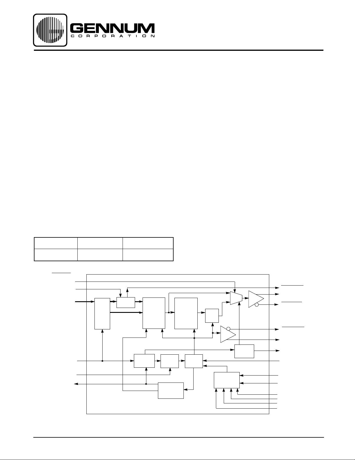
FUNCTIONAL BLOCK DIAGRAM
Revision Date: March 2001
GENNUM CORPORATION P.O. Box 489, Stn A, Burlington, Ontario, Canada L7R 3Y3 tel. (905) 632-2996 fax: (905) 632-5946
Gennum Japan Corporation C-101 Miyamae Village, 2-10-42 Miyamae, Suginami-ku, Tokyo 168-0081, Japan tel. (03) 3334-7700 fax (03) 3247-8839
Document No. 520 - 27 - 08
GS9002 - ENCODER DC ELECTRICAL CHARACTERISTICS
V
= 5V, VEE = 0V, T
CC
PARAMETER SYMBOL CONDITIONS MIN TYP MAX UNITS NOTES
Supply Voltage V
Power Consumption P
Supply Current I
TTL Inputs-HIGH V
TTL Inputs-LOW V
Logic Input Current I
TTL Outputs-HIGH V
TTL Outputs-LOW V
= 0°C to 70°C unless otherwise shown
A
S
D
S
IHmin
ILmax
INmax
OHminTA
OLmaxTA
Operating Range 4.75 5.0 5.25 V
SDO/SDO connected to (V
thru 100Ω resistors, PCK OUT
connected to VEE via 1kΩ
Same as above with SCK/SCK
also connected to (VCC-2V)
thru 100Ω resistors.
SDO/SDO connected to (V
thru 100Ω resistors, PCK OUT
connected to V
Same as above with SCK/SCK
to (V
CC
TA = 25°C 2.0 - - V
T
= 25°C - - 0.8 V
A
= 25°C 2.4 - - V
= 25°C - - 0.5 V
EE
-2V) V thru 100Ω resistors. - 170 205 mA see Figure 15
via 1kΩ
-2V)
CC
-2V) - 155 190 mA
CC
- 690 870 mW
- 710 900 mW
- 2.5 10 µA
Sync Detect O/P I
Serial Outputs High V
(SDO & SCK) Low V
OSYNC
OH
OL
TA=25°C, RL=100Ω to VCC-2V -0.875 - -0.7 V
(V
-2V) -1.8 - -1.5 V
CC
- - 4.0 mA SINK & SOURCE
with respect to V
GS9002 - ENCODER AC ELECTRICAL CHARACTERISTICS
V
= 5V, VEE = 0V, T
CC
PARAMETER SYMBOL CONDITIONS MIN TYP MAX UNITS NOTES
Serial Data Outputs bit rates BR
(SDO and SDO)
Serial Clock Outputs frequency ƒ
(SCK and SCK)
Serial Data to Clock Timing t
NOT RECOMMENDED
Lock Time t
Parallel Clock Output frequency ƒ
(PCK OUT)
Parallel Data & Clock Inputs
= 0°C to 70°C, V
A
signal swing V
rise/fall times tR, t
jitter t
signal swing V
LOOP FILTER
FOR NEW DESIGNS
signal swing V
rise/fall times tR, t
jitter t
risetime t
setup t
hold t
=2.6 V unless otherwise shown,
SDO
SDO
J(SDO)
SCK
SCK
D
LOCK
PCKO
PCKO
JPCKO
R
SU
HOLD
RL = 100Ω to 100 - 400 Mb/s
(V
-2 volts)
CC
TA = 25°C
F
143 Mb/s - 400 - ps p-p see Note 1
270 Mb/s - 300 - ps p-p see Fig. 16
RL = 100Ω to 100 - 400 MHz see Fig. 12, 13
(V
-2 volts)
CC
See Figure 9 - 1.4 - ns Data lags Clock
C
LOOP FILT
R
LOOP FILT
RL = 1kΩ to V
F
TA = 25°C 500 - - ps
= 0.1µF - 1 1.2 ms
= 3.9kΩ
EE
700 850 1000 mV p-p
- 500 - ps 20% - 80%
- 800 - mV p-p see Fig. 14
10 - 40 MHz ƒ
- 800 - mV p-p
- 700 - ps 20% - 80%
- 400 - ps p-p
3--ns
3--ns
PCKO
= ƒ
CC
SCK
/10
NOTE 1: Measured using PCK-IN as trigger source on 1GHz analog oscilloscope.
520 - 27 - 08
2
ABSOLUTE MAXIMUM RATINGS
PARAMETER VALUE/UNITS
Supply Voltage 5.5 V
Input Voltage Range (any input) -V
DC Input Current (any one input) 10 mA
Power Dissipation (V
Operating Temperature Range 0°C ≤ TA ≤ 70°C
Storage Temperature Range -65°C ≤ TS ≤150°C
Lead Temperature (soldering 10 seconds) 260°C
SYNC
DET.
DIS.
V
CC1VEE
SYNC
DET.
= 5.25 V) 1 W
S
V
CC3VEEVEE
SCK SCK
< VI < V
EE
CC
a
V
V
CC2
b
CC2
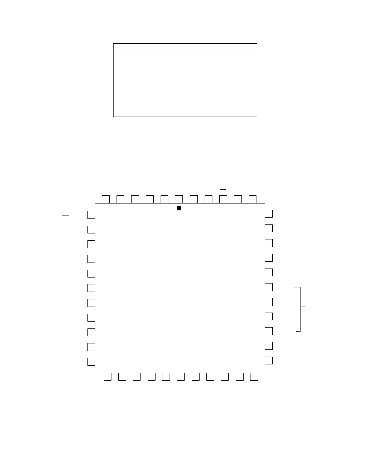
6 5 4 3 2 44 43 42 41 40
PD0
PD1
PD2
PARALLEL
DATA
INPUTS
NOT RECOMMENDED
PD3
PD4
PD5
PD6
PD7
PD8
PD9
7
8
9
10
11
12
13
14
15
16
GS9002
TOP VIEW
39
38
37
36
35
34
33
32
31
30
SDO
SDO
V
EE
DRS0
DRS1
RVC00
RVC01
RVC02
RVC03
V
EE
VCO
FREQUENCY
SET
RESISTORS
FOR NEW DESIGNS
PCK IN
17
18 19 20 21 22 23 24 25 26 27 28
29
C. REG
EE
OUT
DET.
LOCK
PCK
V
LOOP
V
CC3
FILT.
NC
V
EE
EE
SSSV
V
V
CC3
EE
Fig. 1 GS9002 Encoder Pin Connections
3
520 - 27 - 08
GS9002 Serial Digital Encoder - Detailed Device Description
The GS9002 Encoder is a bipolar integrated circuit used to
convert parallel data into a serial format according to the
SMPTE 259M standard. The device encodes both eight and
ten bit TTL-compatible parallel signals producing serial data
rates up to 400 Mb/s. It operates from a single five volt supply
and is packaged in a 44 pin PLCC.
Functional blocks within the device include the input latches,
sync detector, parallel to serial converter, scrambler, NRZ to
NRZI converter, ECL output buffers for data and clock, PLL for
10x parallel clock multiplication and lock detect.
The parallel data (PD0-PD9) and parallel clock (PCK-IN) are
applied via pins 7 through 17 respectively.
Sync Detector
The Sync Detector looks for the reserved words 000-003 and
3FC-3FF, in ten bit Hex, or 00 and FF in eight bit Hex, used in
the TRS-ID sync word. When the occurrence of either all zeros
or ones at inputs PD2-PD9 is detected, the lower two bits PD0
and PD1 are forced to zeros or ones, respectively. This makes
the system compatible with eight or ten bit data. For non SMPTE standard parallel data, a logic input, Sync Disable (6)
is available to disable this feature.
VCO Centre Frequency Selection
The wide VCO pull range allows the PLL to compensate for
variations in device processing, temperature variations and
changes in power supply voltage, without external adjustment.
A single external resistor is used to set the VCO current for
each of four centre frequencies as selected by a two bit code
through a 2:4 decoder.
The current setting resistors are connected to the RVCO0
through RVCO3 inputs (34, 33, 32 and 31). The decoder
inputs DRS0 and DRS1 (36, 35) are TTL compatible inputs
and select the four resistors according to the following truth
table.
DRS1 DRS0 Resistor Selected
0 0 RVCO0 (34)
0 1 RVCO1 (33)
1 0 RVCO2 (32)
1 1 RVCO3 (31)
Scrambler
The Scrambler is a linear feedback shift register used to
pseudo-randomize the incoming serial data according to the
fixed polynomial (X
in the output serial data stream. The NRZ to NRZI converter
uses another polynomial (X+1) to convert a long sequence of
ones to a series of transitions, minimizing polarity effects.
Phase Locked Loop
The PLL performs parallel clock multiplication and provides
the timing signal for the serializer. It is composed of
a phase/frequency detector, charge pump, VCO and a
divide-by-ten counter.
The phase/frequency detector allows a wider capture range
and faster lock time than that which can be achieved with a
phase discriminator alone. The discrimination of frequency
also eliminates harmonic locking. With this type of discriminator,
the PLL can be over-damped for good stability without
sacrificing lock time.
The charge pump delivers a 'charge packet' to the loop filter
which is proportional to the system phase error. Internal
voltage clamps are used to constrain the loop filter voltage
between approximately 1.8 and 3.4 volts.
NOT RECOMMENDED
9+X4
+1). This minimizes the DC component
FOR NEW DESIGNS
A 2:1 multiplexer (MUX) selects either the direct data from the
P/S Converter (Serializer) or the NRZI data from the Scrambler.
This MUX is controlled by the Scrambler/Serializer Select
(SSS) input pin 26. When this input is LOW the MUX selects
the Scrambler output. (This is the mode used for SMPTE
259M data). When this input is HIGH the MUX directly routes
the serialized data to the output buffer with no scrambling or
NRZ to NRZI
The lock detect circuit disables the serial data output when the
loop is not locked by turning off the 2:1 MUX. The Lock Detect
output is available from pin 20 and is HIGH when the loop is
locked.
The true and complement serial data, SDO and SDO are
available from pins 38 and 39 while the true and complement
serial clock, SCK and SCK are available from pins 43 and 42
respectively. If the serial clock is not used pins 43 and 42 can
be connected to V
The regenerated parallel clock (PCK OUT) is available at pin
19. This output is a single ended pseudo-ECL output requiring
a pull down resistor. If regenerated parallel clock is not used
pin 19 can be connected to V
conversion.
.
CC
CC
.
The VCO, constructed from a current-controlled multivibrator,
features operation in excess of 400 Mb/s and a wide pull range
(≈±40% of centre frequency).
520 - 27 - 08
4

GS9002 PIN DESCRIPTIONS
PIN NO. SYMBOL TYPE DESCRIPTION
1 V
2 V
3 SYNC DET. O TTL output level that detects the occurrence of all zero’s or all one’s at inputs PD2-PD9
4 V
5V
6 SYNC DET. I TTL level input that disables the internal Sync Detector when HIGH. This allows the
7-16 PD0-PD9 I TTL level inputs of the parallel data words. PD0 is the LSB and PD9 is the MSB.
17 PCK-IN I TTL level input of the Parallel Clock.
18 V
19 PCK OUT O Pseudo-ECL output representing the re-clocked Parallel Clock and is derived from the
20 LOCK DET. O TTL level output which goes HIGH when the internal PLL is locked.
21 V
22 LOOP FILT. I Connection for the R-C loop filter components. The loop filter sets the PLL loop
23 V
24 NC
EE
CC3
EE
CC1
DISABLE GS9002 to serialize 8 or 10 bit non - SMPTE Standard parallel data.
EE
CC3
EE
Power Supply: Most negative power supply connection.
Power Supply: Most positive power supply connection for the PLL and scrambler.
and pulses LOW for three PCK-IN durations. Used to detect SMPTE 259M reserved words
(000-003 and 3FC-3FF) in TRS sync word. Parallel data bits PD0 and PD1 are set Low or
High when PD2 - PD9 are Low or High respectively.
Power Supply: Most negative power supply connection.
Power Supply: Most positive power supply connection for the input data latches and serializer.
Power Supply: Most negative power supply connection.
internal VCO. The VCO is divided by 10 in order to produce this output.
Power Supply: Most positive power supply connection for the PLL and scrambler.
parameters.
Power Supply: Most negative power supply connection.
25 V
26 SSS I Scrambler/Serializer Select. TTL level input that selects scrambled NZRI output when
27 V
28 V
29 C
30 V
31 R
EE
EE
CC3
REG
EE
VCO3
I Compensation RC network for internal voltage regulator that requires decoupling with a series
I VCO Resistor 3: Analog current input used to set the centre frequency of the VCO when
NOT RECOMMENDED
32 R
VCO2
I VCO Resistor 2: Analog current input used to set the centre frequency of the VCO when
FOR NEW DESIGNS
33 R
34 R
35,36 DRS0, 1 I TTL level inputs to the internal 2:4 demultiplexer used to select one of four VCO frequency
VCO1
VCO0
I VCO Resistor 1: Analog current input used to set the centre frequency of the VCO when
I VCO Resistor 0: Analog current input used to set the centre frequency of the VCO when
Power Supply: Most negative power supply connection.
logic LOW or direct serializer output when logic HIGH.
Power Supply: Most negative power supply connection.
Power Supply: Most positive power supply connection for the PLL and scrambler.
0.1µF capacitor and 820Ω resistor. Components should be located as close as possible to the pin.
Power Supply: Most negative power supply connection.
the two Data Rate Select bits (pins 35 and 36) are both set to logic 1. A resistor is
connected from this pin to VEE.
the Data Rate Select Bit 0 (pin 36) is set to logic 0 and the Data Rate Select Bit 1 (pin 35)
is set to logic 1. A resistor is connected from this pin to VEE.
the Data Rate Select Bit 0 (pin 36) is set to logic 1 and the Data Rate Select Bit 1 (pin 35)
is set to logic 0. A resistor is connected from this pin to V
the two Data Rate Select bits (pins 35 and 36) are both set to logic 0. A resistor is
connected from this pin to VEE.
setting resistors (R
VCO0
- R
). (See above)
VCO3
EE
.
5
520 - 27 - 08

GS9002 PIN DESCRIPTIONS
PIN NO SYMBOL TYPE DESCRIPTION
37 V
38,39 SDO/SDO O Serial Data Outputs (true and inverse). Pseudo-ECL differential outputs representing the serialized
40 V
41 V
42,43 SCK/SCK O Serial Clock Outputs (inverse and true). Pseudo-ECL differential outputs of the Serial Clock (10x
44 V
INPUT / OUTPUT CIRCUITS
EE
CC2b
CC2a
EE
5k
Power Supply: Most negative power supply connection.
data. These outputs require 390Ω pull down resistors.
Power Supply: Most positive power supply connection for the Serial Data ECL output buffers.
Power Supply: Most positive power supply connection for the Serial Clock ECL output buffers.
Parallel Clock). These outputs require 390Ω pull-down resistors.
Power Supply: Most negative power supply connection.
V
V
CC
SYNC DET
INPUT
1k
1k
CC
V
R1
V
LOCK
DETECT
EE
V
EE
Fig. 2 Pin No. 3
Sync Detect
V
CC
NOT RECOMMENDED
1k
1k
FOR NEW DESIGNS
Fig. 4 Pin No. 19
Parallel Clock Out
V
CC
PCK OUT
V
EE
Fig. 3 Pins No. 6, 7 - 16, 17,26
Sync Disable, Parallel Data, Parallel Clock,
Scrambler/Serializer Select
V
CC
10k
V
EE
Fig. 5 Pin No. 20
Lock Detect
520 - 27 - 08
6

DRS0
I
VCO
V
R2
=2.15V
V
SELECT
V
CC
V
CC
DRS1
V
EE
Fig. 6 Pins No. 35, 36
Data Rate Select
200
200
800
R
VCOX
V
R1
V
EE
Fig. 7 Pins No. 31 - 34
Frequency Setting Registors R
V
CC
SERIAL OUT
(TRUE)
SERIAL OUT
(INVERT)
VCO0-RVCO3
PARALLEL
CLOCK
PLCK
PARALLEL
DATA
PDn
V
EE
Fig. 8 Pins No. 38, 39, 42, 43
NOT RECOMMENDED
t
CLKL = tCLKH
Serial Outputs (Data & Clock)
t
D
t
D
FOR NEW DESIGNS
SERIAL
DATA OUT
(SD0)
SERIAL
CLOCK OUT
(SCK)
Fig. 9 Waveforms
7
50%
50%
520 - 27 - 08
t
SU
50%
t
HOLD

4ƒ
sc
DATA
STREAM
SYNC
DETECT
T
ACTIVE VIDEO
R
& H BLANKING
S
T
ACTIVE VIDEO
R
& H BLANKING
S
T
R
S
4:2:2
DATA
STREAM
SYNC
DETECT
PCLK IN
PDN
SYNC
DETECT
E
H
S
A
BLNK
V
XXX 3FF 000 000 XXX ••• ••• XXX 3FF 000 000 XXX •••
ACTIVE
A
VIDEO
V
E
H
BLNK
S
A
V
A
V
Fig. 10 Timing Diagram
+5V
LOOP
LOCKED
L.E.D.
330
+5V
DATA 0
DATA 1
DATA 2
DATA 3
DATA 4
DATA 5
DATA 6
DATA 7
DATA 8
DATA 9
CLOCK
*150
NOT RECOMMENDED
DATA RATE
SELECT DIP
SWITCH
(SEE TRUTH TABLE,
FIG. 2)
FOR NEW DESIGNS
10k
*10p
+5V
10k
2N4400
0.1
820
10k
7
8
9
10
11
12
13
14
15
16
17
36
35
29
5k
20 26 6 2,5,21,28,40,41
LOCK SSS SYNC (6x VCC)
PD0
DET. DIS.
PDI
PD2
PD3
PD4
PD5
PD6
PD7
PD8
PD9
PCK IN
DRS0
DRS1
CREG
RVCO1 RVCO2 RVCO3 RVCO4 VEE
4x0.1
GS9002
34 33 32 31 1,4
1 2 3 4
+10
6x100n
SDO
SDO
SCK
SCK
PCK-OUT
LOOP FILT
18,23
25,27
30,37
44
0.1
82
100
1k
100
COMMON
DATA
DATA
CLOCK
CLOCK
PARALLEL
CLOCK OUT
100
100
38
39
43
42
+5V
19
22
1M
0.1
3.9k
NOTES: Resistors 1, 2, 3 and 4 are used to set the VCO centre frequency. For 143/177 Mb/s
All resistors in ohms, all capacitors in microfarads unless otherwise stated. represent test points.
* This RC network is used to slow down fast PCLK risetimes ( ≤ 500ps). It is not required if risetimes exceed 500ps.
Fig. 11 GS9002 Test Circuit
520 - 27 - 08
8
≈ 6kΩ, 270 Mb/s ≈ 2.7kΩ, 360 Mb/s ≈ 1.8kΩ

TYPICAL PERFORMANCE CURVES (VS = 5V, TA = 25° C unless otherwise shown)
600
550
500
450
400
350
300
250
200
VCO FREQUENCY (MHz)
150
100
50
V
LOOP
0 1 2 3 4 5 6 7 8 9 10
FREQUENCY SETTING RESISTANCE (kΩ)
Fig. 12 VCO Frequency
1000
950
900
850
VS= 5.25V
VS= 5.0V
=2.6V
600
550
500
450
400
350
300
250
200
FREQUENCY (MHz)
150
100
50
0
1.8 2.0 2.2 2.4 2.6 2.8 3.0 3.2 3.4
OPTIMAL
LOOP FILTER
VOLTAGE
LOOP FILTER VOLTAGE (V)
R
= 1.8k
VCO
Fig. 13 VCO Frequency vs Loop Filter Voltage
200
V
S
190
180
V
R
VCO
R
VCO
= 5.25V
= 5.0V
S
= 2.7k
= 6.3k
800
SERIAL OUTPUT (mV)
750
700
0 10 20 30 40 50 60 70
AMBIENT TEMPERATURE (°C)
VS= 4.75V
Fig. 14 Serial Output Level (Data & Clock)
NOT RECOMMENDED
800
700
600
500
400
300
JITTER p-p (ps)
200
100
1.8 2.0 2.2 2.4 2.6 2.8 3.0 3.2 3.4
FOR NEW DESIGNS
143 Mb/s
270 Mb/s
LOOP FILTER VOLTAGE (V)
170
CURRENT (mA)
160
150
0 10 20 30 40 50 60 70
AMBIENT TEMPERATURE (°C)
VS= 4.75V
Fig. 15 Supply Current
Fig. 16 Output Jitter
9
520 - 27 - 08

+5V
SDO1
(75Ω)
SDO1
(75Ω)
1p8
SDO2
(75Ω)
SDO2
(75Ω)
SERIAL
CLOCK
(50Ω)
5
4x150
+5V
1p8
68
PARALLEL CLOCK T.P.
1M
This signal is 12dB
below actual SCK
level and is used for
test purposes
DATA RATE SELECT
0 0 0
0 1 1
0.1
27
47
DRS1 DRS0 RVCO NO.
18p
47
100
0.1
1 0 2
180
1 1 3
TRUTH TABLE
rail.
EE
Serial Digital Chipset
™
1.0
3
OUT 2
SER . IN
6
100
68
1.0
4
OUT 2
VEE
390
1p8
1p8
68
10
+
0.1µ
68
1.0
1.0
1
2
OUT 1
OUT 1
8
VCC
CABLE
DRIVER
GS9007
SER. IN
7
100
1k
3.9k
38
10
+
6x100n
SDO
390
39
SDO
43
SCK
42
19
22
SCK
PCK-OUT
GS9002
5k
20 26 6 2,5,21,28,40,41
LOCK SSS SYNC (6x VCC)
+5V
7
100
*
DET. DIS.
PD0
PDI
PD2
PD3
9
10111213141516
100
100
DATA 1
DATA 2
DATA 3
100
DATA 0
8
PD4
100
DATA 4
PD5
100
DATA 5
PD6
100
DATA 6
PD7
100
DATA 7
PD8
100
DATA 8
PD9
100
DATA 9
100
PCK IN
DRS0
173635
10pF
CLOCK
DRS1
NOT RECOMMENDED
10k
FOR NEW DESIGNS
2N4400
330
LOOP
LOCKED
L.E.D.
0.1
18,23
25,27
30,37
44
LOOP FILT
1 2 3 4
34 33 32 31 1,4
RVCO0 RVCO1 RVCO2 RVCO3 VEE
CREG
29
0.1
10k
10k
820
4x0.1
+5V
GENLINX
GS9002/7 Application Circuit
Fig. 17
520 - 27 - 08
10
DATA RATE
SELECT DIP
SWITCH
(SEE TRUTH TABLE)
These resistors are used to slow down fast INPUT edges ( ≤500ps ) and prevent the input signals from ringing below the V
*
NOTES: Resistors 1, 2, 3 and 4 are used to set the VCO centre frequency. See Figures 12 and 13.
All resistors in ohms, all capacitors in microfarads unless otherwise stated. represent test points.

APPLICATION CIRCUIT
Figure 17 shows a typical application circuit of the GS9002
driving a GS9007 cable driver.
An applications board is fully described in Application Note
520-83, entitled 'Serial Digital Encoder Board Using the
GS9002 and GS9009'. The board and application note are
available from Gennum Corporation.
NOT RECOMMENDED
DOCUMENT
IDENTIFICATION
FOR NEW DESIGNS
REVISION NOTES
Watermark added.
For latest product information, visit www.gennum.com
CAUTION
ELECTROSTATIC
SENSITIVE DEVICES
DO NOT OPEN PACKAGES OR HANDLE
EXCEPT AT A STATIC-FREE WORKSTATION
Gennum Corporation assumes no responsibility for the use of any circuits described herein and makes no representations that they are free from patent infringement.
© Copyright March 1991 Gennum Corporation. All rights reserved. Printed in Canada.
11
PRODUCT PROPOSAL
This data has been compiled for market investigation purposes
only, and does not constitute an offer for sale.
ADVANCE INFORMATION NOTE
This product is in development phase and specifications are
subject to change without notice. Gennum reserves the right to
remove the product at any time. Listing the product does not
constitute an offer for sale.
PRELIMINARY
The product is in a preproduction phase and specifications are
subject to change without notice.
DATA SHEET
The product is in production. Gennum reserves the right to
make changes at any time to improve reliability, function or
design, in order to provide the best product possible.
520 - 27 - 08
 Loading...