

Page 1

GS4915 ClockCleaner™
GS4915 Data Sheet
Key Features
• Reduces jitter for clocks of 148.5MHz,
148.5/1.001MHz, 74.25MHz, 74.25/1.001MHz and
27MHz
• Output jitter as low as 20ps peak to peak
• Automatic bypass mode for all other clock rates
• Loop bandwidth adjustable as low as 2kHz
• Output skew control
• Input selectable as differential or single-ended
• Both single-ended and differential outputs
• Uses the GO1555 VCO
• Small 6mm x 6mm 40-pin QFN package
• Pb-free and RoHS compliant
Applications
High definition video systems. Digital video recording,
playback, processing and display devices.
Description
The GS4915 provides a low jitter clock output when fed
with an HD or SD video clock input. Other input clock
frequencies between 12MHz and 165MHz can be
automatically passed through to the GS4915 outputs.
An internal 2:1 mux allows the user to select between a
differential or single-ended (LVCMOS) input clock. Both
a single-ended LVCMOS- compatible and an
LVDS-compatible differential output are provided.
The GS4915 may operate in either auto or fixed
frequency mode. In auto mode, the device will
automatically clean the selected input clock if its
frequency is found to be one of the supported SD or HD
clock rates. In fixed mode, the user selects only one of
these frequencies to be cleaned.
In addition, the device allows the user to select between
auto or manual bypass operation. In autobypass mode,
the GS4915 will automatically bypass its cleaning stage
and pass the input clock signal directly to the output
whenever the device is unlocked, which includes the
case where the input frequency is something other than
the five frequencies supported. In manual bypass
mode, the input signal passes through directly to the
output.
The GS4915 can optionally double the output frequency
for 74.25MHz or 74.175MHz HD clocks in order to
provide optimal jitter performance of some serializers.
The GS4915 also provides the user with a 2-state skew
control. The output clocks produced by the device may
be advanced by ¼ of an output CLK period in order to
accommodate downstream setup and hold
requirements.
The GS4915 is designed to operate with the GO1555
VCO.
The GS4915 Clock Cleaner complements Gennum's
GS4911B Clock and Timing Generator for
implementing a video genlock solution. Whereas the
GS4911B itself cleans low-frequency jitter, the GS4915
is designed to clean primarily the higher frequency jitter
of clocks generated by the GS4911B.
39145 - 4 February 2008 1 of 26
www.gennum.com
Page 2
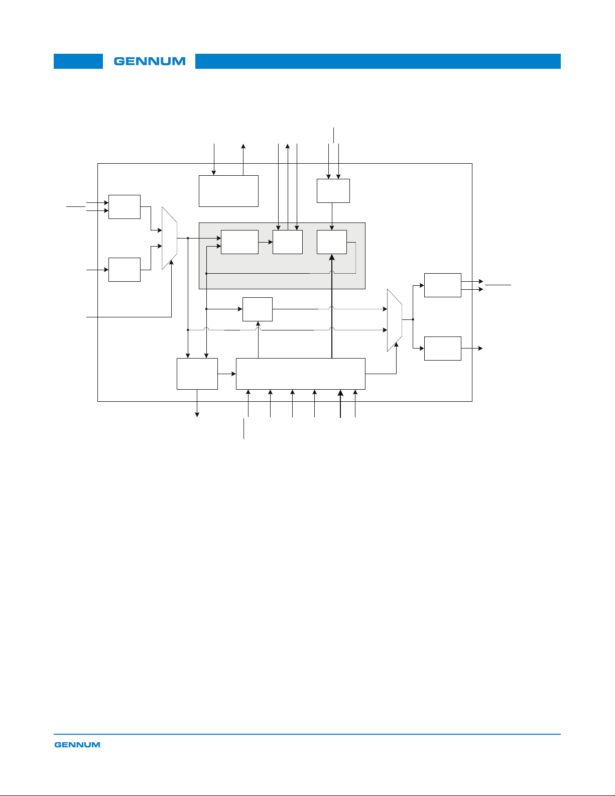
Functional Block Diagram
2.5V Regulator
Phase
Detector
Charge
Pump
Divide
by N
Skew
Select
Digital Control Block
Frequency
Detection
DIFF I/P
Buffer
S-E I/P
Buffer
Clock Cleaning PLL
DIFF O/P
Buffer
S-E O/P
Buffer
CLKIN
CLKIN
CLKIN_SE
IPSEL
CLKOUT_SE
CLKOUT
CLKOUT
SKEW_EN
BYPASS
AUTOBYPASS
FCTRL[1:0]
DOUBLE
REG_VDD
VCO_VDD
CP_VDD
LF
VCO
Receiver
VCO
CP_RES
LOCK
clkout
clkin
bypass
RESET
VCO
0
1
0
1
GS4915 Data Sheet
39145 - 4 February 2008 2 of 26
GS4915 Functional Block Diagram
Page 3
GS4915 Data Sheet
Contents
Key Features.................................................................................................................1
Applications...................................................................................................................1
Description ....................................................................................................................1
Functional Block Diagram .............................................................................................2
1. Pin Out ......................................................................................................................4
1.1 Pin Assignment ...............................................................................................4
1.2 Pin Descriptions ..............................................................................................5
2. Electrical Characteristics...........................................................................................8
2.1 Absolute Maximum Ratings ............................................................................8
2.2 DC Electrical Characteristics ..........................................................................8
2.3 AC Electrical Characteristics .........................................................................10
2.4 Solder Reflow Profiles ...................................................................................11
3. Detailed Description ................................................................................................12
3.1 Functional Overview .....................................................................................12
3.2 Clock Inputs ..................................................................................................12
3.2.1 Differential Clock Input.........................................................................13
3.2.2 Single-Ended Clock Input ....................................................................13
3.2.3 Input Clock Selection ...........................................................................13
3.2.4 Unused Clock Inputs............................................................................13
3.3 Clock Cleaning PLL ......................................................................................13
3.3.1 Phase Detector ....................................................................................14
3.3.2 Charge Pump.......................................................................................14
3.3.3 Loop Filter............................................................................................14
3.3.4 External VCO.......................................................................................15
3.4 Modes of Operation ......................................................................................15
3.4.1 Frequency Modes ................................................................................15
3.4.2 Bypass Modes .....................................................................................17
3.5 Output Clock Frequency and Jitter ...............................................................18
3.6 Output Skew .................................................................................................20
3.7 Clock Outputs ...............................................................................................21
3.7.1 Differential Clock Output......................................................................21
3.7.2 Single-Ended Clock Output .................................................................21
3.8 Device Reset .................................................................................................21
3.8.1 Hardware Reset...................................................................................21
4. Typical Application Circuit .......................................................................................22
5. References & Relevant Standards..........................................................................23
6. Package & Ordering Information.............................................................................24
6.1 Package Dimensions ....................................................................................24
6.2 Recommended PCB Footprint ......................................................................25
6.3 Packaging Data .............................................................................................25
6.4 Ordering Information .....................................................................................25
7. Revision History ......................................................................................................26
39145 - 4 February 2008 3 of 26
Page 4
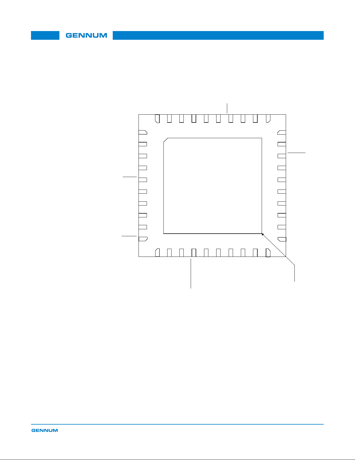
1. Pin Out
AGND
VCO_ VDD
CP_ VDD
CP_ RES
LF
VCO_ GND
VCO
VCO
DIV_VDD
AGND
REG_VDD
AGND
PD_VDD
CLKIN
CLKIN
AGND
IN_VDD
CLKIN_SE
AGND
RESET
GS4915
40-pin QFN
(Top View )
AGND
CLKOUT
DIFF_OUT_VDD
AGND
D_VDD
CLKOUT_SE
SE_ VDD
GND
LOCK
IPSEL
GND
BYPASS
AUTOBYPASS
D_ V DD
FCTRL0
FCTRL1
DOUBLE
SKEW_EN
GND
1
2
3
4
5
6
7
8
9
10 21
22
23
24
25
26
27
28
29
30
31323334353637383940
11 12 13 14 15 16 17 18 19 20
Ground Pad
(Bottom of Package)
CLKOUT
1.1 Pin Assignment
GS4915 Data Sheet
Figure 1-1: 40-Pin QFN
39145 - 4 February 2008 4 of 26
Page 5
1.2 Pin Descriptions
Table 1-1: Pin Descriptions
GS4915 Data Sheet
Pin
Name Timing Type Description
Number
1 REG_VDD – Power Positive power supply connection for the internal voltage regulator.
Connect to filtered +3.3V DC.
2, 6, 9, 26,
30, 31, 40
3 PD_VDD – Power Positive power supply connection for the phase detector. Connect to
4, 5 CLKIN, CLKIN
7 IN_VDD – Power Positive power supply connection for the single-ended and differential
8 CLKIN_SE – Input CLOCK SIGNAL INPUT
10 RESET
11 IPSEL Non
AGND – Power Ground connection for analog blocks and IO’s. Connect to clean analog
– Input CLOCK SIGNAL INPUTS
Non
synchronous
synchronous
Input CONTROL SIGNAL INPUT
Input CONTROL SIGNAL INPUT
GND.
filtered +1.8V DC.
Signal levels are CML/LVDS compatible.
A differential clock input signal is applied to these pins.
input clock buffers. Supplies CLKIN_SE. Connect to filtered +1.8V DC.
Signal levels are LVCMOS compatible.
A single-ended video clock input signal is applied to this pin.
Signal levels are LVCMOS/LVTTL compatible.
See Section 3.8.1 for operation.
Signal levels are LVCMOS compatible.
Selects which input clock is cleaned by the device.
See Section 3.2.3 for operation.
12, 20, 22 GND – Power Ground connection for digital blocks and IO’s. Connect to GND.
13 BYPASS Non
synchronous
14 AUTOBYPASS
15 D_VDD – Power Positive power supply connection for digital block. Connect to filtered
17, 16 FCTRL1, FCTRL0 Non
Non
synchronous
synchronous
39145 - 4 February 2008 5 of 26
Input CONTROL SIGNAL INPUT
Signal levels are LVCMOS compatible.
See Manual Bypass Section 3.4.2.
Input CONTROL SIGNAL INPUT
Signal levels are LVCMOS compatible.
Selects the bypass mode of the device.
See Manual Bypass Section 3.4.2.
+1.8V DC. The digital block includes pins 10 - 21.
Input CONTROL SIGNAL INPUTS
Signal levels are LVCMOS compatible.
Selects the frequency mode of the device.
See Section 3.4.1 for operation.
Page 6
Table 1-1: Pin Descriptions (Continued)
GS4915 Data Sheet
Pin
Name Timing Type Description
Number
18 DOUBLE Non
synchronous
19 SKEW_EN Non
synchronous
21 LOCK Non
synchronous
23 SE_VDD – Power Positive power supply connection for the single-ended clock driver.
24 CLKOUT_SE – Output CLOCK SIGNAL OUTPUT
Input CONTROL SIGNAL INPUT
Signal levels are LVCMOS compatible.
Controls the output frequency of the cleaned clock, for HD input clocks.
See Section 3.5 for operation.
Input CONTROL SIGNAL INPUT
Signal levels are LVCMOS compatible.
Selects the phase of the output clock with respect to the selected input
clock.
See Section 3.6 for operation.
Output STATUS SIGNAL OUTPUT
Signal levels are LVCMOS compatible.
This pin will be HIGH when the output clock is locked to the selected input
clock.
It will be LOW otherwise.
Determines the output level of CLKOUT_SE. Connect to filtered +1.8V DC
or +3.3V DC.
NOTE: If the single-ended clock output is not used, this pin should be tied
to ground.
Signal levels are LVCMOS compatible.
Single-ended video clock output signal.
See Section 3.7.2 for operation.
25 D_VDD – Power Positive power supply connection for the single-ended output clock buffer.
27 DIFF_OUT_VDD – Power Positive power supply connection for the LVDS clock outputs. Connect to
29, 28 CLKOUT,
CLKOUT
32 DIV_VDD – Power Positive power supply connection for the divider block. Connect to filtered
33,34 VCO, VCO
35 VCO_GND – Power Ground reference for the external voltage controlled oscillator. Connect to
– Output CLOCK SIGNAL OUTPUT
Analog Input Differential input for the external VCO reference signal. When using the
39145 - 4 February 2008 6 of 26
Connect to filtered +1.8V DC.
NOTE: If the single-ended clock output is not used, this pin should be tied
to ground.
filtered +1.8V DC.
NOTE: If the LVDS clock outputs are not used, this pin should be tied to
ground.
Differential video clock output signal.
This is the lowest jitter output of the device.
See Section 3.7.1 for operation.
+1.8V DC.
recommended VCO, leave VCO
See Section 3.3.4 for operation.
pins 2, 4, 6, and 8 of the GO1555.
unconnected.
Page 7
Table 1-1: Pin Descriptions (Continued)
GS4915 Data Sheet
Pin
Name Timing Type Description
Number
36 LF Analog Output Control voltage for the external voltage controlled oscillator. Connect to pin
5 of the GO1555 via a low pass filter. See Typical Application Circuit on
page 22.
37 CP_RES Analog Input Charge pump current control.
Connect to VCO_GND via a 10kΩ resistor.
38 CP_VDD – Power Power supply for the internal charge pump block (nominally +2.5V DC).
Connect to VCO_VDD (pin 39).
39 VCO_VDD – Power Power supply for the external voltage controlled oscillator (+2.5V DC).
Connect to pin 7 of the GO1555. This pin is an output.
Must be isolated from all other power supplies.
– Ground Pad – Power Ground pad on bottom of package must be soldered to AGND plane of
PCB.
39145 - 4 February 2008 7 of 26
Page 8
2. Electrical Characteristics
2.1 Absolute Maximum Ratings
Parameter Value
GS4915 Data Sheet
Supply Voltage (SE_VDD, REG_VDD) -0.3 to +4.0 V
Core Supply Voltage (all 1.8V supplies) -0.3 to +2.2 V
Input ESD Voltage 1 kV HBM
Storage Temperature -50ºC < T
Operating Temperature -20ºC < T
NOTE: Absolute Maximum Ratings are those values beyond which damage to the device may
occur. Functional operation under these conditions or at any other condition beyond those
indicated in the AC/DC Electrical Characteristic sections is not implied.
DC
DC
< 125ºC
S
< 85ºC
A
2.2 DC Electrical Characteristics
Table 2-1: DC Electrical Characteristics
VDD = 1.8V ±5%, 3.3V ±5%; TA = -20ºC to 85ºC, unless otherwise shown
Parameter Symbol Conditions Min Typ Max Units Notes
Operating Temperature Range T
Power Consumption
(SE_VDD = 1.8V Nominal)
A
P
1.8V
– -20 25 85 ºC –
1.8V Rail – 156 270 mW –
3.3V Rail – 58 87 mW –
Power Consumption
(SE_VDD = 3.3V Nominal)
+1.8V Power Supply Voltage – – 1.71 1.8 1.89 V –
+3.3V Power Supply Voltage – – 3.135 3.3 3.465 V –
+2.5V Regulator Output Voltage – Output load of 3-12mA 2.375 2.5 2.625 V –
Input Voltage, Logic LOW V
Input Voltage, Logic HIGH V
Output Voltage, Logic LOW V
Output Voltage, Logic HIGH V
P
3.3V
IL
IH
OL
OH
39145 - 4 February 2008 8 of 26
1.8V Rail – 132 243 mW –
3.3V Rail – 133 156 mW –
– – 0 0.35 x
IO_VDD
– 0.65 x
IO_VDD
1.8V or 3.3V operation – 0 0.4 V 2,3,5
1.8V operation 0.65 x
IO_VDD
3.3V operation 0.65 x
IO_VDD
1.8 – V 1,5
1.8 – V 2,3,5
3.3 – V 2,3,5
V1,5
Page 9

GS4915 Data Sheet
VOCM
0V
CLKOUT
CLKOUT
CLKOUT - CLKOUT
VODIFF
+VODIFF
-VODIFF
Table 2-1: DC Electrical Characteristics (Continued)
VDD = 1.8V ±5%, 3.3V ±5%; TA = -20ºC to 85ºC, unless otherwise shown
Parameter Symbol Conditions Min Typ Max Units Notes
Clock Output Drive Current – 1.8V operation – 10 – mA 2,3,4
3.3V operation – 8 – mA 2,3,4
Differential Input Common Mode
Voltage
Differential Input Swing V
Differential Clock Output Common
Mode Voltage
V
V
ICM
IDIFF
OCM
– 1.121.251.38 V –
– 240 350 460 mV –
100Ω termination
–1.45– V –
between CLKOUT and
CLKOUT
Differential Clock Output Swing V
ODIFF
100Ω termination
between CLKOUT and
250 350 460 mV 6
CLKOUT
NOTES:
1. For all LVCMOS compatible inputs.
2. For LVCMOS compatible output SE_CLK.
3. For LVCMOS compatible output LOCK.
4. While still satisfying V
max and VOH min.
OL
5. IO_VDD refers to the power supply that supplies the particular pin in question. D_VDD supplies pins 10-21. IN_VDD supplies CLKIN_SE.
SE_VDD supplies CLKOUT_SE.
6. Differential swing as defined here:
39145 - 4 February 2008 9 of 26
Page 10

GS4915 Data Sheet
2.3 AC Electrical Characteristics
Table 2-2: AC Electrical Characteristics
VDD = 1.8V ±5%, TA = 0ºC to 70ºC, unless otherwise shown
Parameter Symbol Conditions Min Typ Max Units Notes
Input Jitter Tolerance IJT < 0.5Hz -10 – 10 UI 1
0.5Hz to 1Hz -5 – 5 UI 1
1Hz to 100Hz -1 – 1 UI 1
> 100Hz -0.1 – 0.1 UI 1
Output Jitter
Differential Output
Output Jitter
Single-ended Output
Output Duty Cycle – Differential output 45 – 55 % –
Differential Clock Output Rise / Fall Time – 100Ω diff. load – 500 – ps –
Single-ended Clock Output Rise / Fall Time – 10 pF load – 1200 – ps –
Input Clock Frequency – – 12 – 165 MHz –
Output Clock Frequency – – 12 – 165 MHz –
Lock Detect Time t
Unlock Detect Time t
Lock Time t
Device Latency – Differential in,
– 100kHz to 10MHz – 20 – ps –
– Unfiltered – 40 – ps –
– 100kHz to 10MHz – 60 – ps –
– Unfiltered – 100 – ps –
Single-ended output 40 – 60 % –
LOCKD
UNLOCKD
LOCK
Within 300ppm of
reference frequency
Within 700ppm of
reference frequency
– ––1s2
Differential out,
SKEW_EN = LOW
– – 500 us –
– – 500 us –
–1.2–ns–
Differential in,
Differential out,
SKEW_EN = HIGH
Single ended in,
single ended out,
SKEW_EN = LOW
Single ended in,
single ended out,
SKEW_EN = HIGH
Device Latency Difference – – – 750 – ps 3
NOTES:
1. One UI refers to one cycle of the input CLK.
2. Assuming power up has already occured.
3. Difference between cleaning and bypass modes.
39145 - 4 February 2008 10 of 26
– 1.2 -
T
/4
out
–3.5–ns–
– 3.5 -
T
/4
out
–ns–
–ns–
Page 11

2.4 Solder Reflow Profiles
25˚C
100˚C
150˚C
183˚C
230˚C
220˚C
Time
Temperature
6 min. max
120 sec. max
60-150 sec.
10-20 sec.
3˚C/sec max
6˚C/sec max
25˚C
150˚C
200˚C
217˚C
260˚C
250˚C
Time
Temperature
8 min. max
60-180 sec. max
60-150 sec.
20-40 sec.
3˚C/sec max
6˚C/sec max
The device is manufactured with Matte-Sn terminations and is compatible with both
standard eutectic and Pb-free solder reflow profiles. The recommended standard
eutectic reflow profile is shown in Figure 2-1. MSL qualification was performed
using the maximum Pb-free reflow profile shown in Figure 2-2.
GS4915 Data Sheet
Figure 2-1: Standard Eutectic Solder Reflow Profile
Figure 2-2: Maximum Pb-Free Solder Reflow Profile (Preferred)
39145 - 4 February 2008 11 of 26
Page 12

3. Detailed Description
3.1 Functional Overview
The GS4915 provides a low jitter clock output when fed with an HD or SD video
clock input. Other input clock frequencies between 12MHz and 165MHz can be
automatically passed through to the GS4915 outputs.
An internal 2:1 mux allows the user to select between a differential (CML/LVDS
compatible) or single-ended (LVCMOS) input clock. Both a single-ended
LVCMOS-compatible and an LVDS-compatible differential output are provided.
The GS4915 may operate in either auto or fixed frequency mode. In auto mode,
the device will automatically clean the selected input clock if its frequency is found
to be one of the supported SD or HD clock rates. In fixed mode, the user selects
only one of these frequencies to be cleaned.
In addition, the device allows the user to select between auto or manual bypass
operation. In autobypass mode, the GS4915 will automatically bypass its cleaning
stage and pass the input clock signal directly to the output whenever the device is
unlocked which includes the case where the input frequency is something other
than the five frequencies supported. In manual bypass mode, the input signal
passes through directly to the output.
GS4915 Data Sheet
3.2 Clock Inputs
The GS4915 can optionally double the output frequency for 74.25MHz or
74.175MHz HD clocks in order to provide optimal jitter performance of some
serializers.
The GS4915 also provides the user with a 2-state skew control. The output clocks
produced by the device may be advanced by ¼ of an output CLK period in order
to accommodate downstream setup and hold requirements.
The GS4915 is designed to operate with the GO1555 VCO.
The GS4915 Clock Cleaner complements Gennum's GS4911B Clock and Timing
Generator for implementing a video genlock solution. Whereas the GS4911B itself
cleans low-frequency jitter, the GS4915 is designed to clean primarily the higher
frequency jitter of clocks generated by the GS4911B.
The GS4915 contains two separate input buffers to accept either a differential or
single-ended input clock. The applied clock(s) can be any video clock needing
cleaning, although typically it will be the video clock specifically used for
serialization.
The frequency of the applied clock signal(s) must be between 12MHz and 165MHz.
The clock input buffers use a separate power supply of +1.8V DC supplied via the
IN_VDD pin.
39145 - 4 February 2008 12 of 26
Page 13

3.2.1 Differential Clock Input
A differential LVDS clock signal conforming to the TIA/EIA-644-A standard may be
AC-coupled to the CLKIN and CLKIN
GS4915 Data Sheet
pins.
If the GS4911B/10B/01B/00B is used, the PCLK3 and PCLK3
device may be directly connected to the CLKIN and CLKIN
respectively.
The CLKIN and CLKIN
differential impedance of 100Ω. The pair should be terminated with 100Ω at the
input to the device as no internal termination is provided.
This input clock is selected as the one to be cleaned by the GS4915 when the
IPSEL pin is set LOW.
The clock can be DC coupled if the levels are appropriate, but only AC coupling is
recommended. These inputs are both LVDS and CML compatible, and AC
coupling is only required in cases where the common mode does not line up.
3.2.2 Single-Ended Clock Input
A single-ended clock signal at from 1.8V - 3.3V CMOS levels may be DC-coupled
to the CLKIN_SE pin.
If the GS4911B/10B/01B/00B is used, the PCLK1 or PCLK2 output from that
device may be directly connected to the CLKIN_SE input of the GS4915.
3.2.3 Input Clock Selection
outputs from that
inputs of the GS4915,
input traces should be tightly-coupled with a controlled
An internal 2x1 input multiplexer is provided to allow switching between the
differential and single-ended clock inputs using one external pin. When IPSEL is
set LOW, the differential clock at the CLKIN/CLKIN
be processed by the device. When IPSEL is set HIGH, the single-ended clock at
the CLKIN_SE pin is selected as the one to be processed.
3.2.4 Unused Clock Inputs
If the application will only provide a differential clock input, then the CLKIN_SE
input pin should be connected to AGND.
If only a single-ended clock will be provided, then the CLKIN/CLKIN
left unconnected.
3.3 Clock Cleaning PLL
To obtain a low-jitter output clock signal, the GS4915 uses a clock cleaning
phase-locked loop. This block will always attempt to lock an external 1.485GHz
VCO signal to the selected input clock. Internal dividers, set by the digital control
block based on the frequency mode of the device (see Section 3.4.1), are used to
obtain the final output clock of 27MHz (divide by 55), 74.25MHz/74.175MHz (divide
by 20), or 148.5MHz/148.35MHz (divide by 10).
pins is selected as the one to
pins should be
39145 - 4 February 2008 13 of 26
Page 14

3.3.1 Phase Detector
3.3.2 Charge Pump
3.3.3 Loop Filter
GS4915 Data Sheet
The GS4915's phase detector can identify phase misalignment between the
selected input clock and the reference clock provided by the external VCO, and
correspondingly signal the charge pump to alter the VCO control voltage.
The charge pump block of the PLL is powered externally by +2.5V DC applied to
CP_VDD. This is provided by the GS4915 itself at the VCO_VDD pin. An external
RC filter at the CP_VDD pin is recommended to reduce supply noise for best jitter
performance. Please refer to the Typical Application Circuit on page 22.
An external resistance connected to the CP_RES pin is used to set the charge
pump reference current of the device. Typically, the CP_RES pin will be connected
through 10kΩ to VCO_GND.
The GS4915 PLL loop filter is an external first order filter formed by a series RC
connection as shown in Table 3-1: Loop Filter Component Values. The loop filter
resistor value sets the bandwidth of the PLL and the capacitor value controls its
stability and lock time. A loop filter resistor value between 1 Ω and 20 Ω and a loop
filter capacitor value between 1µF and 33µF are recommended.
The GS4915 uses a non-linear, bang-bang, PLL, therefore its bandwidth scales
linearly with the input jitter amplitude - greater input jitter results in a smaller loop
bandwidth causing more of the input jitter to be rejected. For a given input jitter
amplitude, a smaller loop filter resistor produces a narrower loop bandwidth. With
an input jitter amplitude of 300ps, for example, the PLL bandwidth can be adjusted
from 2KHz to 40KHz by varying the loop filter resistor, as shown in the table below.
For use with GS4911, a narrow loop bandwidth is recommended.
Increasing the loop filter capacitor value increases the stability of the PLL, but
results in a longer lock time. For loop filter resistors smaller than 7Ω, a capacitor
value of 33µF is recommended, while larger resistor values can accommodate
smaller capacitors. Sample combinations of the loop filter resistor and capacitor
values are shown in the table below, along with the resulting loop bandwidth.
Additional loop bandwidths can be achieved by using different loop filter resistor
values.
Table 3-1: Loop Filter Component Values
Loop Filter RTypical Loop
Bandwidth*
1Ω 2kHz 33μF Narrow bandwidth - provides maximum jitter reduction. Long lock-time.
7Ω 8kHz 10μF
Recommended
Loop Filter C
Comments
20Ω 40kHz 1μF Wide bandwidth. Fast lock-time.
Note:
1. *Measured with 300ps pk-pk input jitter on CLK.
39145 - 4 February 2008 14 of 26
Page 15

3.3.4 External VCO
The GS4915 uses the external GO1555 Voltage Controlled Oscillator as part of its
phase-locked loop. This external VCO implementation was chosen to ensure
superior jitter performance of the device.
Power for the external VCO is generated entirely by the GS4915 from an on-chip
voltage regulator. The internal regulator uses +3.3V DC supplied at the REG_VDD
pin to provide +2.5V at the VCO_VDD pin.
Based on the control voltage output by the GS4915 on the LF pin, the GO1555
produces a 1.485GHz reference signal for the PLL. This signal must be run via a
50Ω controlled-impedance trace to the VCO pin of the GS4915. The VCO receiver
block of the device will then convert this single-ended signal into the differential
1.485GHz reference signal used by the clock cleaning PLL.
Both the reference and controls signals should be referenced to the supplied
VCO_GND, as shown in the recommended application circuit of the Typical
Application Circuit on page 22.
3.4 Modes of Operation
GS4915 Data Sheet
3.4.1 Frequency Modes
The GS4915 may operate in one of two possible frequency modes, and in one of
three possible bypass modes. The combination of the frequency mode and bypass
mode will determine the frequency and jitter of the output clock.
The frequency mode of the device is determined entirely by the setting of the
external FCTRL[1:0] pins.
Table 3-2: GS4915 Frequency Modes
FCTRL[1:0] Frequency Mode
00 Auto
01 Fixed – 27MHz ± 0.4%
10 Fixed – 74.25MHz ± 0.4%
11 Fixed – 148.5MHz ± 0.4%
In both Auto and Fixed Frequency modes, the GS4915 will measure the selected
input clock frequency to determine if it is in any of the following ranges: 27MHz ±
0.4%, 74.25MHz ± 0.4%, or 148.5MHz ± 0.4% (these ranges include the
74.25MHz/1.001 and 148.5MHz/1.001 video clock frequencies).
39145 - 4 February 2008 15 of 26
Page 16

GS4915 Data Sheet
Auto Frequency Mode
When FCTRL[1:0] = 00, the device will operate in Auto Frequency mode. In this
mode, the GS4915 will automatically clean the selected input clock if its frequency
is found to be contained in any of the ranges listed above.
The LOCK output pin will be HIGH whenever the device has successfully locked
its cleaning PLL to the selected input clock. In Auto Frequency mode, LOCK will be
HIGH if the input clock frequency is 27MHz ± 0.4%, 74.25MHz ± 0.4%, or
148.5MHz ± 0.4%.
If the input clock varies by more than ± 6.4%, the LOCK output pin will be LOW.
Between 0.4% and 6.4%, the device may lock or bypass, as shown in Figure 3-1.
Frequencies in this range should not be applied to the device.
+6.4%
+0.4%
-0.4%
-6.4%
Locked
Figure 3-1: Locked, Undefined and Unlocked regions
Undefined Unlocked
Fixed Frequency Mode
When FCTRL[1:0] ≠ 00, the device will operate in Fixed Frequency mode. In this
mode, the device will only clean the selected input clock if its frequency is found to
be in the range defined by the particular setting of the FCTRL[1:0] pins.
For example, if FCTRL[1:0] = 01, the GS4915 will only clean the input clock if its
frequency is 27MHz ± 0.4%; if FCTRL[1:0] = 10, the GS4915 will only clean the
input clock if its frequency is 74.25MHz ± 0.4%; and if FCTRL[1:0] = 11, the
GS4915 will only clean the input clock if its frequency is 148.5MHz ± 0.4%.
In Fixed Frequency mode, the LOCK output pin will be set HIGH after the device
has locked its cleaning PLL to the selected input clock, and only if the input clock
frequency matches the frequency selected by the setting of the FCTRL[1:0] pins.
Otherwise, LOCK will be LOW.
39145 - 4 February 2008 16 of 26
Page 17

3.4.2 Bypass Modes
GS4915 Data Sheet
The bypass mode of the device is determined by the setting of the external
AUTOBYPASS
Table 3-3: GS4915 Bypass Modes
AUTOBYPASS BYPASS Bypass Mode
NOTE: 'X' indicates a "don't care" condition.
and BYPASS pins.
0 X Autobypass Mode
1 0 Forced Output Mode
1 1 Manual Bypass Mode
Autobypass Mode
When AUTOBYPASS
is LOW, the device will operate in Autobypass mode. In this
mode, the GS4915 will bypass its cleaning stage and pass the selected input clock
signal directly to the output whenever LOCK is LOW.
Manual Bypass Mode
When AUTOBYPASS
and BYPASS are both HIGH, the GS4915 will operate in
Manual Bypass Mode. In this mode, the GS4915 will bypass its cleaning stage and
pass the selected input clock signal directly to the output.
NOTE: If operating in Manual Bypass mode, the LOCK output pin should be
ignored. Depending on the set frequency mode of the device and the detected
frequency of the selected input clock, the cleaning PLL of the device may achieve
lock and so may set the LOCK pin HIGH; however, the output clock will always be
a copy of the input clock, and NOT the cleaned clock.
Forced Output Mode
If AUTOBYPASS
is HIGH and BYPASS is set LOW, the device will operate in
Forced Output mode. In this mode, the cleaning stage of the device is never
bypassed, and so the output clock will always be the clock output by the device's
PLL, even in an unlocked condition.
When LOCK is HIGH, the output clock will be low-jitter and locked to the selected
input clock. But when LOCK is LOW in Forced Output mode, the output clock
should not be used.
39145 - 4 February 2008 17 of 26
Page 18

3.5 Output Clock Frequency and Jitter
The frequency and jitter of the output clock are determined by:
• the frequency of the input clock,
• the differential or single-ended input and output clocks,
• the selected frequency mode,
• the selected bypass mode, and
• the setting of the DOUBLE pin.
When the DOUBLE pin is set HIGH, the output clock frequency will be double the
input only when the selected input clock frequency is determined to be 74.25MHz
± 0.4%. Otherwise, the setting of the DOUBLE pin will have no effect on the
frequency of the output clock.
The output clock will be low jitter when the LOCK pin is HIGH. The only exception
to this is if operating in Manual Bypass mode, see Section 3.4.2.Table 3-4,
Table 3-5, and Table 3-6 summarize the output frequency and LOCK behaviour of
the device given the frequency of the input clock, the selected frequency mode,
and the setting of the DOUBLE pin for Autobypass, Manual Bypass, and Forced
Output modes, respectively. In each table, 'X' indicates a "don't care" condition.
Table 3-4: Output Behaviour in Autobypass Mode
GS4915 Data Sheet
FCTRL[1:0] Input DOUBLE LOCK Output
Auto [00] 27MHz X HIGH 27MHz
74.25MHz 0 HIGH 74.25MHz
1 HIGH 148.5MHz
148.5MHz X HIGH 148.5MHz
Other X LOW Input
Fixed – 27MHz
[01]
Fixed –
74.25MHz [10]
Fixed –
148.5MHz [11]
27MHz X HIGH 27MHz
74.25MHz X LOW 74.25MHz
148.5MHz X LOW 148.5MHz
Other X LOW Input
27MHz X LOW 27MHz
74.25MHz 0 HIGH 74.25MHz
1 HIGH 148.5MHz
148.5MHz X LOW 148.5MHz
Other X LOW Input
27MHz X LOW 27MHz
74.25MHz X LOW 74.25MHz
148.5MHz X HIGH 148.5MHz
Other X LOW Input
39145 - 4 February 2008 18 of 26
Page 19

GS4915 Data Sheet
Table 3-5: Output Behaviour in Manual Bypass Mode
FCTRL[1:0] Input DOUBLE LOCK Output
Auto [00] 27MHz X HIGH* 27MHz
74.25MHz X HIGH* 74.25MHz
148.5MHz X HIGH* 148.5MHz
Other X LOW Input
Fixed – 27MHz
[01]
Fixed –
74.25MHz [10]
Fixed –
148.5MHz [11]
*NOTE: Although LOCK = HIGH under these conditions, the output clock will be a copy of the
selected input clock and will have the jitter of the input clock.
27MHz X HIGH* 27MHz
74.25MHz X LOW 74.25MHz
148.5MHz X LOW 148.5MHz
Other X LOW Input
27MHz 0 LOW 27MHz
74.25MHz 0 HIGH* 74.25MHz
148.5MHz 0 LOW 148.5MHz
Other 0 LOW Input
27MHz X LOW 27MHz
74.25MHz X LOW 74.25MHz
148.5MHz X HIGH* 148.5MHz
Other X LOW Input
Table 3-6: Output Behaviour in Forced Output Mode
FCTRL[1:0] Input DOUBLE LOCK Output
Auto [00] 27MHz X HIGH 27MHz
74.25MHz 0 HIGH 74.25MHz
1 HIGH 148.5MHz
148.5MHz X HIGH 148.5MHz
Other X LOW Last locked*
Fixed – 27MHz
[01]
39145 - 4 February 2008 19 of 26
27MHz X HIGH 27MHz
74.25MHz X LOW 27MHz
148.5MHz X LOW 27MHz
Other X LOW 27MHz
Page 20

GS4915 Data Sheet
Table 3-6: Output Behaviour in Forced Output Mode (Continued)
FCTRL[1:0] Input DOUBLE LOCK Output
3.6 Output Skew
Fixed –
74.25MHz [10]
Fixed –
148.5MHz [11]
*NOTE: The output clock will remain within ± 5% of the last locked frequency if an input frequency
other than 27MHz, 74.25MHz, or 148.5MHz is applied to the selected clock input. If operating
under these conditions upon power-up, the output frequency will be 74.25MHz ± 5%.
27MHz 0 LOW 74.25MHz
1 LOW 148.5MHz
74.25MHz 0 HIGH 74.25MHz
1 HIGH 148.5MHz
148.5MHz 0 LOW 74.25MHz
1 LOW 148.5MHz
Other 0 LOW 74.25MHz
1 LOW 148.5MHz
27MHz X LOW 148.5MHz
74.25MHz X LOW 148.5MHz
148.5MHz X HIGH 148.5MHz
Other X LOW 148.5MHz
The GS4915 provides the user with the option of advancing the phase of the output
clock from that of the input clock. This feature is controlled by the external
SKEW_EN pin.
When SKEW_EN is set LOW, the output clock will be delayed from the selected
input clock only by the latency of the device. By setting SKEW_EN = HIGH, the
user can advance the output clock from the selected input clock by one quarter of
an output period, minus the latency of the device. Please see Figure 3-2.
Input Clock
Output Clock
Device Latency 1/4 CLK Period - Device Latency
SKEW_EN = LOW SKEW_EN = HIGH
Figure 3-2: Output skew behaviour of GS4915
39145 - 4 February 2008 20 of 26
Page 21

3.7 Clock Outputs
The GS4915 presents both differential and single-ended clock outputs. When the
LOCK output signal is HIGH, these clock outputs will be low-jitter and locked to the
selected input clock.
NOTE: If in Manual Bypass mode, the LOCK pin may be HIGH although the output
clock will always be a copy of the input clock, and NOT the cleaned clock.
The frequency of the differential and single-ended clock outputs will be identical
and will be determined as described in Section 3.5.
3.7.1 Differential Clock Output
A CML-based driver is used to provide the differential clock output at the CLKOUT
and CLKOUT
compatible to the TIA/EIA-644 LVDS standard, it has an incompatible common
mode level. Therefore, AC-coupling and external biasing resistors are required if
interfacing the differential clock outputs from the GS4915 to a true LVDS receiver.
The common mode is, however, compatible with the LVDS inputs on most FPGAs
and can be DC coupled.
GS4915 Data Sheet
pins. Although this driver will output a signal amplitude that is
This is the lowest-jitter output of the GS4915.
The differential clock output driver uses a separate power supply of +1.8V DC
supplied via the DIFF_OUT_VDD pin.
3.7.2 Single-Ended Clock Output
The single-ended output clock is present at the CLKOUT_SE pin. The signal will
operate at either 1.8V or 3.3V CMOS levels, as determined by the voltage applied
to the D_VDD pin.
The single-ended clock output pre-drive uses a separate power supply of +1.8V
DC supplied via the SE_VDD pin.
3.8 Device Reset
3.8.1 Hardware Reset
In order to reset the GS4915 to their defaults conditions, the RESET pin must be
held LOW for a minimum of t
reset
= 0.5ms.
39145 - 4 February 2008 21 of 26
Page 22

4. Typical Application Circuit
GS4915 Data Sheet
GND_D
C2
10u
1V8_D
GND_D
C5
100n
GND_D
Pin 25 Pin 15
PCLKIN+
PCLKIN-
CLKIN_SE
RESET
C3
10u
3V3_A
SE_VDD (1V8_D or 3V3_D)
C1
10u
GND_A
C10
100n
GND_A GND_D
Pin 1
GND_D
Pin 23
C11
100n
C6
100n
100n
C18
1V8_A
C4
10u
GND_A
C12
100n
GND_A GND_A
Pin 3 Pin 32
R5
100R
C19
100n
C7
100n
C8
100nC9100n
GND_A
Pin 27Pin 7
VCO_GND
GND_A
3V3_A
1V8_A
1V8_A
GND_A
1
REG_VDD (3.3)
2
AGND
3
PD_VDD (1.8)
4
CLKIN
5
CLKIN
6
AGND
7
IN_VDD(1.8)
8
CLKIN_SE
9
AGND
10
RESET
C14 100n
C16 1u
C17 10n
VCO_VDD
40
39
AGND
VCO_VDD
R1
150K
VCO_VDD
R3
(NP)
R2
150K
C13
VCO_GND
35
VCO_GND
34
(NP)
VCO_GND
1V8_A
31
32
VCO33VCO
AGND
DIV_VDD(1.8)
DIFF_OUT_VDD(1.8)
SE_VDD (1.8 or 3.3)
AGND
CLKOUT
CLKOUT
AGND
D_VDD (1.8)
CLKOUT_SE
LOCK
VCO_GND
R4
10K
36
38
37
LF
CP_RES
CP_VDD (2.5)
VCO_VDD(2.5)
U2
GS4915
GND
VCO_GND
30
29
28
27
26
25
24
23
22
21
VCO_GND
C15
100n
GND_A
1V8_A
1V8_D
SE_VDD
5
6
7
GND_D
VCTR
GND
VCC
VCO_GND
U1
4
GO1555
GND
3
NC
2
GND
1
O/P
GND
8
VCO_GND
PCLK_DIFF+
PCLK_DIFF-
PCLK_SE
LOCK
GND_PAD
IP_SEL
BYPASS
MAN/AUTO
CTRL0
CTRL1
DOUBLE
SKEW_EN
IPSEL11GND12BYPASS13AUTOBYPASS14D_VDD (1.8)15FCTRL016FCTRL117DOUBLE18SKEW_EN19GND
1V8_D
20
GND_DGND_D
Figure 4-1: GS4915 Typical Application Circuit
39145 - 4 February 2008 22 of 26
Page 23

5. References & Relevant Standards
Table 5-1: References & Relevant Standards
EIA/JEDEC JESD8-B Interface standard for 3V/3.3V Supply Digital Integrated
Circuits
EIA/JEDEC JESD8-7 Interface standard for 1.8-V Supply Digital Integrated Circuits
TIA/EIA-644-A Electrical Characteristics of Low Voltage Differential Signaling
(LVDS) Interface Circuits
GS4915 Data Sheet
SMPTE 240M-1999 1125-Line High Definition Production Systems - Signal
SMPTE 259M-1997 10-bit 4:2:2 Component and 4fsc Composite Digital Signals -
SMPTE 274M-1998 1920 x 1080 Scanning and Analog and Parallel Digital
SMPTE 292M-1998 Bit-Serial Digital Interface for High-Definition Television
SMPTE 294M-1997 720 x 483 Active Line at 59.94-Hz Progressive Scan
SMPTE 295M-1997 1920 x 1080 50 Hz - Scanning and Interfaces
SMPTE 296M-1997 1280 x 720 Scanning, Analog and Digital Representation and
SMPTE RP 184-2004 Specification of Jitter in Bit-Serial Digital Systems
SMPTE RP 211-2000 Implementation of 24P, 25P and 30P Segmented Frames for
ITU-R BT.656 Interface for Digital Component Video Signals in 525-Line and
ITU-R BT.709-4 Parameter Values for the HDTV Standards for Production and
Parameters
Serial Digital Interface
Interfaces for Multiple Picture Rates
Systems
Production - Bit-Serial Interfaces
Analog Interface
1920 x 1080 Production Format
625-Line Television Systems
International Program Exchange
39145 - 4 February 2008 23 of 26
Page 24

6. Package & Ordering Information
0.30@45°
CHAMFER
DETAIL B
4.45±0.05
0.50±0.05
4.45±0.05
DATUM A
DATUM B
0.50
0.23±0.05
40X
0.10
M
0.05
CA
B
M
C
PIN 1
6.00
6.00
A
B
2X
0.15 C
2X
0.15 C
0.02
+0.03
- 0.03
0.90±0.10
SEATING PLANE
40X
0.08
C
0.10
C
C
0.20 REF
DATUM A OR B
TERMINAL TIP
DETAIL B
0.50/2
0.50
MARKING
AREA
Top View
Bottom View
45º±1º
0.31±0.05
6.1 Package Dimensions
GS4915 Data Sheet
39145 - 4 February 2008 24 of 26
Page 25

6.2 Recommended PCB Footprint
NOTE: All dimensions
are in millimeters.
5.60
5.60
4.45
4.45
0.50
0.25
0.65
CENTER PAD
GS4915 Data Sheet
NOTE: Suggested dimensions only. Final dimensions should conform to customer
design rules 1 and process optimizations.
6.3 Packaging Data
Parameter Value
Package Type 6mm x 6mm 40-pin QFN
Moisture Sensitivity Level 3
Junction to Case Thermal Resistance, θ
Junction to Air Thermal Resistance, θ
Junction to Board Thermal Resistance, θ
Psi, ψ 0.5°C/W
Pb-free and RoHS Compliant Yes
6.4 Ordering Information
j-c
(at zero airflow) 34.9°C/W
j-a
j-b
19.9°C/W
12.5°C/W
Part Number Package Temperature Range
GS4915−INE3 Pb-free 40-pin QFN -20°C to 85°C
39145 - 4 February 2008 25 of 26
Page 26

7. Revision History
Version ECR PCN Date Changes and/or Modifications
0 142746 – November 2006 Modified Table 1-1: Pin Descriptions.
1 144087 43245 February 2007 Corrected pin 38 (CP_VDD) connection
2 145306 – August 2007 Defined IO_VDD see Note 5 in 2.2 DC
GS4915 Data Sheet
Updated DC Electrical Characteristics and
AC Electrical Characteristics table.
Modified Typical Application Circuit.
Added junction - board thermal resistance
parameter to section 6.3 Packaging Data.
on Typical Application Circuit.
Electrical Characteristics and added
chamfer dimensions in 6.2 Recommended
PCB Footprint. Added pin descriptions for
D-VDD, IN_VDD and SEto 1.2 Pin
Descriptions. Changed Loop Bandwidth to
2kHz in Key Features. Added section
3.3.3 Loop Filter and Table 3-1: Loop
Filter Component Values. Changed some
pin descriptions. Updated power
consumption values in Table 2-1: DC
Electrical Characteristics.
3 146729 – November 2007 Converted document to Data Sheet.
Updated Power Consumption values in
Table 2-1: DC Electrical Characteristics.
4 149060 – February 2008 Updated Figure 4-1: GS4915 Typical
Application Circuit.
CAUTION
ELECTROSTATIC SENSITIVE DEVICES
DO NOT OPEN PACKAGES OR HANDLE
EXCEPT AT A STATIC-FREE WORKSTATION
DOCUMENT IDENTIFICATION
DATA SHEET
The product is in production. Gennum reserves the right to make
changes to the product at any time without notice to improve reliability,
function or design, in order to provide the best product possible.
GENNUM CORPORATION
Mailing Address: P.O. Box 489, Stn. A, Burlington, Ontario, Canada L7R 3Y3
Shipping Address: 970 Fraser Drive, Burlington, Ontario, Canada L7L 5P5
Tel. +1 (905) 632-2996 Fax. +1 (905) 632-5946
GENNUM JAPAN CORPORATION
Shinjuku Green Tower Building 27F, 6-14-1, Nishi Shinjuku, Shinjuku-ku, Tokyo, 160-0023 Japan
Tel. +81 (03) 3349-5501, Fax. +81 (03) 3349-5505
GENNUM UK LIMITED
25 Long Garden Walk, Farnham, Surrey, England GU9 7HX
Tel. +44 (0)1252 747 000 Fax +44 (0)1252 726 523
Gennum Corporation assumes no liability for any errors or omissions in this document, or for the use of the
circuits or devices described herein. The sale of the circuit or device described herein does not imply any
patent license, and Gennum makes no representation that the circuit or device is free from patent infringement.
GENNUM and the G logo are registered trademarks of Gennum Corporation.
© Copyright 2006 Gennum Corporation. All rights reserved. Printed in Canada.
www.gennum.com
39145 - 4 February 2008
26 of 26
26
 Loading...