


GS4911B/GS4910B
HD/SD/Graphics Clock and
Timing Generator with GENLOCK
GS4911B/GS4910B Data Sheet
Key Features
Video Clock Synthesis
• Generates any video or graphics clock up to 165MHz
• Pre-programmed for 8 video and 13 graphics clocks
• Accuracy of free-running clock frequency limited only by
crystal reference
• One differential and two single-ended video/graphics
clock outputs
• Each clock may be individually delayed for skew control
• Video output clock may be directly connected to
Gennum’s serializers for a SMPTE-compliant HD-SDI
output
Audio Clock Synthesis (GS4911B only)
• Three audio clock outputs
• Generates any audio clock up to 512*96kHz
• Pre-programmed for 7 audio clocks
Timing Generation
• Generates up to 8 timing signals at a time
• Choose from 9 pre-programmed timing signals: H and V
sync and blanking, F Sync, F Digital, AFS (GS4911B
only), Display Enable, 10FID, and up to 4 user-defined
timing signals
• Pre-programmed to generate timing for 35 different video
formats and 13 different graphic display formats
Genlock Capability
• Clocks may be free-running or genlocked to an input
reference with a variable offset step size of 100-200ps
(depending on exact clock frequency)
• Variable timing offset step size of 100-200ps up to one
frame
• Output may be cross-locked to a different input reference
• Freeze operation on loss of reference
• Optional crash or drift lock on application of reference
• Automatic input format detection
General Features
• Reduces design complexity and saves board space 9mm x 9mm package plus crystal reference replaces
multiple VCXOs, PLLs and timing generators
• Pb-free and RoHS Compliant
• Low power operation typically 300mW
• 1.8V core and 1.8V or 3.3V I/O power supplies
• 64-PIN QFN package
Applications
• Video cameras; Digital audio and/or video recording/play
back devices; Digital audio and/or video processing
devices; Computer/video displays; DVD/MPEG devices;
Digital Set top boxes; Video projectors; High definition
video systems; Multi-media PC applications
Description
The GS4911B is a highly flexible, digitally controlled
clock synthesis circuit and timing generator with
genlock capability. It can be used to generate video and
audio clocks and timing signals, and allows multiple
devices to be genlocked to an input reference.
The GS4910B includes all the features of the GS4911B,
but does not offer audio clocks or AFS pulse generation.
The GS4911B/GS4910B will recognize input reference
signals conforming to 36 different video standards and
16 different graphic formats, and will genlock the output
timing information to the incoming reference. The
GS4911B/GS4910B supports cross-locking, allowing
the output to be genlocked to an incoming reference
that is different from the output video standard selected.
The user may select to output one of 8 different video
sample clock rates or 13 different graphic display clock
rates, or may program any clock frequency between
13.5MHz and 165MHz. The chosen clock frequency
can be further divided using internal dividers, and is
available on two video clock outputs and one LVDS
video clock output pair. The video clocks are frequency
and phased-locked to the horizontal timing reference,
and can be individually delayed with respect to the
timing outputs for clock skew control.
Eight user-selectable timing outputs are provided that
can automatically produce the following timing signals
for 35 different video formats and 13 different graphics
formats: HSync, Hblanking, VSync, Vblanking, F sync,
F digital, AFS (GS4911B only), DE, and 10FID. These
timing outputs may be locked to the input reference
signal for genlock timing and may be phase adjusted via
internal registers.
In addition, the GS4911B provides three audio sample
clock outputs that can produce audio clocks up to 512fs
with fs ranging from 9.7kHz to 96kHz. Audio to video
phasing is accomplished by an external 10FID input
reference, a 10FID signal specified via internal
registers, or a user-programmed audio frame
sequence.
The GS4911B/GS4910B is Pb-free, and the
encapsulation compound does not contain halogenated
flame retardant (RoHS Compliant).
36655 - 4 April 2007 1 of 113
www.gennum.com
X1
ASR_SEL[2:0]
X2
VID_STD[5:0]
GENLOCK
GS4911B/GS4910B Data Sheet
LOCK_LOST
REF_LOST
HSYNC
VSYNC
FSYNC
10FID
Input Reference
Rate Identification
and Control
27MHz
ref_rate
Clock Synthesis
and Control
Clock
Phase
Adjust
Application Programming Interace
Flywheel and Video
Timing Generator
pclk
aclk_512
aclk_384
user[4:1]
AFS
10FID
DE
F digital
F sync
V blanking
V sync
H blanking
H sync
Video Clock
Divide
Audio Clock
Divide
Crosspoint
3x Video Clock
Delay Adjust
TIMING_OUT_8
TIMING_OUT_7
TIMING_OUT_6
TIMING_OUT_5
TIMING_OUT_4
TIMING_OUT_3
TIMING_OUT_2
TIMING_OUT_1
PCLK1
PCLK2
PCLK3
PCLK3
ACLK1
ACLK2
ACLK3
JTAG/HOST
SDIN_TDI
SCLK_TCLK
SDOUT_TDO
CS_TMS
GS4911B Functional Block Diagram
36655 - 4 April 2007 2 of 113
GS4911B/GS4910B Data Sheet
VID_STD[5:0]
X1
X2
GENLOCK
LOCK_LOST
REF_LOST
HSYNC
VSYNC
FSYNC
10FID
Input Reference
Rate Identification
and Control
27MHz
ref_rate
Clock Synthesis
and Control
Clock
Phase
Adjust
Application Programming Interace
Flywheel and Video
Timing Generator
pclk
user[4:1]
10FID
DE
F digital
F sync
V blanking
V sync
H blanking
H sync
Video Clock
Divide
Crosspoint
3x Video Clock
Delay Adjust
TIMING_OUT_8
TIMING_OUT_7
TIMING_OUT_6
TIMING_OUT_5
TIMING_OUT_4
TIMING_OUT_3
TIMING_OUT_2
TIMING_OUT_1
PCLK1
PCLK2
PCLK3
PCLK3
JTAG/HOST
SDIN_TDI
SCLK_TCLK
SDOUT_TDO
CS_TMS
GS4910B Functional Block Diagram
36655 - 4 April 2007 3 of 113

GS4911B/GS4910B Data Sheet
Contents
Key Features.................................................................................................................1
Applications...................................................................................................................1
Description ....................................................................................................................1
1. Pin Out ......................................................................................................................8
1.1 GS4911B Pin Assignment ..............................................................................8
1.2 GS4910B Pin Assignment ..............................................................................9
1.3 Pin Descriptions ............................................................................................10
1.4 Pre-Programmed Recognized Video and Graphics Standards ....................20
1.5 Output Timing Signals ...................................................................................25
2. Electrical Characteristics.........................................................................................29
2.1 Absolute Maximum Ratings ..........................................................................29
2.2 DC Electrical Characteristics ........................................................................29
2.3 AC Electrical Characteristics .........................................................................31
2.4 Solder Reflow Profiles ...................................................................................35
3. Detailed Description ................................................................................................36
3.1 Functional Overview .....................................................................................36
3.2 Modes of Operation ......................................................................................36
3.2.1 Genlock Mode......................................................................................37
3.2.2 Free Run Mode....................................................................................40
3.3 Output Timing Format Selection ...................................................................42
3.4 Input Reference Signals ................................................................................43
3.4.1 HSYNC, VSYNC, and FSYNC.............................................................43
3.4.2 10FID ...................................................................................................44
3.4.3 Automatic Polarity Recognition............................................................45
3.5 Reference Format Detector ..........................................................................45
3.5.1 Horizontal and Vertical Timing Characteristic Measurements .............45
3.5.2 Input Reference Validity.......................................................................45
3.5.3 Behaviour on Loss and Re-acquisition of the Reference Signal..........47
3.5.4 Allowable Frequency Drift on the Reference .......................................49
3.6 Genlock .........................................................................................................50
3.6.1 Automatic Locking Process .................................................................50
3.6.2 Manual Locking Process......................................................................54
3.6.3 Adjustable Locking Time......................................................................58
3.6.4 Adjustable Loop Bandwidth .................................................................58
3.6.5 Locking to Digital Timing from a Deserializer ......................................60
3.7 Clock Synthesis ............................................................................................61
3.7.1 Video Clock Synthesis .........................................................................61
3.7.2 Audio Clock Synthesis (GS4911B only) ..............................................63
3.8 Video Timing Generator ................................................................................67
3.8.1 10 Field ID Pulse .................................................................................67
36655 - 4 April 2007 4 of 113

GS4911B/GS4910B Data Sheet
3.8.2 Audio Frame Synchronizing Pulse (GS4911B only) ............................68
3.8.3 USER_1~4...........................................................................................69
3.8.4 TIMING_OUT Pins...............................................................................71
3.9 Custom Clock Generation .............................................................................72
3.9.1 Programming a Custom Video Clock...................................................72
3.9.2 Programming a Custom Audio Clock (GS4911B only) ........................73
3.10 Custom Output Timing Signal Generation ..................................................74
3.10.1 Custom Input Reference....................................................................74
3.11 Extended Audio Mode for HD Demux using the Gennum Audio Core .......75
3.12 GSPI Host Interface ....................................................................................76
3.12.1 Command Word Description..............................................................77
3.12.2 Data Read and Write Timing .............................................................77
3.12.3 Configuration and Status Registers ...................................................79
3.13 JTAG .........................................................................................................105
3.14 Device Power-Up ......................................................................................106
3.14.1 Power Supply Sequencing...............................................................106
3.15 Device Reset .............................................................................................106
4. Application Reference Design ...............................................................................107
4.1 GS4911B Typical Application Circuit ..........................................................107
4.2 GS4910B Typical Application Circuit ..........................................................108
5. References & Relevant Standards........................................................................109
6. Package & Ordering Information...........................................................................110
6.1 Package Dimensions ..................................................................................110
6.2 Recommended PCB Footprint ....................................................................111
6.3 Packaging Data ...........................................................................................111
6.4 Ordering Information ...................................................................................112
7. Revision History ....................................................................................................113
36655 - 4 April 2007 5 of 113

GS4911B/GS4910B Data Sheet
List of Figures
GS4911B Functional Block Diagram........................................................................... 2
GS4910B Functional Block Diagram........................................................................... 3
Figure 1-1: XTAL1 and XTAL2 Reference Circuits ....................................................19
Figure 2-1: PCLK to TIMING_OUT Signal Output Timing ..........................................34
Figure 2-2: Maximum Pb-free Solder Reflow Profile (preferred) ................................35
Figure 2-3: Standard Pb Solder Reflow Profile .........................................................35
Figure 3-1: HD-SD Calculation ...................................................................................39
Figure 3-2: Output Accuracy and Modes of Operation ...............................................41
Figure 3-3: Example HSYNC, VSYNC, and FSYNC Analog Input Timing from
a Sync Separator .......................................................................................................43
Figure 3-4: Example H Blanking, V Blanking, and F Digital Input Timing from
an SDI Deserializer ....................................................................................................43
Figure 3-5: 10FID Input Timing ..................................................................................44
Figure 3-6: Internal Video Genlock Block ...................................................................54
Figure 3-7: Internal Audio Genlock Block ...................................................................56
Figure 3-8: Default 10FID Output Timing ...................................................................67
Figure 3-9: Optional 10FID Output Timing .................................................................68
Figure 3-10: AFS Output Timing ................................................................................69
Figure 3-11: USER Programmable Output Signal .....................................................70
Figure 3-12: Custom Timing Parameters ...................................................................74
Figure 3-13: Audio Clock Block Diagram for HD Demux Operation ...........................75
Figure 3-14: GSPI Application Interface Connection .................................................76
Figure 3-15: Command Word Format ........................................................................77
Figure 3-16: Data Word Format .................................................................................77
Figure 3-17: GSPI Read Mode Timing .......................................................................78
Figure 3-18: GSPI Write Mode Timing .......................................................................78
Figure 3-19: In-Circuit JTAG ....................................................................................105
Figure 3-20: System JTAG .......................................................................................106
36655 - 4 April 2007 6 of 113

GS4911B/GS4910B Data Sheet
List of Tables
Table 1-1: Pin Descriptions ........................................................................................ 10
Table 1-2: Recognized Video and Graphics Standards ............................................. 21
Table 1-3: Output Timing Signals............................................................................... 25
Table 2-1: DC Electrical Characteristics .................................................................... 29
Table 2-2: AC Electrical Characteristics..................................................................... 31
Table 2-3: Suggested External Crystal Specification ................................................. 34
Table 3-1: Clock_Phase_Offset[15:0] Encoding Scheme .......................................... 38
Table 3-2: Ambiguous Standard Identification ........................................................... 47
Table 3-3: Max_Ref_Delta Encoding Scheme ........................................................... 49
Table 3-4: Cross-reference Genlock Table ................................................................ 52
Table 3-5: Integer Constant Value ............................................................................. 57
Table 3-6: Video Clock Phase Adjustment Host Settings .......................................... 62
Table 3-7: Audio Sample Rate Select ........................................................................ 63
Table 3-8: Audio Clock Divider................................................................................... 64
Table 3-9: Encoding Scheme for AFS_Reset_Window ............................................. 65
Table 3-10: Audio Sampling Frequency to Video Frame Rate Synchronization ........ 66
Table 3-11: Crosspoint Select.................................................................................... 71
Table 3-12: GSPI Timing Parameters ........................................................................ 78
Table 3-13: Configuration and Status Registers ........................................................ 79
Table 5-1: References & Relevant Standards.......................................................... 109
36655 - 4 April 2007 7 of 113
1. Pin Out
1.1 GS4911B Pin Assignment
LOCK_LOST
REF_LOST
VID_PLL_VDD
VID_PLL_GND
XTAL_VDD
X1
X2
XTAL_GND
CORE_GND
ANALOG_VDD
NC
ANALOG_GND
AUD_PLL_GND
AUD_PLL_VDD
10FID
HSYNC
GENLOCK
NC
1
2
3
4
5
6
7
8
9
10
11
12
13
14
15
16
18 19 20 21 23 24 25 26 27 28 29 30 3122
17
IO_VDD
6263
61
RESET
CS_TMS
JTAG/HOST
SDIN_TDI
SCLK_TCLK
SDOUT_TDO
GS4911B
64-pin QFN
(Top View)
PhS_GND
PhS_VDD
PCLK1&2_VDD
GS4911B/GS4910B Data Sheet
PCLK1
IO_VDD
PCLK1&2_GND
PCLK2
4964
5051525354555657585960
32
LVDS/PCLK3_GND
48
PCLK3
47
PCLK3
46
LVDS/PCLK3_VDD
45
44
CORE_VDD
TIMING_OUT_8
43
TIMING_OUT_7
42
TIMING_OUT_6
41
TIMING_OUT_5
40
TIMING_OUT_4
39
IO_VDD
38
TIMING_OUT_3
37
TIMING_OUT_2
36
TIMING_OUT_1
35
ASR_SEL0
34
33
ASR_SEL1
Ground Pad
(bottom of package)
36655 - 4 April 2007 8 of 113
IO_VDD
VSYNC
FSYNC
NC
VID_STD0
VID_STD2
VID_STD1
CORE_VDD
VID_STD4
VID_STD3
ACLK2
ACLK1
VID_STD5
IO_VDD
ACLK3
ASR_SEL2
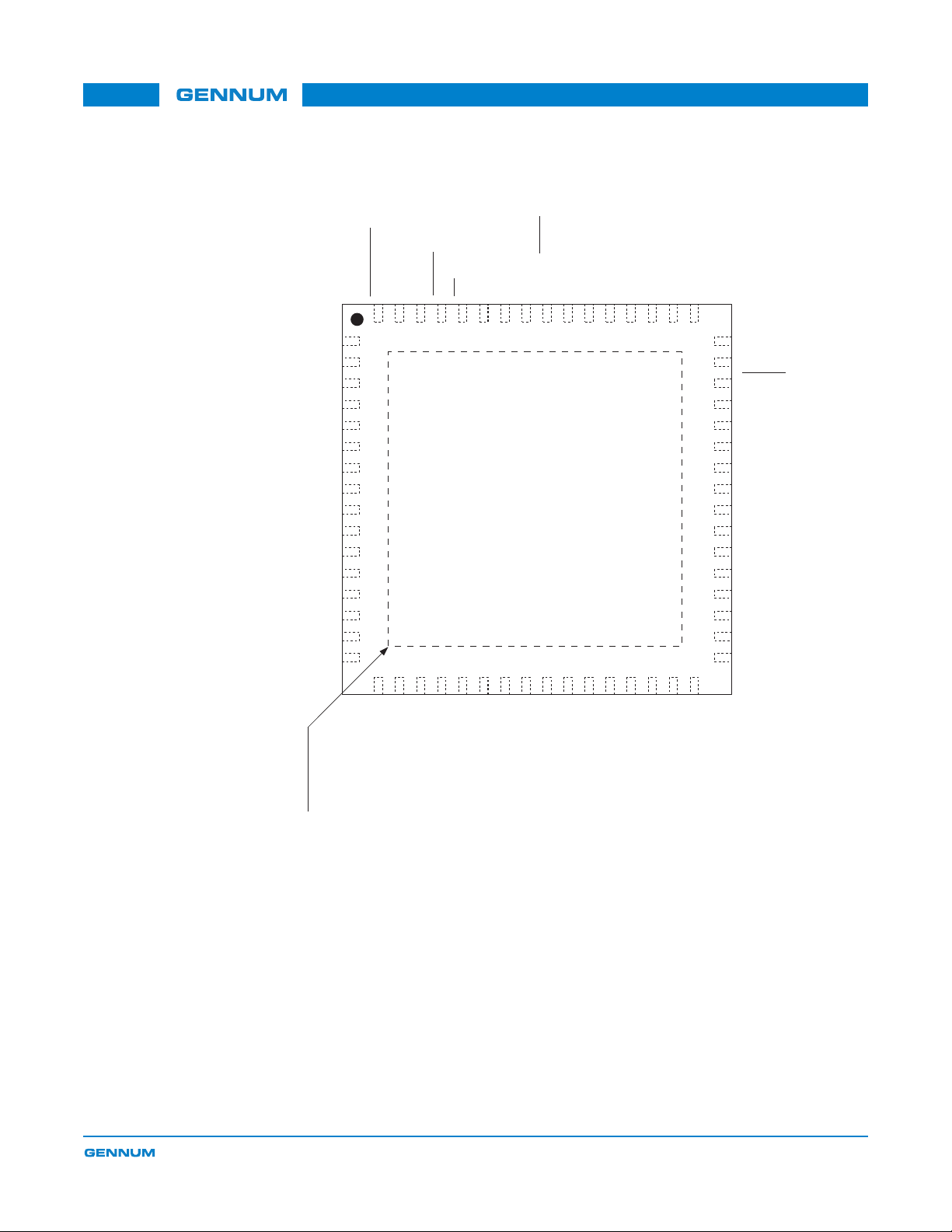
1.2 GS4910B Pin Assignment
LOCK_LOST
REF_LOST
VID_PLL_VDD
VID_PLL_GND
XTAL_VDD
X1
X2
XTAL_GND
CORE_GND
ANALOG_VDD
NC
ANALOG_GND
ANALOG_GND
ANALOG_GND
10FID
HSYNC
GENLOCK
NC
1
2
3
4
5
6
7
8
9
10
11
12
13
14
15
16
18 19 20 21 23 24 25 26 27 28 29 30 3122
17
IO_VDD
6263
61
RESET
CS_TMS
JTAG/HOST
SDIN_TDI
SCLK_TCLK
SDOUT_TDO
GS4910B
64-pin QFN
(Top View)
PhS_GND
PhS_VDD
PCLK1&2_VDD
GS4911B/GS4910B Data Sheet
PCLK1
IO_VDD
PCLK1&2_GND
PCLK2
4964
5051525354555657585960
32
LVDS/PCLK3_GND
48
PCLK3
47
PCLK3
46
LVDS/PCLK3_VDD
45
44
CORE_VDD
TIMING_OUT_8
43
TIMING_OUT_7
42
TIMING_OUT_6
41
TIMING_OUT_5
40
TIMING_OUT_4
39
IO_VDD
38
TIMING_OUT_3
37
TIMING_OUT_2
36
TIMING_OUT_1
35
34
ANALOG_GND
33
ANALOG_GND
Ground Pad
(bottom of package)
IO_VDD
VSYNC
FSYNC
NC
VID_STD0
VID_STD2
VID_STD1
CORE_VDD
VID_STD4
VID_STD3
NC
NC
VID_STD5
NC
IO_VDD
ANALOG_GND
36655 - 4 April 2007 9 of 113
1.3 Pin Descriptions
Table 1-1: Pin Descriptions
Pin Number Name Timing Type Description
GS4911B/GS4910B Data Sheet
1 LOCK_LOST Non
Synchronous
2 REF_LOST Non
Synchronous
3 VID_PLL_VDD – Power
4 VID_PLL_GND – Power
5 XTAL_VDD – Power
6X1 Non
Synchronous
7X2 Non
Synchronous
8XTAL_GND – Power
9 CORE_GND – Power
10 ANALOG_VDD – Power
11, 20, 63 NC – – Do not connect.
Output STATUS SIGNAL OUTPUT
Signal levels are LVCMOS/LVTTL compatible.
This pin will be HIGH if the output is not genlocked to the input.
The GS4911B/GS4910B monitors the output pixel/line counters, as well
as the internal lock status from the genlock block and asserts
LOCK_LOST HIGH if it is determined that the output is not genlocked to
the input. This pin will be LOW if the device successfully genlocks the
output clock and timing signals to the input reference.
If LOCK_LOST is LOW, the reference timing generator outputs will be
phase locked to the detected reference signal, producing an output in
accordance with the video standard selected by the VID_STD[5:0] pins.
Output STATUS SIGNAL OUTPUT
Signal levels are LVCMOS/LVTTL compatible.
This pin will be HIGH if:
• No input reference signal is applied to the device; or
• The input reference applied does not meet the minimum/maximum
timing requirements described in Section 3.5.2 on page 46.
This pin will be LOW otherwise.
If the reference signal is removed when the device is in Genlock mode,
REF_LOST will go HIGH and the GS4911B/GS4910B will enter Freeze
mode (see Section 3.2.1.2 on page 41).
Most positive power supply connection for the video clock synthesis
Supply
Supply
Supply
Input ANALOG SIGNAL INPUT
Output ANALOG SIGNAL OUTPUT
Supply
Supply
Supply
internal block. Connect to +1.8V DC.
Ground connection for the video clock synthesis internal block. Connect
to GND.
Most positive power supply connection for the crystal buffer. Connect to
either +1.8V DC or +3.3V DC.
NOTE: Connect to +3.3V for minimum output PCLK jitter.
Connect to a 27MHz crystal or a 27MHz external clock source. See
Figure 1-1.
Connect to a 27MHz crystal, or leave this pin open circuit if an external
clock source is applied to pin 6. See Figure 1-1.
Ground connection for the crystal buffer. Connect to GND.
Ground connection for core and I/O. Solder to the ground plane of the
application board.
NOTE: The CORE_GND pin should be soldered to the same main
ground plane as the exposed ground pad on the bottom of the device.
Most positive power supply connection for the analog input block.
Connect to +1.8V DC.
36655 - 4 April 2007 10 of 113
Table 1-1: Pin Descriptions (Continued)
Pin Number Name Timing Type Description
GS4911B/GS4910B Data Sheet
12 ANALOG_GND – Power
13 AUD_PLL_GND
14 AUD_PLL_VDD
15 10FID Non
16 HSYNC Non
17 VSYNC Non
18, 31, 38,
50, 62
(GS4911B only)
ANALOG_GND
(GS4910B only)
(GS4911B only)
ANALOG_GND
(GS4910B only)
IO_VDD – Power
– Power
– Power
– Power
– Power
Synchronous
Synchronous
Synchronous
Ground connection for the analog input block. Connect to GND.
Supply
Supply
Supply
Supply
Supply
Input REFERENCE SIGNAL INPUT
Input REFERENCE SIGNAL INPUT
Input REFERENCE SIGNAL INPUT
Supply
Ground connection for the audio clock synthesis internal block. Connect
to GND.
Ground connection for the analog input block. Connect to GND.
Most positive power supply connection for the audio clock synthesis
internal block. Connect to +1.8V DC.
Ground connection for the analog input block. Connect to GND.
Signal levels are LVCMOS/LVTTL compatible.
The 10FID external reference signal is applied to this pin by the
application layer. 10FID defines the field in which the video and audio
clock phase relationship is defined according to SMPTE 318-M. It is also
used to define a 3:2 video cadence.
NOTE: If the input reference format does not include a 10 Field ID signal,
this pin should be held LOW. See Section 3.4.2 on page 45.
Signal levels are LVCMOS/LVTTL compatible.
The HSYNC external reference signal is applied to this pin by the
application layer. When the GS4911B/GS4910B is operating in Genlock
mode, the device senses the polarity of the HSYNC input automatically,
and references to the leading edge.
If the user wishes to select one of the pre-programmed video and/or
timing output signals provided by the device, then this signal must
adhere to one of the 36 defined video or 16 different graphics display
standards supported by the device. In this mode of operation, the
HSYNC input provides a horizontal scanning reference signal.
The HSYNC signal may have analog timing, such as from a sync
separator, or may be digital such as from an SDI deserializer. Section 1.4
on page 20 describes the 36 video formats and 16 graphic formats
recognized by the GS4911B/GS4910B.
Signal levels are LVCMOS/LVTTL compatible.
The VSYNC external reference signal is applied to this pin by the
application layer. When the GS4911B/GS4910B is operating in Genlock
mode, the device senses the polarity of the VSYNC input automatically,
and references to the leading edge.
If the user wishes to select one of the pre-programmed video and/or
timing output signals provided by the device, then this signal must
adhere to one of the 36 defined video or 16 different graphics display
standards supported by the device. In this mode of operation, the
VSYNC input provides a vertical scanning reference signal.
The VSYNC signal may have analog timing, such as from a sync
separator, or may be digital such as from an SDI deserializer. Section 1.4
on page 20 describes the 36 video formats and 16 graphic formats
recognized by the GS4911B/GS4910B.
Most positive power supply connection for the digital I/O signals.
Connect to either +1.8V DC or +3.3V DC.
NOTE: All five IO_VDD pins must be powered by the same voltage.
36655 - 4 April 2007 11 of 113

Table 1-1: Pin Descriptions (Continued)
Pin Number Name Timing Type Description
GS4911B/GS4910B Data Sheet
19 FSYNC Non
Synchronous
27, 25, 24,
23, 22, 21
26, 44 CORE_VDD – Power
VID_STD[5:0] Non
Synchronous
Input REFERENCE SIGNAL INPUT
Input CONTROL SIGNAL INPUTS
Supply
Signal levels are LVCMOS/LVTTL compatible.
The FSYNC external reference signal is applied to this pin by the
application layer.
The first field is defined as the field in which the first broad pulse (also
known as serration) is in the first half of a line. The FSYNC signal should
be set HIGH during the first field for sync-based references.
If the user wishes to select one of the pre-programmed video and/or
timing output signals provided by the device, then this signal must
adhere to one of the 36 defined video or 16 different graphics display
standards supported by the device. In this mode of operation, the
FSYNC input provides an odd/even field input reference.
The FSYNC signal may have analog timing, such as from a sync
separator, or may be digital such as from an SDI deserializer. Section 1.4
on page 20 describes the 36 video formats and 16 graphic formats
recognized by the GS4911B/GS4910B.
For blanking-based references, the FSYNC signal should be set HIGH
during the second field.
NOTE: If the input reference format does not include an F sync signal,
this pin should be held LOW.
Signal levels are LVCMOS/LVTTL compatible.
Video Standard Select.
Used to select the desired video/graphic display format for video clock
and timing signal generation.
8 different video and 13 different graphic sample clocks, as well as 35
different video format and 13 different graphic format timing signal
outputs may be selected using these pins.
For details on the supported video standards and video clock frequency
selection, please see Section 1.4 on page 20.
Most positive power supply connection for the digital core. Connect to
+1.8V DC.
36655 - 4 April 2007 12 of 113

Table 1-1: Pin Descriptions (Continued)
Pin Number Name Timing Type Description
GS4911B/GS4910B Data Sheet
28, 29, 30 ACLK1
ACLK2
ACLK3
(GS4911B only)
NC
(GS4910B only)
32, 33, 34 ASR_SEL[2:0]
(GS4911B only)
ANALOG_GND
(GS4910B only)
35 TIMING_OUT_1 Synchronous
– Output CLOCK SIGNAL OUTPUTS
– – Do not connect.
Non
Synchronous
– Power
with PCLK1 ~
PCLK3
Signal levels are LVCMOS/LVTTL compatible.
Audio output clock signals.
ACLK1, ACLK2, and ACLK3 present audio sample rate clock outputs to
the application layer.
By default, after system reset, the audio clock output pins of the device
provide clock signals as follows:
ACLK1 = 256fs
ACLK2 = 64fs
ACLK3 = fs, where fs is the fundamental sampling frequency.
The fundamental sampling frequency is selected using ASR_SEL[2:0].
Additional sampling frequencies may be programmed in the host
interface.
It is also possible to select different division ratios for each of the audio
clock outputs by programming designated registers in the host interface.
Clock outputs of 512fs, 384fs, 256fs, 192fs, 128fs, 64fs, fs and z bit are
selectable on a pin-by-pin basis.
NOTE: ACLK1-3 will have a 50% duty cycle, unless fs is selected as
96kHz and the host interface is configured such that one of the three
ACLK pins is set to output a clock signal at 192fs or 384fs. If this is the
case, then a 512fs clock will have a 33% duty cycle.
These signals will be high impedance when ASR_SEL[2:0] = 000b.
Input CONTROL SIGNAL INPUTS
Signal levels are LVCMOS/LVTTL compatible.
Audio Sample Rate Select.
Used to select the fundamental sampling frequency, fs, of the audio clock
outputs. See Table 3-7.
When ASR_SEL[2:0] = 000b, audio clock generation will be disabled and
the ACLK1 to ACLK3 pins will be high impedance. In this case,
AUD_PLL_VDD (pin 14) may be connected to GND to minimize noise
and power consumption.
Ground connection for the analog input block. Connect to GND.
Supply
Output TIMING SIGNAL OUTPUT
Signal levels are LVCMOS/LVTTL compatible.
Selectable timing output.
Selectable from: H sync; H blanking; V sync; V blanking; F sync; F
digital; Display Enable; 10 field ID (film cadence); AFS video/audio timing
(GS4911B only); USER_1~4.
See Section 1.5 on page 26 for signal descriptions.
NOTE: Default output is H Sync.
The current drive capability of this pin may be set high or low via
designated registers in the host interface. By default, the current drive
will be low.
This signal will be high impedance when VID_STD[5:0] = 00h.
36655 - 4 April 2007 13 of 113

Table 1-1: Pin Descriptions (Continued)
Pin Number Name Timing Type Description
GS4911B/GS4910B Data Sheet
36 TIMING_OUT_2 Synchronous
with PCLK1 ~
PCLK3
37 TIMING_OUT_3 Synchronous
with PCLK1 ~
PCLK3
39 TIMING_OUT_4 Synchronous
with PCLK1 ~
PCLK3
40 TIMING_OUT_5 Synchronous
with PCLK1 ~
PCLK3
Output TIMING SIGNAL OUTPUT
Signal levels are LVCMOS/LVTTL compatible.
Selectable timing output.
Selectable from: H sync; H blanking; V sync; V blanking; F sync; F
digital; Display Enable; 10 field ID (film cadence); AFS video/audio timing
(GS4911B only); USER_1~4.
See Section 1.5 on page 26 for signal descriptions.
NOTE: Default output is H blanking.
The current drive capability of this pin may be set high or low via
designated registers in the host interface. By default, the current drive
will be low.
This signal will be high impedance when VID_STD[5:0] = 00h.
Output TIMING SIGNAL OUTPUT
Signal levels are LVCMOS/LVTTL compatible.
Selectable timing output.
Selectable from: H sync; H blanking; V sync; V blanking; F sync; F
digital; Display Enable; 10 field ID (film cadence); AFS video/audio timing
(GS4911B only); USER_1~4.
See Section 1.5 on page 26 for signal descriptions.
NOTE: Default output is V Sync.
The current drive capability of this pin may be set high or low via
designated registers in the host interface. By default, the current drive
will be low.
This signal will be high impedance when VID_STD[5:0] = 00h.
Output TIMING SIGNAL OUTPUT
Signal levels are LVCMOS/LVTTL compatible.
Selectable timing output.
Selectable from: H sync; H blanking; V sync; V blanking; F sync; F
digital; Display Enable; 10 field ID (film cadence); AFS video/audio timing
(GS4911B only); USER_1~4.
See Section 1.5 on page 26 for signal descriptions.
NOTE: Default output is V blanking.
The current drive capability of this pin may be set high or low via
designated registers in the host interface. By default, the current drive
will be low.
This signal will be high impedance when VID_STD[5:0] = 00h.
Output TIMING SIGNAL OUTPUT
Signal levels are LVCMOS/LVTTL compatible.
Selectable timing output.
Selectable from: H sync; H blanking; V sync; V blanking; F sync; F
digital; Display Enable; 10 field ID (film cadence); AFS video/audio timing
(GS4911B only); USER_1~4.
See Section 1.5 on page 26 for signal descriptions.
NOTE: Default output is F Sync.
The current drive capability of this pin may be set high or low via
designated registers in the host interface. By default, the current drive
will be low.
This signal will be high impedance when VID_STD[5:0] = 00h.
36655 - 4 April 2007 14 of 113

Table 1-1: Pin Descriptions (Continued)
Pin Number Name Timing Type Description
GS4911B/GS4910B Data Sheet
41 TIMING_OUT_6 Synchronous
with PCLK1 ~
PCLK3
42 TIMING_OUT_7 Synchronous
with PCLK1 ~
PCLK3
43 TIMING_OUT_8 Synchronous
with PCLK1 ~
PCLK3
45 LVDS/PCLK3_VDD – Power
Output TIMING SIGNAL OUTPUT
Output TIMING SIGNAL OUTPUT
Output TIMING SIGNAL OUTPUT
Supply
Signal levels are LVCMOS/LVTTL compatible.
Selectable timing output.
Selectable from: H sync; H blanking; V sync; V blanking; F sync; F
digital; Display Enable; 10 field ID (film cadence); AFS video/audio timing
(GS4911B only); USER_1~4.
See Section 1.5 on page 26 for signal descriptions.
NOTE: Default output is F digital.
The current drive capability of this pin may be set high or low via
designated registers in the host interface. By default, the current drive
will be low.
This signal will be high impedance when VID_STD[5:0] = 00h.
Signal levels are LVCMOS/LVTTL compatible.
Selectable timing output.
Selectable from: H sync; H blanking; V sync; V blanking; F sync; F
digital; Display Enable; 10 field ID (film cadence); AFS video/audio timing
(GS4911B only); USER_1~4.
See Section 1.5 on page 26 for signal descriptions.
NOTE: Default output is 10 Field ID (10FID).
The current drive capability of this pin may be set high or low via
designated registers in the host interface. By default, the current drive
will be low.
This signal will be high impedance when VID_STD[5:0] = 00h.
Signal levels are LVCMOS/LVTTL compatible.
Selectable timing output.
Selectable from: H sync; H blanking; V sync; V blanking; F sync; F
digital; Display Enable; 10 field ID (film cadence); AFS video/audio timing
(GS4911B only); USER_1~4.
See Section 1.5 on page 26 for signal descriptions.
NOTE: Default output is Display Enable (DE).
The current drive capability of this pin may be set high or low via
designated registers in the host interface. By default, the current drive
will be low.
This signal will be high impedance when VID_STD[5:0] = 00h.
Most positive power supply connection for PCLK3 output circuitry and
LVDS driver. Connect to +1.8V DC.
36655 - 4 April 2007 15 of 113
Table 1-1: Pin Descriptions (Continued)
Pin Number Name Timing Type Description
GS4911B/GS4910B Data Sheet
46, 47 PCLK3
, PCLK3 – Output CLOCK SIGNAL OUTPUTS
Signal levels are LVDS compatible.
Differential video clock output signal.
PCLK3/PCLK3 present a differential video sample rate clock output to
the application layer.
By default, after system reset, this output will operate at the fundamental
frequency determined by the setting of the VID_STD[5:0] pins. It is
possible to define other non-standard fundamental clock rates using the
host interface.
It is also possible to select different division ratios for the
PCLK3/PCLK3 outputs by programming designated registers in the
host interface. A clock output of the fundamental rate, fundamental rate
÷2, or fundamental rate ÷4 may be selected.
The
PCLK3/PCLK3 outputs will be high impedance when
VID_STD[5:0] = 00h.
48 LVDS/PCLK3_GND – Power
Supply
49 PCLK2 – Output CLOCK SIGNAL OUTPUT
51 PCLK1 – Output CLOCK SIGNAL OUTPUT
Ground connection for PCLK3 output circuitry and LVDS driver. Connect
to GND.
Signal levels are LVCMOS/LVTTL compatible.
Video clock output signal.
PCLK2 presents a video sample rate clock output to the application
layer.
By default, after system reset, the PCLK2 output pin will operate at the
fundamental frequency determined by the setting of the VID_STD[5:0]
pins. It is possible to define other non-standard fundamental clock rates
using the host interface.
It is also possible to select different division ratios for the PCLK2 output
by programming designated registers in the host interface. A clock
output of the fundamental rate, fundamental rate ÷2, or fundamental rate
÷4 may be selected.
By setting designated registers in the host interface, the current drive
capability of this pin may be set high or low. By default, the current drive
will be low. It must be set high if the clock rate is greater than 100MHz.
The PCLK2 output will be held LOW when VID_STD[5:0] = 00h.
Signal levels are LVCMOS/LVTTL compatible.
Video clock output signal.
PCLK1 presents a video sample rate clock output to the application
layer.
By default, after system reset, the PCLK1 output pin will operate at the
fundamental frequency determined by the setting of the VID_STD[5:0]
pins. It is possible to define other non-standard fundamental clock rates
using the host interface.
It is also possible to select different division ratios for the PCLK1 output
by programming designated registers in the host interface. A clock
output of the fundamental rate, fundamental rate ÷2, or fundamental rate
÷4 may be selected.
By setting designated registers in the host interface, the current drive
capability of this pin may be set high or low. By default, the current drive
will be low. It must be set high if the clock rate is greater than 100MHz.
The PCLK1 output will be held LOW when VID_STD[5:0] = 00h.
36655 - 4 April 2007 16 of 113
Table 1-1: Pin Descriptions (Continued)
Pin Number Name Timing Type Description
GS4911B/GS4910B Data Sheet
52 PCLK1&2_GND – Power
Supply
53 PCLK1&2_VDD – Power
54 PhS_VDD – Power
55 PhS_GND – Power
56 JTAG/HOST
57 SCLK_TCLK Non
58 SDIN_TDI Synchronous
59 SDOUT_TDO Synchronous
Non
Synchronous
Synchronous
with
SCLK_TCLK
with
SCLK_TCLK
Supply
Supply
Supply
Input CONTROL SIGNAL INPUT
Input SIGNAL INPUT
Input SIGNAL INPUT
Output SIGNAL INPUT
Ground connection for PCLK1&2 circuitry. Connect to GND.
Most positive power supply connection for PCLK1&2 circuitry. Connect to
+1.8V DC.
Most positive power supply connection for the video clock phase shift
internal block. Connect to +1.8V DC.
Ground connection for the video clock phase shift internal block. Connect
to GND.
Signal levels are LVCMOS/LVTTL compatible.
Used to select JTAG Test Mode or Host Interface Mode.
When set HIGH, CS
are configured for JTAG boundary scan testing.
When set LOW, CS_TMS, SCLK_TCLK, SDOUT_TDO, and SDIN_TDI
are configured as GSPI pins for normal host interface operation.
Signal levels are LVCMOS/LVTTL compatible.
Serial Data Clock / Test Clock.
All JTAG / Host Interface address and data are shifted into/out of the
device synchronously with this clock.
Host Mode (JTAG/HOST
SCLK_TCLK operates as the host interface serial data clock, SCLK.
JTAG Test Mode (JTAG/HOST = HIGH):
SCLK_TCLK operates as the JTAG test clock, TCLK.
Signal levels are LVCMOS/LVTTL compatible.
Serial Data Input / Test Data Input.
Host Mode (JTAG/HOST
SDIN_TDI operates as the host interface serial input, SDIN, used to write
address and configuration information to the internal registers of the
device.
JTAG Test Mode (JTAG/HOST
SDIN_TDI operates as the JTAG test data input, TDI.
Signal levels are LVCMOS/LVTTL compatible.
Serial Data Output / Test Data Output.
Host Mode (JTAG/HOST
SDOUT_TDO operates as the host interface serial output, SDOUT, used
to read status and configuration information from the internal registers of
the device.
JTAG Test Mode (JTAG/HOST
SDOUT_TDO operates as the JTAG test data output, TDO.
_TMS, SCLK_TCLK, SDOUT_TDO, and SDIN_TDI
= LOW):
= LOW):
= HIGH):
= LOW):
= HIGH):
36655 - 4 April 2007 17 of 113
Table 1-1: Pin Descriptions (Continued)
Pin Number Name Timing Type Description
GS4911B/GS4910B Data Sheet
60 CS
61 RESET
64 GENLOCK
– Ground Pad – – Ground pad on bottom of package must be soldered to main ground
_TMS Synchronous
with
SCLK_TCLK
Non
Synchronous
Non
Synchronous
Input SIGNAL INPUT
Signal levels are LVCMOS/LVTTL compatible.
Chip Select / Test Mode Select.
Host Mode (JTAG/HOST
CS
_TMS operates as the host interface chip select, CS, and is active
LOW.
JTAG Test Mode (JTAG/HOST
CS
_TMS operates as the JTAG test mode select, TMS, and is active
HIGH.
Input CONTROL SIGNAL INPUT
Signal levels are LVCMOS/LVTTL compatible.
Used to reset the internal operating conditions to their default settings or
to reset the JTAG test sequence.
Host Mode (JTAG/HOST
When asserted LOW, all host registers and functional blocks will be set
to their default conditions. All input and output signals will become high
impedance, except PCLK1 and PCLK2, which will be set LOW.
When set HIGH, normal operation of the device will resume.
The user must hold this pin LOW during power-up and for a minimum of
500 uS after the last supply has reached its operating voltage.
JTAG Test Mode (JTAG/HOST
When asserted LOW, all host registers and functional blocks will be set
to their default conditions and the JTAG test sequence will be held in
reset.
When set HIGH, normal operation of the JTAG test sequence will
resume.
Input CONTROL SIGNAL INPUT
Signal levels are LVCMOS/LVTTL compatible.
Selects Genlock mode or Free Run mode.
When this pin is set LOW and the device has successfully genlocked the
output to the input reference, the device will enter Genlock mode. The
video clock and timing outputs will be frequency and phase locked to the
detected reference signal.
When this pin is set HIGH, the video clock and the reference-timing
generator will free-run.
By default, the GS4911B’s audio clocks will be genlocked to the output
video clock regardless of the setting of this pin.
NOTE: The user must apply a reference to the input of the device prior to
setting GENLOCK
reference signal is present, the generated clock and timing outputs of the
device may correspond to the internal default settings of the chip until a
reference is applied.
plane of PCB.
= LOW):
= LOW):
= LOW. If the GENLOCK pin is set LOW and no
= HIGH):
= HIGH):
36655 - 4 April 2007 18 of 113
GS4911B/GS4910B Data Sheet
External Crystal Connection External Clock Source Connection
38pF
1M
24pF
6
X1
external
clock
7
X2
Notes:
1. Capacitor values listed represent the total capacitance,
including discrete capacitance and parasitic board capacitance.
2. X1 serves as an input, which may alternatively accept a 27MHz clock
source. To accomodate this, mismatched capacitor values are recommended.
Figure 1-1: XTAL1 and XTAL2 Reference Circuits
NC
6
X1
7
X2
36655 - 4 April 2007 19 of 113

1.4 Pre-Programmed Recognized Video and Graphics Standards
Table 1-2 describes the video and graphics standards automatically recognized by
the GS4911B/GS4910B. Any one of the 36 different video formats and 16 different
graphic display formats listed below can be applied to the GS4911B/GS4910B and
automatically detected by the reference format detector. Moreover, each format,
with the exception of VID_STD[5:0] = 2, 52, 53, or 54, is available for output on the
timing output pins by setting the VID_STD[5:0] pins.
In addition to the pre-programmed video standards listed in Table 1-2, custom
output timing signals may be generated by the GS4911B/GS4910B. The custom
timing parameters are programmed in the host interface when VID_STD[5:0] is set
to 62 (see Section 3.10 on page 75).
Setting VID_STD[5:0] to 63 will cause the device to produce an output format with
identical timing to the detected input reference.
If desired, the external VID_STD[5:0] pins may be ignored by setting bit 1 of the
Video_Control register, and the video standard may instead be selected via the
VID_STD[5:0] register of the host interface (see Section 3.12.3 on page 80).
Although the external VID_STD[5:0] pins will be ignored in this case, they should
not be left floating.
GS4911B/GS4910B Data Sheet
36655 - 4 April 2007 20 of 113

GS4911B/GS4910B Data Sheet
Standard
Scan Format
Active
Lines /
V Sync
Polarity
Width
V Sync
H Sync
Polarity
Width
H Sync
Active
PCLKS /
Frame
(Lines)
(Clocks)
Line
125M/267M
/ SMPTE 347M
/ SMPTE 347M
/ SMPTE 347M
21 of 113
/ SMPTE 347M
Table 1-2: Recognized Video and Graphics Standards
Frame
Total Lines /
/ Total
PCLKS
Frequency
Video PCLK
System
Nomenclature
[5:0]
VID_STD
Line
––––––––––
(MHz)
= High
PCLK3/PCLK3
0 PCLK1&2 =LOW.
14.32 910 525 768 67 negative 3 negative 486 SMPTE 244M
Impedance
interlace
1 4fsc 525 / 2:1
– – 625 – – negative 2.5 negative 576 –
/ 2:1 interlace / 25
3 601 525 / 2:1 interlace 27 1716 525 1440 127 negative 3 negative 486 SMPTE
2* Composite PAL 625
4‡ 601 625 / 2:1 interlace 27 1728 625 1440 127 negative 2.5 negative 576 ITU-R BT.601-5
36 2288 525 1920 169 negative 3 negative 486 SMPTE 267M
36 2304 625 1920 169 negative 2.5 negative 576 ITU-R BT.601-5
/ 2:1 interlace
5 601 – 18MHz 525
6‡ 601 – 18 MHz 625
54 3432 525 2880 252 negative 3 negative 486 SMPTE RP174
/ 2:1 interlace
interlace
7 720x486/59.94/2:1
54 3456 625 2880 252 negative 2.5 negative 576 ITU-R BT.799
8‡ 720x576/50/2:1
interlace
54 1716 525 1440 127 negative 6 negative 483 SMPTE 293M
9 720x483/59.94/1:1
progressive
54 1728 625 1440 127 negative 5 negative 576 ITU-R BT.1358
progressive
10 720x576/50/1:1
74.25 1650 750 1280 80 tri 5 negative 720 SMPTE 296M
11 1280x720/60/1:1
progressive
74.175 1650 750 1280 80 tri 5 negative 720 SMPTE 296M
12 1280x720/59.94/1:1
progressive
74.25 1980 750 1280 80 tri 5 negative 720 SMPTE 296M
36655 - 4 April 2007
progressive
13 1280/720/50/1:1
GS4911B/GS4910B Data Sheet
Standard
Scan Format
Active
Lines /
V Sync
Polarity
Width
V Sync
H Sync
Polarity
Width
H Sync
Active
PCLKS /
22 of 113
Frame
(Lines)
(Clocks)
Line
Frame
Total Lines /
Line
/ Total
PCLKS
74.25 3300 750 1280 80 tri 5 negative 720 SMPTE 296M
(MHz)
Frequency
Video PCLK
System
Nomenclature
[5:0]
VID_STD
Table 1-2: Recognized Video and Graphics Standards (Continued)
progressive
14 1280x720/30/1:1
74.175 3300 750 1280 80 tri 5 negative 720 SMPTE 296M
15 1280x720/29.97/1:1
progressive
74.25 3960 750 1280 80 tri 5 negative 720 SMPTE 296M
16 1280x720/25/1:1
progressive
74.25 4125 750 1280 80 tri 5 negative 720 SMPTE 296M
17 1280x720/24/1:1
progressive
74.175 4125 750 1280 80 tri 5 negative 720 SMPTE 296M
18 1280x720/23.98/1:1
progressive
74.25 2200 1125 1920 80 tri 5 negative 1035 SMPTE 260M
19 1920x1035/60/2:1
interlace
74.175 2200 1125 1920 80 tri 5 negative 1035 SMPTE 260M
interlace
20 1920x1035/59.94/2:1
148.5 2200 1125 1920 80 tri 5 negative 1080 SMPTE 274M
21 1920x1080/60/1:1
progressive
148.35 2200 1125 1920 80 tri 5 negative 1080 SMPTE 274M
progressive
22 1920x1080/59.94/1:1
148.5 2640 1125 1920 80 tri 5 negative 1080 SMPTE 274M
23 1920x1080/50/1:1
progressive
74.25 2200 1125 1920 80 tri 5 negative 1080 SMPTE 274M
interlace
24 Reserved – – – – – – – – – –
25 1920x1080/60/2:1
74.175 2200 1125 1920 80 tri 5 negative 1080 SMPTE 274M
interlace
26 1920x1080/59.94/2:1
74.25 2640 1125 1920 80 tri 5 negative 1080 SMPTE 274M
27 1920x1080/50/2:1
36655 - 4 April 2007
interlace
28 Reserved – – – – – – – – – –
GS4911B/GS4910B Data Sheet
Standard
Scan Format
Active
Lines /
V Sync
Polarity
Width
V Sync
H Sync
Polarity
Width
H Sync
Active
PCLKS /
Frame
(Lines)
(Clocks)
Line
VDMT75HZ
VDMTPROP
VG900602
VDMT75HZ
VDMTPROP
VG901101A
23 of 113
Frame
Total Lines /
Line
/ Total
PCLKS
74.25 2200 1125 1920 80 tri 5 negative 1080 SMPTE 274M
(MHz)
Frequency
Video PCLK
System
Nomenclature
[5:0]
VID_STD
Table 1-2: Recognized Video and Graphics Standards (Continued)
progressive
29 1920x1080/30/1:1
74.175 2200 1125 1920 80 tri 5 negative 1080 SMPTE 274M
progressive
30 1920x1080/30/PsF 74.25 2200 1125 1920 80 tri 5 negative 1080 SMPTE RP 211
31 1920x1080/29.97/1:1
74.25 2640 1125 1920 80 tri 5 negative 1080 SMPTE 274M
progressive
32 1920x1080/29.97/PsF 74.175 2200 1125 1920 80 tri 5 negative 1080 SMPTE RP 211
33 1920x1080/25/1:1
74.25 2750 1125 1920 80 tri 5 negative 1080 SMPTE 274M
progressive
34 1920x1080/25/PsF 74.25 2640 1125 1920 80 tri 5 negative 1080 SMPTE RP 211
35 1920x1080/24/1:1
74.175 2750 1125 1920 80 tri 5 negative 1080 SMPTE 274M
progressive
36 1920x1080/24/PsF 74.25 2750 1125 1920 80 tri 5 negative 1080 SMPTE RP 211
37 1920x1080/23.98/1:1
25.2 800 525 640 96 negative 2 negative 480 IBM Standard
@ 60 Hz
38 1920x1080/23.98/PsF 74.175 2750 1125 1920 80 tri 5 negative 1080 SMPTE RP 211
39 640 x 480 VGA
36 832 509 640 56 negative 3 negative 480 VESA
31.5 840 500 640 64 negative 3 negative 480 VESA
@ 75 Hz
@ 85 Hz
40 640 x 480 VGA
41 640 x 480 VGA
49.5 1056 625 800 80 positive 3 positive 600 VESA
40.00 1056 628 800 128 positive 4 positive 600 VESA
@ 60 Hz
@ 75 Hz
42 800 x 600 SVGA
43 800 x 600 SVGA
65 1344 806 1024 136 negative 6 negative 768 VESA
56.25 1048 631 800 64 positive 3 positive 600 VESA
@ 85 Hz
@ 60 Hz
44 800 x 600 SVGA
45 1024 x 768 XGA
36655 - 4 April 2007

GS4911B/GS4910B Data Sheet
Standard
Scan Format
Active
Lines /
V Sync
Polarity
Width
V Sync
H Sync
Polarity
Width
H Sync
Active
PCLKS /
Frame
(Lines)
(Clocks)
Line
VDMT75HZ
VDMTPROP
VDMTREV
VDMT75HZ
VDMTPROP
VDMTPROP
24 of 113
Frame
Total Lines /
Line
/ Total
PCLKS
– – 1250 – – negative 3 positive 1200 –
– – 1250 – – negative 3 positive 1200 –
94.5 1376 808 1024 96 negative 3 positive 768 VESA
78.75 1312 800 1024 96 positive 3 positive 768 VESA
(MHz)
Frequency
Video PCLK
System
Nomenclature
[5:0]
VID_STD
Table 1-2: Recognized Video and Graphics Standards (Continued)
@ 75 Hz
46 1024 x 768 XGA
108.00 1688 1066 1280 112 positive 3 positive 1024 VESA
@ 85 Hz
@ 60 Hz
47 1024 x 768 XGA
48 1280 x 1024 SXGA
135.00 1688 1066 1280 144 negative 3 positive 1024 VESA
@ 75 Hz
49 1280 x 1024 SXGA
162 2160 1250 1600 192 negative 3 positive 1200 VESA
157.5 1728 1072 1280 160 negative 3 positive 1024 VESA
@ 85 Hz
@ 60 Hz
@ 75 Hz
50 1280 x 1024 SXGA
51† 1600 x 1200 UXGA
52* 1600 x 1200 UXGA
– – 1589 – – negative 3 positive 1536 –
@ 85 Hz
@ 60 Hz
53* 1600 x 1200 UXGA
54* 2048 x 1536 QXGA
––––––––––
(Section 3.10 on
62 Custom format only
55 - 61 Reserved – – – – – – – – – –
––––––––––
page 75)
Standard follows Input
Standard
63 Automatic Output
36655 - 4 April 2007
* VID_STD[5:0] = 2, 52, 53, and 54 are recognized as input references only. To generate clock and timing signals for these standards use the device’s custom format capability.
† The LOCK_LOST output signal will be unstable when attempting to genlock to an input reference corresponding to VID_STD[5:0] = 51, although the device does achieve lock. To correct
this, the user can program register address 27h = 38d.
‡ When VID_STD = 4, 6, or 8, the Vblanking output pulse width is 2 lines too long for field 1 and 1 line too short for field 2 when compared to the digital timing defined in ITU-R BT.656 and
ITU-R BT.799.
GS4911B/GS4910B Data Sheet
1.5 Output Timing Signals
Table 1-3 describes the output timing signals available to the user via pins
TIMING_OUT_1 to TIMING_OUT_8. The user may output any of the signals listed
below on each pin by programming the Output_Select registers beginning at
address 43h of the host interface.
s
Table 1-3: Output Timing Signals
Signal Name Description Default Output Pin
H Sync The H Sync signal has a leading edge at the start of the horizontal sync pulse.
H Blanking The H Blanking signal is used to indicate the portion of the video line not
Its length is determined by the selected video standard (see Table 1-2), or
according to custom timing parameters programmed in the host interface (see
Section 3.10 on page 75).
The width of the H Sync output pulse is determined by the selected video
standard. Table 1-2
video and graphics standard recognized by the GS4911B/GS4910B. Custom
video timing parameters may also be programmed in the host interface to
define a unique H Sync width (see Section 3.10 on page 75).
In Genlock mode the leading edge of the output H Sync signal is nominally
simultaneous with the half amplitude point of the reference HSYNC input. This
timing may be offset using the Genlock Offset registers beginning at address
1Bh of the host interface (see Section 3.2.1.1 on page 38).
By default, after system reset, the polarity of the H Sync signal output will be
active LOW. The polarity may be selected as active HIGH by programming the
Polarity register at address 56h of the host interface (see Section 3.12.3 on
page 80).
containing active video data.
The H Blanking signal will be LOW (default polarity) for the portion of the video
line containing valid video samples. The signal will be LOW at the first valid
pixel of the line, and HIGH after the last valid pixel of the line.
The H Blanking signal remains HIGH throughout the horizontal blanking period.
The width of this signal will be determined by the selected video standard (see
Table 1-2), or according to custom timing parameters programmed in the host
interface (see Section 3.10 on page 75).
When in Genlock mode, the output H Blanking signal will be phase locked to the
reference HSYNC input. This timing may be offset using the Genlock Offset
registers beginning at address 1Bh of the host interface (see Section 3.2.1.1 on
page 38).
The default polarity of this signal may be inverted by programming the Polarity
register at address 56h of the host interface (see Section 3.12.3 on page 80).
lists the H Sync width (in clocks) of each pre-programmed
TIMING_OUT_1
TIMING_OUT_2
36655 - 4 April 2007 25 of 113

GS4911B/GS4910B Data Sheet
Table 1-3: Output Timing Signals (Continued)
Signal Name Description Default Output Pin
V Sync The V Sync timing signal has a leading edge at the start of the vertical sync
pulse. Its length is determined by the selected video standard (see Table 1-2),
or according to custom timing parameters programmed in the host interface
(see Section 3.10 on page 75).
The leading edge of V Sync is nominally simultaneous with the leading edge of
the first broad pulse.
When in Genlock mode, the output V Sync signal will be phase locked to the
reference VSYNC input. This timing may be offset using the Genlock Offset
registers beginning at address 1Bh of the host interface (see Section 3.2.1.1 on
page 38).
By default, after system reset, the polarity of the V Sync signal output will be
active LOW. The polarity may be selected as active HIGH by programming the
Polarity register at address 56h of the host interface (see Section 3.12.3 on
page 80).
V Blanking The V Blanking signal is used to indicate the portion of the video field/frame not
containing active video lines.
The V Blanking signal will be LOW (default polarity) for the portion of the
field/frame containing valid video data, and will be HIGH throughout the vertical
blanking period.
The width of this signal will be determined by the selected video standard (see
Table 1-2), or according to custom timing parameters programmed in the host
interface (see Section 3.10 on page 75).
When in Genlock mode, the output V Blanking signal will be phase locked to the
reference VSYNC input. This timing may be offset using the Genlock Offset
registers beginning at address 1Bh of the host interface (see Section 3.2.1.1 on
page 38).
The default polarity of this signal may be inverted by programming the Polarity
register at address 56h of the host interface (see Section 3.12.3 on page 80).
NOTE: When VID_STD = 4, 6, or 8, the Vblank output pulse width is 2 lines too
long for field 1 and 1 line too short for field 2 when compared to the digital timing
defined in ITU-R BT.656 and ITU-R BT.799.
F Sync The F Sync signal is used to indicate field 1 and field 2 for interlaced video
formats.
The F Sync signal will be HIGH (default polarity) for the entire period of field 1. It
will be LOW for all lines in field 2 and for all lines in progressive scan systems.
The width and timing of this signal will be determined by the V Sync parameters
of the selected video standard (see Table 1-2), or according to custom V Sync
timing parameters programmed in the host interface (see Section 3.10 on
page 75). The F Sync signal always changes state on the leading edge of V
Sync.
When in Genlock mode, the output F Sync signal will be phase locked to the
reference FSYNC input. This timing may be offset using the Genlock Offset
registers beginning at address 1Bh of the host interface (see Section 3.2.1.1 on
page 38).
The default polarity of this signal may be inverted by programming the Polarity
register at address 56h of the host interface (see Section 3.12.3 on page 80).
TIMING_OUT_3
TIMING_OUT_4
TIMING_OUT_5
36655 - 4 April 2007 26 of 113

GS4911B/GS4910B Data Sheet
Table 1-3: Output Timing Signals (Continued)
Signal Name Description Default Output Pin
F Digital F Digital is used in digital interlaced standards to indicate field 1 and field 2.
The F Digital changes state at the leading edge of every V Blanking pulse. It will
be LOW (default polarity) for the entire period of field 1 and for all lines in
progressive scan systems. It will be HIGH for all lines in field 2 .
The width and timing of this signal will be determined by the timing parameters
of the selected video standard (see Table 1-2), or according to custom
parameters programmed in the host interface (see Section 3.10 on page 75).
When in Genlock mode, the output F Digital signal will be phase locked to the
reference FSYNC input. This timing may be offset using the Genlock Offset
registers beginning at address 1Bh of the host interface (see Section 3.2.1.1 on
page 38).
The default polarity of this signal may be inverted by programming the Polarity
register at address 56h of the host interface (see Section 3.12.3 on page 80).
10 Field Identification The 10 Field Identification (10FID) signal is used to indicate the 10-field
sequence for 29.97Hz, 30Hz, 59.94Hz and 60Hz video standards. It will be
LOW for output standards with other frame rates.
The sequence defines the phase relationship between film frames and video
frames, so that cadence may be maintained in mixed format environments.
The 10FID signal will be HIGH (default polarity) for one line at the start of the
10-field sequence. It will be LOW for all other lines. The signal’s rising and
falling edges will be simultaneous with the leading edge of the H Sync output
signal.
Alternatively, by setting bit 4 of the Video_Control register (see Section 3.12.3
on page 80), the 10FID output signal may be configured to go HIGH (default
polarity) on the leading edge of the H Sync output on line 1 of the first field in
the 10 field sequence, and be reset LOW on the leading edge of the H Sync
pulse of the first line of the second field in the 10 field sequence.
When in Genlock mode, the output 10FID signal will be phase locked to the
10FID reference input. If a 10FID input is not provided to the device, the user
must configure the 10FID output using register 1Ah of the host interface (see
Section 3.8.1 on page 68).
For applications involving audio, this signal may be used in place of the AFS
signal if the format selected is appropriate for a 10 field AFS repetition rate, and
the desired phase relationship of audio to video clock phasing coincides with
the desired film frame cadence.
The default polarity of this signal may be inverted by programming the Polarity
register at address 56h of the host interface (see Section 3.12.3 on page 80).
Please see Section 3.8.1 on page 68 for more detail on the 10FID output signal.
Display Enable The Display Enable (DE) signal is used to indicate the display enable for
graphic display interfaces.
This signal will be HIGH (default polarity) whenever pixel information is to be
displayed on the display device (i.e. whenever both H Blanking and V Blanking
are in the active video state)
The width and timing of this signal will be determined by the timing parameters
of the selected video standard (see Table 1-2), or according to custom timing
parameters programmed in the host interface (see Section 3.10 on page 75).
The default polarity of this signal may be inverted by programming the Polarity
register at address 56h of the host interface (see Section 3.12.3 on page 80).
TIMING_OUT_6
TIMING_OUT_7
TIMING_OUT_8
36655 - 4 April 2007 27 of 113

GS4911B/GS4910B Data Sheet
Table 1-3: Output Timing Signals (Continued)
Signal Name Description Default Output Pin
Audio Frame Sync
(GS4911B only)
USER_1~4 The GS4911B/GS4910B offers four user programmable output signals. Each
The Audio Frame Sync (AFS) signal is HIGH (default polarity) for the duration of
the first line of the n’th video frame to indicate that the ACLK dividers are reset
at the start of line 1 of that frame. It is defined according to the frame rate of the
video format and the selected audio sample rate programmed via the
VID_STD[5:0] and ASR_SEL[2:0] pins or the host interface.
For example, if the video format is based on a 59.94Hz frame rate and the
audio sample rate clock is 48kHz, then n=5, and the AFS signal will be identical
to the 10FID signal.
By default, the AFS signal is reset by the 10 Field Identification (10FID)
reference input. This feature may be disabled using the Audio_Control register
at address 31h of the host interface (see Section 3.12.3 on page 80). The AFS
signal may also be reset using register 1Ah of the host interface. With no
reference, the frame divide by “n” controlling the AFS signal will free-run at an
arbitrary phase.
The default polarity of this signal may be inverted by programming the Polarity
register at address 56h of the host interface (see Section 3.12.3).
Please see Section 3.8.2 on page 69 for more detail on the AFS output signal.
USER signal is controlled by four timing registers and a polarity select bit. The
timing registers define the start and stop times in H pixels and V lines and begin
at address 57h of the host interface (see Section 3.12.3 on page 80).
Each user signal is individually programmable and the polarity, position, and
width of each output may be defined with respect to the H, V, and F output
timings of the device. Each output signal may be programmed in both the
horizontal and vertical dimensions relative to the leading edges of H and V
Sync. If desired, the pulses produced may then be combined with a logical
AND, OR, or XOR function to produce a composite signal (for example, a
horizontal back porch pulse during active lines only, or the active part of lines 15
through 20 for vertical information retrieval). Each output has selectable
polarity.
Please see Section 3.8.3 on page 70 for more detail on the USER_1~4 output
signals.
–
–
36655 - 4 April 2007 28 of 113
2. Electrical Characteristics
2.1 Absolute Maximum Ratings
Parameter Conditions Value/Units
GS4911B/GS4910B Data Sheet
Supply Voltage Core and Analog
(CORE_VDD, VID_PLL_VDD, AUD_PLL_VDD,
PhS_VDD, ANALOG_VDD)
Supply Voltage I/O
(IO_VDD, XTAL_VDD)
Input Voltage Range (any input) IO_VDD = +3.3V -0.3V to +5.5V
Operating Temperature – -20°C <
Storage Temperature – -50°C <
Soldering Temperature – 260°C
ESD protection on all pins – 1 kV
– -0.3V to +2.1V
– -0.3V to +3.6V
IO_VDD = +1.8V -0.3V to +3.6V
TA < 85°C
T
STG
< 125°C
2.2 DC Electrical Characteristics
Table 2-1: DC Electrical Characteristics
VDD = 1.8V, TA = 0°C to 70°C, unless otherwise specified.
Parameter Symbol Condition Min Ty p Max Units Notes
System
Operating Temperature Range T
Core power supply voltage CORE_VDD – 1.71 1.8 1.89 V –
Digital I/O Buffer Power Supply
Voltage
Video PLL Power Supply Voltage VID_PLL_VDD – 1.71 1.8 1.89 V –
Audio PLL Power Supply Voltage
(GS4911B only)
Analog Power Supply Voltage ANALOG_VDD – 1.71 1.8 1.89 V –
Crystal Buffer Power Supply Voltage XTAL_VDD 1.8V Operation 1.71 1.8 1.89 V –
Video Clock Phase Shift Supply
Voltage
A
IO_VDD 1.8V Operation 1.71 1.8 1.89 V –
IO_VDD 3.3V Operation 3.135 3.3 3.465 V –
AUD_PLL_VDD – 1.71 1.8 1.89 V –
XTAL_VDD 3.3V Operation 3.135 3.3 3.465 V –
PhS_VDD – 1.71 1.8 1.89 V –
36655 - 4 April 2007 29 of 113
– 0 25 70 °C 1
GS4911B/GS4910B Data Sheet
Table 2-1: DC Electrical Characteristics (Continued)
VDD = 1.8V, TA = 0°C to 70°C, unless otherwise specified.
Parameter Symbol Condition Min Ty p Max Units Notes
System Power P
Digital I/O
D
GS4911B
CORE_VDD = Max
––450mW–
IO_VDD = Max
o
T = 70
C
unloaded, max PCLK
frequency
P
D
GS4911B
–300–mW–
CORE_VDD = 1.8V
IO_VDD = 3.3V
o
T = 25
C
unloaded,
PCLK = 74.25MHz
P
D
GS4910B
CORE_VDD = Max
––400mW–
IO_VDD = Max
o
T = 70
C
unloaded, max PCLK
frequency
P
D
GS4910B
CORE_VDD = 1.8V
–250–mW–
IO_VDD = 3.3V
o
T = 25
C
unloaded,
PCLK = 74.25MHz
Input Voltage, Logic LOW V
Input Voltage, Logic HIGH V
Output Voltage, Logic LOW V
IL
V
IL
IH
V
IH
OL
1.8V Operation – – 0.35 x
3.3V Operation – – 0.8 V –
1.8V Operation 0.65 x
3.3V Operation 2.145 – 5.25 V –
current drive = HIGH
or LOW as selected
Output Voltage, Logic HIGH V
OH
current drive = HIGH
or LOW as selected
Digital Output Currents
Timing Output Drive Current – IO_VDD = 1.8V
current drive = LOW
– IO_VDD = 3.3V
current drive = LOW
– IO_VDD = 1.8V
– IO_VDD = 3.3V
current drive = HIGH
current drive = HIGH
V–
VDD
–3.6V –
IO_VDD
––0.4V2
0.65 x
––V 2
IO_VDD
–5–mA–
–10–mA–
–7–mA–
–14–mA–
36655 - 4 April 2007 30 of 113

GS4911B/GS4910B Data Sheet
Table 2-1: DC Electrical Characteristics (Continued)
VDD = 1.8V, TA = 0°C to 70°C, unless otherwise specified.
Parameter Symbol Condition Min Ty p Max Units Notes
Clock Output Drive Current – IO_VDD = 1.8V
current drive = LOW
– IO_VDD = 3.3V
current drive = LOW
– IO_VDD = 1.8V
current drive = HIGH
– IO_VDD = 3.3V
Output Voltage LVDS, Common
Mode
Output Voltage LVDS, Differential V
LVDS High-impedance Leakage
Current
NOTES
1. All DC and AC electrical parameters within specification.
2. Assuming that the current being sourced or sinked is less than the Timing Output Drive Current specified.
3. Into a 100Ω termination connected between PCLK3 and PCLK3
V
OCM
ODIFF
– To 1.8V or GND – – 1.4 uA –
current drive = HIGH
– 1.125 1.25 1.375 V 3
––350–mV3
.
–5–mA–
–7–mA–
–7–mA–
–14–mA–
2.3 AC Electrical Characteristics
Table 2-2: AC Electrical Characteristics
VDD = 1.8V, TA = 0°C to 70°C, unless otherwise specified.
Parameter Symbol Condition Min Ty p Max Units Notes
System
Reference Detection Time – from when the
reference input is
first present
–24frames–
Digital I/O
PCLK Output Frequency – – 3.375 – 165 MHz –
PCLK Jitter – SD video standards
XTAL_VDD = 3.3V
– HD & Graphics
video standards
XTAL_VDD = 3.3V
PCLK Duty Cycle – – 40 – 60 % –
36655 - 4 April 2007 31 of 113
–350– ps1, 2
–250– ps1, 3

GS4911B/GS4910B Data Sheet
Table 2-2: AC Electrical Characteristics (Continued)
VDD = 1.8V, TA = 0°C to 70°C, unless otherwise specified.
Parameter Symbol Condition Min Ty p Max Units Notes
PCLK1 & PCLK2 Rise/Fall Times
15pF load
20% - 80%
PCLK3 Rise/Fall Time
20% - 80%
PCLK Outputs Relative Timing
Skew
ACLK Frequency
(GS4911B only)
ACLK Duty Cycle
(GS4911B only)
ACLK1-3 Rise/Fall Times
15pF load
20% - 80%
(GS4911B only)
– IO_VDD = 1.8V
current drive = LOW
– IO_VDD = 3.3V
current drive = LOW
– IO_VDD = 1.8V
current drive =
HIGH
– IO_VDD = 3.3V
current drive =
HIGH
– 100Ω differential
load
10pF to ground per
pin
– default PCLK phase
delay of zero
– – 0.0097 – 49.152 MHz –
–– 40–60%5
– IO_VDD = 1.8V
current drive = LOW
– IO_VDD = 3.3V
current drive = LOW
––1.7ns–
––1.5ns–
––1.1ns–
––0.9ns–
– – 850 ps –
-3 – 3 ns 4
––3.0ns–
––1.5ns–
ACLK Outputs Relative
Timing Skew
(GS4911B only)
Digital Timing Output Delay Time t
Digital Timing Output Hold Time t
– IO_VDD = 1.8V
– IO_VDD = 3.3V
–– -3–3ns4
OD
OH
36655 - 4 April 2007 32 of 113
current drive =
HIGH
current drive =
HIGH
–––4.3ns6
–1––ns6
––2.5ns–
––1.4ns–

GS4911B/GS4910B Data Sheet
Table 2-2: AC Electrical Characteristics (Continued)
VDD = 1.8V, TA = 0°C to 70°C, unless otherwise specified.
Parameter Symbol Condition Min Ty p Max Units Notes
Digital Timing Output Rise/Fall
Times
15pF load
20% - 80%
– IO_VDD = 1.8V
current drive = LOW
– IO_VDD = 3.3V
––3.0ns–
––1.5ns–
current drive = LOW
– IO_VDD = 1.8V
––2.5ns–
current drive =
HIGH
– IO_VDD = 3.3V
––1.4ns–
current drive =
HIGH
GSPI
GSPI Input Clock Frequency f
GSPI Clock Duty Cycle DC
GSPI Input Setup Time t
GSPI Input Hold Time t
GSPI
GSPI
in Figure 3-18 –1.5––ns7
3
in Figure 3-18 –1.5––ns7
8
NOTES
1. The video output clock may be directly connected to Gennum’s GS1532 or GS1531 serializer for a SMPTE-compliant SDI or HD-SDI
output with output jitter below 0.2UI, when the serializer is configured for a loop bandwidth of 100KHz.
2. All SD standards EXCEPT VID_STD[5:0] = 1 (450ps typ.) and VID_STD[5:0] = 5 or 6 (500ps typ.)
3. All HD and Graphics standards EXCEPT VID_STD[5:0] = 22 (300ps typ.) and VID_STD[5:0] = 41-43 (400ps typ.)
4. Timings from any CLK output to any other CLK output.
5. If fs=96kHz and ACLK is configured to output a clock signal at 192fs or 384fs, a 512fs clock will typically have a 33% duty cycle distortion.
See Section 3.7.2 on page 64.
6. With PCLK phasing delay set to nominal (zero offset), each increment of the clock phasing adjustment decreases output hold time and
delay time by a nominal 700ps. The times t
and tOH are defined in Figure 2-1.
OD
7. For detailed GSPI timing parameters, please refer to Table 3-12.
–––10.0MHz7
–40–60%7
36655 - 4 April 2007 33 of 113

GS4911B/GS4910B Data Sheet
t
OH
t
OD
PCLK
TIMING_OUT
50%
V
V
OH
V
OL
OH
V
OL
Figure 2-1: PCLK to TIMING_OUT Signal Output Timing
Table 2-3: Suggested External Crystal Specification
27.000000 MHz
AT C u t
Nominal Dissipation = 50 uW
Frequency accuracy at 25°C = +/- 10ppm
Frequency variation 0-70°C = +/- 10ppm
ASR = 50 +/- 20Ω
NOTE: The user may select an appropriate crystal accuracy for their application. If the device is
operating in Free Run mode, the output clock and timing signals will have the same accuracy as
the crystal. However, if operating in Genlock mode, all output signals are based on the input
reference, and therefore a less accurate crystal may be sufficient. See Section 3.2 on page 37.
36655 - 4 April 2007 34 of 113

2.4 Solder Reflow Profiles
1
2
2
2
2
e
Temperature
1
1
1
2
2
e
T
60-150 sec.
GS4911B/GS4910B Data Sheet
The device is manufactured with Matte-Sn terminations and is compatible with both
standard eutectic and Pb-free solder reflow profiles. MSL qualification was
performed using the maximum Pb-free reflow profile shown in Figure 2-2. The
recommended standard Pb reflow profile is shown in Figure 2-3.
60-150 sec.
20-40 sec.
60˚C
50˚C
17˚C
00˚C
50˚C
3˚C/sec max
6˚C/sec max
25˚C
60-180 sec. max
8 min. max
Figure 2-2: Maximum Pb-free Solder Reflow Profile (preferred)
emperature
30˚C
20˚C
83˚C
50˚C
00˚C
25˚C
3˚C/sec max
120 sec. max
6 min. max
Figure 2-3: Standard Pb Solder Reflow Profile
Tim
10-20 sec.
6˚C/sec max
Tim
36655 - 4 April 2007 35 of 113

3. Detailed Description
3.1 Functional Overview
The GS4911B/GS4910B is a highly flexible, digitally controlled clock synthesis
circuit and timing generator with genlock capability.
The device has two main modes of operation: Genlock mode and Free Run mode.
In Genlock mode, the video clock and timing outputs, will be frequency and phase
locked to the detected reference input signal. In Free Run mode, the occurrence of
all frequencies is based on a 27MHz external crystal reference.
The GS4911B/GS4910B will recognize input reference signals conforming to 36
different video standards and 16 different graphic formats. It supports
cross-locking, allowing the output to be genlocked to an incoming reference that is
different from the output video standard selected.
When the device is in Genlock mode and the input reference is removed, the
GS4911B/GS4910B will enter Freeze mode. In this mode, the output clock and
timing signals will maintain their previously genlocked phase and frequency to
within +/- 2ppm.
GS4911B/GS4910B Data Sheet
3.2 Modes of Operation
The user may select to output one of 8 different video sample clock rates or 13
different graphic display clock rates, or may program any clock frequency between
13.5MHz and 165MHz. The chosen clock frequency may be further internally
divided, and is available on two video clock outputs and one LVDS video clock
output pair. The video clocks may also be individually phase delayed with respect
to the timing outputs for clock skew control.
Eight user-selectable timing outputs are provided that can automatically produce
the following timing signals for 35 different video formats and 13 different graphics
formats: HSync, Hblanking, VSync, Vblanking, F sync, F digital, AFS (GS4911B
only), DE, and 10FID. Alternatively, custom output timing signals may be
programmed in the host interface.
In addition, the GS4911B provides three audio sample clock outputs that can
produce audio clocks up to 512fs with fs ranging from 9.7kHz to 96kHz. Audio to
video phasing is accomplished by either an external 10FID input reference, a
10FID signal specified via internal registers, or a user-programmed audio frame
sequence.
The GS4911B/GS4910B will operate in either Genlock mode or Free Run mode
depending on the setting of the GENLOCK
Section 3.2.1 on page 38 and Section 3.2.2 on page 41 respectively.
pin. These two modes are described in
If desired, the external GENLOCK
Genlock_Control register (address 16h) so that genlock can instead be controlled
via the host interface (see Section 3.12.3 on page 80). Although the external
GENLOCK
36655 - 4 April 2007 36 of 113
pin will be ignored in this case, it should not be left floating.
pin may be ignored by setting bit 5 of the

3.2.1 Genlock Mode
GS4911B/GS4910B Data Sheet
When the application layer sets the GENLOCK pin LOW and the device has
successfully genlocked the outputs to the input reference, the GS4911B/GS4910B
will enter Genlock mode. In this mode, all clock and timing generator outputs will
be frequency and phase locked to the detected input reference signal. The PCLK
outputs will be locked to the H reference.
When in Genlock mode, the output clock and timing signals are generated using
the applied reference signal. The 27MHz crystal reference is necessary for
operation; however, neither crystal accuracy nor changes in crystal frequency (due
to a shift in operating temperature) will affect the output signals. For example, the
output signals will be generated with the same accuracy whether the 27MHz
reference crystal has an accuracy of 10ppm or 100ppm.
The GS4911B/GS4910B supports cross-locking, allowing the outputs to be
genlocked to an incoming reference that is different from the output video standard
selected (see Section 3.6 on page 51).
NOTE: The user must apply a reference to the input of the device prior to setting
GENLOCK
present, the generated clock and timing outputs of the device may correspond to
the internal default settings of the chip until a reference is applied.
= LOW. If the GENLOCK pin is set LOW and no reference signal is
3.2.1.1 Genlock Timing Offset
By default, the phase of the clock and timing out signals is genlocked to the input
reference signal. These output signals may be phase adjusted with respect to the
input reference by programming the host interface (see Section 3.12.3 on
page 80). Offsets are separately programmable in terms of clock phase, horizontal
phase, and vertical phase (i.e. fractions of a pixel, pixels, and lines).
Genlock timing offsets can be used to co-time the output of a piece of equipment
containing the GS4911B/GS4910B with the outputs of other equipment at different
locations. The signal leaving the piece of equipment containing the
GS4911B/GS4910B may pass through processing equipment with significant fixed
delays before arriving at the switcher. These delays may include video line delays
or even field delays. To compensate for these delays, genlock timing offsets allow
the user to back-time the output of the equipment relative to the input reference.
Using the host interface, the following registers may be programmed once the
device is stably locked:
• Clock_Phase_Offset (1Dh) - with a range of zero to one clock pulse in
increments of between 1/64 and 1/512 of a clock period (depending on the
PCLK frequency). The increments will be between 100ps and 200ps. All clock
and timing output signals will be delayed by the clock phase offset
programmed in this register.
• H_Offset (1Bh) - the difference between the reference HSYNC signal and the
output H Sync and/or H Blanking signal in clock pulses, with a control range of
zero to +1 line. All timing output signals will be delayed by the horizontal offset
programmed in this register.
36655 - 4 April 2007 37 of 113

• V_Offset (1Ch) - the difference between the reference VSYNC signal and the
output V Sync and/or V Blanking in lines, with a control range of zero to +1
frame. All line-based timing output signals will be delayed by the vertical offset
programmed in this register.
The encoding scheme for the Clock_Phase_Offset register (1Dh) is shown in
Table 3-1. The offset programmed will be in the positive direction. Note that the
step size will depend on the frequency of the output video clock.
NOTE: If VID_STD[5:0] = 63 and the reference format is changed, care must be
taken to ensure that the Clock_Phase_Offset register is correctly programmed for
the new output format before the reference is applied.
Table 3-1: Clock_Phase_Offset[15:0] Encoding Scheme
GS4911B/GS4910B Data Sheet
VID_STD[5:0]
Setting
1f
3-6, 39-42 20MHz < f
7-20, 25-38, 43-46 40MHz < f
21-23, 47-51 f
Note: Program Clock_Phase_Offset = 0000 0000 0000 0000b to achieve a zero clock phase offset.
Output Video Clock
Frequency
< 20MHz 511 b8b7b6b5b4b3b2b1b
PCLK
< 40MHz 255 b7b6b5b4b3b2b1b
PCLK
< 80MHz 127 b6b5b4b3b2b1b
PCLK
> 80MHz 63 b5b4b3b2b1b
PCLK
Step Size
(Fraction of
a PCLK)
1
--------512
1
--------256
1
--------128
1
-----64
Maximum
Number of
Steps
Bits Required to Set
the Number of Steps
The value programmed in the H_Offset register (1Bh) must not exceed the
maximum number of clock periods per line of the outgoing video standard.
Similarly, the value programmed in the V_Offset register (1Ch) must not exceed
the maximum number of lines per frame of the outgoing standard. Both horizontal
and vertical offsets will be in the positive direction. Negative offsets (advances) are
achieved by programming a value in the appropriate register equal to the maximum
allowable offset minus the desired advance.
Clock_Phase_Offset [15:0]
Settings
b8000001b8b7b6b5b4b3b2b1b0
0
b7000010b7b6b5b40b3b2b1b0
0
0
0
b6000100b6b5b400b3b2b1b
b5001000b5b4000b3b2b1b
0
0
NOTES:
1. The device will delay all output timing signals by 2 PCLKs relative to the input
HSYNC reference. This will occur even when the H_Offset register is not
programmed. The user may compensate for this delay by subtracting 2 PCLK
cycles from the desired horizontal offset before loading the value into the host
interface.
36655 - 4 April 2007 38 of 113

GS4911B/GS4910B Data Sheet
H
V
H
V
2. For both sync and blanking-based input references, the device will advance all
line-based output timing signals by 1 line relative to the input VSYNC
reference for all output standards except VID_STD[5:0] = 4, 6, and 8. This will
occur even when the V_Offset register is not programmed. The user may
compensate for this advance by adding 1 line to the desired vertical offset
before loading this value into the register.
3. When locking the "f/1.001" HD output standards to the 525-line SD input
reference standards, or vice versa, the device will delay all line-based output
timing signals by ΔVSync lines relative to the input VSYNC reference. This will
occur even when the V_Offset register is not programmed. The user may
compensate for this delay by subtracting ΔVSync lines from the desired
vertical offset before loading this value into the register.
The value ΔVSync is given by the equation:
Δ
VS ync HSYNC_IN_PeriodΔVSYNC
_HSYNC
HSYNC_OUT_Period
2(
×)–+=
where:
HSYNC_IN_Period = the period of the H reference pulse
ΔVSYNC_HSYNC = the time difference between the leading edges of the
applied V and H reference pulses
Hsync_OUT_Period = the period of the generated H Sync output
See Figure 3-1. H_Feedback_Divide represents the numerator of the ratio of
the output clock frequency to the frequency of the H reference pulse. It is
calculated as described in Section 3.6.2.1 on page 55.
HSYNC_IN_Period
SYNC
SYNC
Sync
Sync
Figure 3-1: HD-SD Calculation
Δ VSYNC_HSYNC
HSync_OUT_Period
Δ VSync
36655 - 4 April 2007 39 of 113

GS4911B/GS4910B Data Sheet
4. For sync-based input references, the device will advance all line-based output
timing signals by 1 line if the value programmed in the H_Offset register is
greater than 20. The user may compensate for this advance by adding 1 line
to the desired vertical offset before loading this value into the register. In
addition, the internal V_lock and F_lock signals reported in bits 3 and 4 of
register 16h will be LOW when H_Offset = 20 only, although the device will
remained genlocked. The user may choose to mask these lock signals such
that the device will continue to report genlock under this condition.
5. For blanking-based input references, the device will advance all line-based
output timing signals by 1 line if the value programmed in the H_Offset register
is greater than the number of output video clock cycles from the start of H
Sync to the end of active video (Hsync_to_EAV) + 20. The value of
Hsync_to_EAV is reported in register 51h and changes according to the output
VID_STD selected. The user may compensate for this advance by adding 1
line to the desired vertical offset before loading this value into the register. In
addition, the internal V_lock and F_lock signals reported in bits 3 and 4 of
register 16h will be LOW when H_Offset = Hsync_to_EAV + 20 only, although
the device will remained genlocked. The user may choose to mask these lock
signals such that the device will continue to report genlock under this
condition.
6. The offsets that occur as described in notes 1-5 are independent of one
another and must be accounted for as such.
3.2.1.2 Freeze Mode
3.2.2 Free Run Mode
When the device is in Genlock mode and the input reference is removed, the
GS4911B/GS4910B will enter Freeze mode. The behaviour of the device during
loss and re-acquisition of an input reference signal is described in Section 3.5.3 on
page 48.
In Freeze mode, the frequency of the output clock and timing signals will be
maintained to within +/- 2ppm. This assumes a loop bandwidth of 10Hz. Also, if the
frequency of the 27MHz reference crystal shifts while in Freeze mode, the
frequency of the output clock and timing signals will shift as well.
The GS4911B/GS4910B will enter Free Run mode when the GENLOCK pin is set
HIGH by the application layer. In this mode, the occurrence of all frequencies is
based on the external 27MHz reference input. Therefore, the frequency of the
output clock and timing signals will have the same accuracy as the crystal
reference.
If operating in Free Run mode, using a more accurate crystal (e.g. 10ppm) ensures
more accurate clock and timing signals are generated.
NOTE: In Free Run mode, the audio clocks of the GS4911B will remain genlocked
to the video clock.
36655 - 4 April 2007 40 of 113

GS4911B/GS4910B Data Sheet
Figure 3-2 summarizes the differences in output accuracy in each mode of
operation. Assuming a crystal reference of +/-100ppm, in Free Run mode the
frequency of the output clock and timing signals will be as accurate as the crystal.
In Genlock mode the frequency will be as accurate as the input reference
regardless of the crystal accuracy. In Freeze mode, the frequency of the output
clock and timing signals will be maintained to within +/- 2ppm.
Assumption: Reference
XTAL is 27MHz+/-100ppm
+
+100ppm
74.25 MHz
-100ppm
t
-
t
t
+
t
+2ppm
-2ppm
-
t
Free Run
No Input
Reference
NOTES:
1. t represents the temperature variability of the crystal
2. Diagram not to scale.
Genlock
Reference
Applied
Freeze
Reference
Lost
Figure 3-2: Output Accuracy and Modes of Operation
Time
36655 - 4 April 2007 41 of 113

3.3 Output Timing Format Selection
At device power-up (described in Section 3.14 on page 107), the application layer
should immediately set the external VID_STD[5:0] and ASR_SEL[2:0] pins. The
VID_STD[5:0] pins are used to select a pre-programmed output video format, or to
indicate that custom timing parameters will be programmed in the host interface.
The ASR_SEL[2:0] pins are only available on the GS4911B, and are used to select
the fundamental audio frequency or to turn off audio clock generation.
The output timing formats selectable by the user via the VID_STD[5:0] pins are
listed in Section 1.4 on page 20. Table 3-7 in Section 3.7.2 on page 64 lists the
audio sample rates available via the ASR_SEL[2:0] pins.
If the user sets VID_STD[5:0] =1-51 on power-up, the device will first check the
status of the GENLOCK
been applied to the inputs, the device will output the selected video standard while
attempting to genlock. However, if a reference signal has not been applied and
GENLOCK
internal default settings of the chip. If GENLOCK
immediately enter Free Run mode and will correctly output the selected video
standard.
=LOW, the initial clock and timing outputs may be determined by the
GS4911B/GS4910B Data Sheet
pin. If GENLOCK is set LOW and a valid reference has
is set HIGH, the device will
If the user sets VID_STD[5:0] = 62 on power-up, the device will be configured to
generate custom output timing signals. The initial output timing signals will be equal
to the internal default timing of the chip until the user programs registers 4Eh to 55h
of the host interface (see Section 3.10 on page 75). Additionally, the output video
clock will run at a frequency determined by the internal default settings of the chip
until the user modifies it via registers 20h to 23h (see Section 3.9.1 on page 73).
If the user sets VID_STD[5:0] = 63 on power-up, the device will wait until a valid
reference has been applied, at which time it will output the same video format as
the input reference and enter Genlock mode if GENLOCK
When operating in Free Run or Genlock mode, the GS4911B/GS4910B will
continuously monitor the settings of the VID_STD[5:0] and ASR_SEL[2:0] pins. If
the user wishes to change the format of the output clocks and timing signals, these
pins may be reconfigured at any time, although it is recommended that the device
be reset when changing output video standards.
= LOW.
36655 - 4 April 2007 42 of 113

3.4 Input Reference Signals
The HSYNC, VSYNC, FSYNC, and 10FID reference signals are applied to the
GS4911B/GS4910B via the designated input pins.
To operate in Genlock mode, the input reference signals must be valid and must
conform to a recognized video or graphics standard (see Section 3.5 on page 46).
Alternatively, if VID_STD[5:0] = 62, the signal applied to the HSYNC input must be
stable and have a period of less than 2.4ms.
In Free Run mode, no input reference is required.
Section 3.4.1 on page 44 describes the HSYNC, VSYNC and FSYNC input timing.
The 10FID input signal is discussed in Section 3.4.2 on page 45.
3.4.1 HSYNC, VSYNC, and FSYNC
Timing for Video Formats
The HSYNC, VSYNC, and FSYNC input reference signals may have analog
timing, such as from Gennum’s GS4981/82 sync separators (Figure 3-3), or may
have digital timing, such as from Gennum’s GS1559/60A/61 deserializers
(Figure 3-4). Section 1.4 on page 20 lists the 36 pre-programmed video timing
formats recognized by the GS4911B/GS4910B.
GS4911B/GS4910B Data Sheet
LUMA DATA OUT
CHROMA DATA OUT
HSYNC
VSYNC
FSYNC
PCLK
H
V
F
H Signal Timing
Typical H Timing
Alternative H Timing
If the input reference format does not include an F sync signal, the FSYNC pin
should be held LOW.
Figure 3-3: Example HSYNC, VSYNC, and FSYNC Analog Input Timing from a Sync Separator
0000003FF
0000003FF
Figure 3-4: Example H Blanking, V Blanking, and F Digital Input Timing from an SDI Deserializer
XYZ (eav)
XYZ (eav)
H:V:F TIMING - HD 20-BIT OUTPUT MODE
0000003FF
0000003FF
XYZ (sav)
XYZ (sav)
36655 - 4 April 2007 43 of 113

3.4.2 10FID
GS4911B/GS4910B Data Sheet
Timing for Graphics Formats
The GS4911B/GS4910B is pre-programmed to recognize the timing for 16
different graphics formats presented to the input reference pins. These graphic
formats are described in Section 1.4 on page 20.
The supported graphics standards are all progressive, and do not use the FSYNC
signal. Therefore, FSYNC should be held LOW by the application layer. The VESA
formats supported have a 0.5% frequency tolerance.
VSYNC transitions are typically co-timed with the leading edge of HSYNC. The
duration and polarity of these signals for each format is listed in Table 1-2.
NOTE: The user must ensure that the input HSYNC polarity for VID_STD [5:0] = 47
and 49 – 54 be active LOW.
The 10FID input is a reset pin, which can be used to reset the divider for the 10FID
output signal. In the GS4911B, the 10FID input pin will also reset the divider for the
AFS output signal. This default setting may be modified using the Audio_Control
register of the host interface (see Section 3.12.3 on page 80).
The GS4911B will reset the phase of the audio clocks to the leading edge of the H
Sync output on line 1 of every output frame in which the 10FID input is HIGH. This
enables the user to reset the phase of the dividers when generating custom signals
via the host interface (see Section 3.7.2.1 on page 66).
If the input reference format does not include a 10 Field ID signal, the external
10FID input pin should be held LOW.
The timing of the 10FID input signal is shown in Figure 3-5.
Total Line
10FID Input
Line 1, Frame 1 every 'n' frames
Horizontal Sync Input
Line 1 every n frames where:
n = 5 @ 29.97 fps, 30 fps
n = 10 @ 59.94 fps, 60 fps
Figure 3-5: 10FID Input Timing
36655 - 4 April 2007 44 of 113

3.4.3 Automatic Polarity Recognition
To accommodate any standards that employ the polarity of the H and V sync
signals to indicate the format of the display, the GS4911B/GS4910B will recognize
H and V sync polarity and automatically synchronize to the leading edge.
The polarities of the HSYNC and VSYNC signals are reported in bits 3 and 4 of the
Video_Status register. Additionally, bit 2 of this register reports the detection of
either analog or digital input timing. See Section 3.12.3 on page 80 for detailed
register descriptions.
3.5 Reference Format Detector
The reference format detector checks the validity and analyzes the format of the
input reference signal. It is designed to accurately differentiate between 59.94 and
60Hz frame rates.
3.5.1 Horizontal and Vertical Timing Characteristic Measurements
When a reference signal is applied to the designated input pins, the
GS4911B/GS4910B will analyse the signal and report the following in registers
0Ah to 0Eh of the host interface:
• the number of 27MHz clock pulses between leading edges of the H input
reference signal (H_Period register)
• the number of 27MHz clock pulses in 16 horizontal periods (H_16_Period
register)
• the number of H reference pulses between leading edges of the V input
reference signal (V_Lines register)
• the number of H reference pulses in two vertical periods (V_2_Lines register)
• the number of H reference pulses in one F period (F_Lines register)
These parameters may be read via the host interface and are used by the device
to determine reference signal validity.
GS4911B/GS4910B Data Sheet
3.5.2 Input Reference Validity
Before the device attempts to operate in Genlock mode, the input signals applied
to HSYNC and VSYNC must be valid and must conform to one of the 36
recognized video standards or 16 recognized graphics standards described in
Section 1.4 on page 20. Alternatively, if VID_STD[5:0] = 62, the device may be
manually programmed to genlock to a reference that is neither valid nor recognized
(see Section 3.10.1 on page 75).
For an input reference signal to be considered valid, the periodicity of HSYNC must
be between 9us and 70us, and the periodicity of VSYNC must be between 8ms and
50ms. The FSYNC signal is not essential for validity. For output video standards
other than VID_STD[5:0] = 62, the REF_LOST pin will be set LOW once the input
reference signal is considered valid.
36655 - 4 April 2007 45 of 113

GS4911B/GS4910B Data Sheet
If the input signal is valid, the device then compares the timing parameters of the
input reference signal to each of the 36 video and 16 graphics standards listed in
Table 1-2, and determines if the input reference is one of the recognized
standards. If it is, the VID_STD[5:0] value for the format is written to the
Input_Standard register at address 0Fh of the host interface. If the input signal is
invalid, or if the reference format is unrecognized, 00h is programmed in this
register.
Once a reference signal is valid and recognized by the device, VSYNC and FSYNC
will no longer be monitored. Loss of signal on these pins will not affect the operation
of the device.
If VID_STD[5:0] is not set to 62 and the REF_LOST pin is HIGH, or if the input
signal is valid, but unrecognized as one of the 36 video or 16 graphics formats, the
GENLOCK
pin should not be set LOW.
If VID_STD[5:0] = 62, the REF_LOST output will reflect the presence of a stable
signal with a period of less than 2.4ms on the HSYNC input pin. This allows the
user to program the device to lock to a single input reference only
The REF_LOST output pin may also be read via bit 0 of the Genlock_Status
register (see Section 3.12.3 on page 80).
3.5.2.1 Ambiguous Standard Selection
There are some standards with identical H, V, and F timing parameters, such that
the GS4911B/GS4910B’s reference format detector cannot distinguish between
them. Table 3-2 groups standards with shared H, V, and F periods. Using the
Amb_Std_Sel register at address 10h of the host interface, the user may select
their choice of standard to be identified with a particular set of measurements. For
example, to have 1716 clocks of 27MHz per line with 525 lines per frame identified
as 4fsc 525, program Amb_Std_Sel[10:0] = XXX10XXXXXX, where ‘X’ signifies
‘don’t care’.
36655 - 4 April 2007 46 of 113

Table 3-2: Ambiguous Standard Identification
GS4911B/GS4910B Data Sheet
Number Standard H (27MHz
Clocks)
16_H
(27MHz
V (lines) F (lines) Amb_Std_Sel[10:0]
Clocks)
1 1920x1080/60/2:1 interlace 800 12800 562.5 1125 X X X X X X X X X 0 0
1920x1080/30/PsF 800 12800 562.5 1125 X X X X X X X X X 0 1
1920x1035/60/2:1 interlace 800 12800 562.5 1125 X X X X X X X X X 1 0
2 1920x1080/59.94/2:1 interlace 800.8 12813 562.5 1125 X X X X X X X 0 0 X X
1920x1080/29.97/PsF 800.8 12813 562.5 1125 X X X X X X X 0 1 X X
1920x1035/59.94/2:1 interlace 800.8 12813 562.5 1125 X X X X X X X 1 0 X X
3 1920x1080/50/2:1 interlace 960 15360 562.4 1125 X X X X X 0 0 X X X X
1920x1080/25/PsF 960 15360 562.4 1125 X X X X X 0 1 X X X X
4 601 525 / 2:1 interlace 1716 27456 262.5 525 X X X 0 0 X X X X X X
720x486/59.94/2:1 interlace 1716 27456 262.5 525 X X X 0 1 X X X X X X
4fsc 525 / 2:1 interlace 1716 27456 262.5 525 X X X 1 0 X X X X X X
601 - 18MHz 525/2:1 interlace 1716 27456 262.5 525 X X X 1 1 X X X X X X
5 601 625 / 2:1 interlace 1728 27648 312.5 625 X 0 0 X X X X X X X X
720x576/50/2:1 interlace 1728 27648 312.5 625 X 0 1 X X X X X X X X
Composite PAL 625/2:1/25 1728 27648 312.5 625 X 1 0 X X X X X X X X
601 - 18MHz 625/2:1 interlace 1728 27648 312.5 625 X 1 1 X X X X X X X X
6 640 x 480 VGA @ 60Hz 857.14 13714 525 525 0 X X X X X X X X X X
720x483/59.94/1:1 progressive 858 13728 525 525 1 X X X X X X X X X X
NOTE: ‘X’ signifies ‘don’t care.’ The X bit will be ignored when determining which standard to select in each of the 6 groups above.
3.5.3 Behaviour on Loss and Re-acquisition of the Reference Signal
By default, the GS4911B/GS4910B will ignore one missing H pulse on the HSYNC
pin and will continue to operate in Genlock mode (although the LOCK_LOST pin
will temporarily be set HIGH). This behaviour is controlled by the Run_Window bits
of register address 24h.
If there are two consecutive missing H pulses on the HSYNC input pin, the
REF_LOST and LOCK_LOST pins will both go HIGH and the device will enter
Freeze mode. An internal flywheel ensures the selected output clock and timing
signals maintain their previous phase and frequency and continue to operate
without glitches.
The VSYNC and FSYNC signals are not monitored in Genlock mode; loss of signal
on these pins will not affect the operation of the device.
NOTE 1: If the input reference is removed and re-applied, all line-based timing
outputs will be inaccurate for up to one frame for all output standards.
36655 - 4 April 2007 47 of 113

GS4911B/GS4910B Data Sheet
NOTE 2: When locking the “f/1.001” HD output standards to the SD input reference
standards 3, 5, 7, or 9, or vice versa, there may be a random phase difference
between the input VSYNC and output V Sync signals occuring each time the input
reference is removed and re-applied. This will affect all line-based timing outputs.
For cases where the user must manually video genlock the device, the problem will
occur whenever the value programmed for H_Reference_Divide (registers 2B-2A
h
is greater than 1. The user may reset the line-based counters after the reference is
re-applied without disrupting the pixel or audio clocks by toggling bit 15 of register
address 83h in the host interface. This will cause the input VSYNC and line-based
timing output signals to take on their default timing relationship, as described in
Note 3 of Section 3.2.1.1 on page 38.
Re-acquisition of the Same Reference
Upon re-application of the reference signal, the device checks whether the
reference has drifted more than +/- 2us from its expected location by comparing
the current relative position of the H pulses with the previous position, over a
16-line interval. If the reference returns with the H pulses in the expected location
+/- 2us, the PLL will drift lock and the clock generator will continue to operate
without a glitch. The REF_LOST and LOCK_LOST pins will be set back LOW.
)
If the reference returns with the H pulses outside the +/- 2us window, the device
will crash lock the output timing to the new input phase. The principles of crash lock
and drift lock are described in Section 3.6.3 on page 59.
NOTE: To resume proper genlock operation upon re-application of the reference
signal, the user must implement the following register manipulation every time the
reference is removed and re-applied:
1. Read the value contained in register address 24h
2. Clear the Run_Window bits [2:0] of register 24h
3. Re-write the value read in step 1 to register address 24h.
This procedure will force the device to lock to the reference as described above,
but will maintain the flywheeling capability of the GS4911B/GS4910B should a
single missing H pulse occur in the genlocked state.
To avoid the above procedure, the user may choose to clear the Run_Window bits
[2:0] of register address 24h upon power-up or reset. However, this will disable the
flywheeling feature of the device that allows it to maintain genlock through one
missing input H pulse.
36655 - 4 April 2007 48 of 113

GS4911B/GS4910B Data Sheet
Acquisition of a New Reference
When a new reference is applied, the device continues to operate in Freeze mode
while the reference format detector checks for validity as described in Section 3.5.2
on page 46. Once validity is detected, the REF_LOST pin is set LOW.
Assuming GENLOCK
output clock and timing signals to the new input reference. If the output can be
automatically genlocked to the new input reference, LOCK_LOST will go LOW and
the device will re-enter Genlock mode. Otherwise, the LOCK_LOST pin will remain
HIGH and the device will enter Free Run mode.
If VID_STD[5:0] = 63 when the new reference is applied, the device will send the
detected timing parameters to the clock synthesis and timing generator blocks. The
new output format will start being generated during the first reference V period after
the reference format has been reliably established. The LOCK_LOST pin will go
LOW and the device will re-enter Genlock mode.
3.5.4 Allowable Frequency Drift on the Reference
By default, the frequency of the reference H pulse on HSYNC may drift from its
expected value by approximately +/- 0.2% before the internal video PLL loses lock.
This tolerance may be adjusted using the Max_Ref_Delta register at address 1Eh
of the host interface.
The encoding scheme is shown in Table 3-3. The default value of the register is Bh.
NOTE: Regardless of the setting of this register, the device will always differentiate
between 59.94Hz and 60Hz reference standards.
is LOW, the device will then attempt to genlock the selected
Table 3-3: Max_Ref_Delta Encoding Scheme
Register
Setting
0h
1h
2h
3h
4h
5h
6h
7h
The maximum allowable frequency drift is measured as a fraction of the frequency of the reference
H pulse.
36655 - 4 April 2007 49 of 113
Maximum Allowable
Frequency Drift
-20
+/- 2
-19
+/- 2
-18
+/- 2
-17
+/- 2
-16
+/- 2
-15
+/- 2
-14
+/- 2
-13
+/- 2
Register
Setting
8h
9h
Ah
Bh
Ch
Dh
Eh
Fh
Maximum Allowable
Frequency Drift
-12
+/- 2
-11
+/- 2
-10
+/- 2
-9
+/- 2
-8
+/- 2
-7
+/- 2
-6
+/- 2
-5
+/- 2

3.6 Genlock
GS4911B/GS4910B Data Sheet
When both the REF_LOST output and the GENLOCK input are LOW, the device
will attempt to genlock the output clock and timing signals to the input reference.
NOTE: The user must apply a reference to the input of the device prior to setting
GENLOCK
present, the generated clock and timing outputs of the device may correspond to
the internal default settings of the chip until a reference is applied.
The device will first attempt to automatically genlock the output to the input
reference. This automatic locking process is described in Section 3.6.1 on
page 51. If the output format selected is such that it is not commonly genlocked to
the input reference, the GS4911B/GS4910B will not automatically lock. In this
case, the user may program designated registers to manually allow locking to
occur. The manual locking process is described in Section 3.6.2 on page 55.
The user may disable one or more of the recognized input standards from being
used to genlock the output by setting the Reference_Standard_Disable register
located at address 11h - 14h of the host interface. If a reference is applied that is
disabled in the Reference_Standard_Disable register, both the automatic and
manual locking process will fail when the application layer sets GENLOCK
= LOW. If the GENLOCK pin is set LOW and no reference signal is
= LOW.
NOTE: If the device is already genlocked to an input reference and the applied
standard is subsequently disabled in the Reference_Standard_Disable register,
the device will remain locked.
3.6.1 Automatic Locking Process
The behaviour of the device when attempting to automatically genlock will depend
on the status and format of the input reference with respect to the selected output
format.
VID_STD[5:0] = 1 to 51:
Once reference validity is established and the reference format is recognized, the
device uses an internal cross-reference genlock look-up table to determine
whether the input can be used to genlock the output. A simplified version of this
look-up table is shown in Table 3-4. The table represents a matrix with the
VID_STD[5:0] number representation of each possible reference format along the
top axis, and the VID_STD[5:0] representation of each possible output timing
format along the vertical axis. A shaded box indicates that the output format can be
automatically genlocked to the input reference.
If the device determines that the output can be automatically genlocked to the input
reference, it will lock the output format to the reference, adjust the output timing
signals based on the genlock timing offset registers (Section 3.2.1.1 on page 38),
and then set the LOCK_LOST pin LOW.
36655 - 4 April 2007 50 of 113

GS4911B/GS4910B Data Sheet
If the device cannot automatically genlock the output to the applied reference, the
LOCK_LOST pin will be set HIGH and the device will operate in Free Run mode.
In this case, the user may program designated registers to manually allow locking
to occur (Section 3.6.2 on page 55).
Individual H, V, and F-locked signals can be read from the Genlock_Status register
of the host interface. Additionally, designated bits in the Genlock_Control register
may be configured to permit the genlock block to ignore invalid timing on the
HSYNC, VSYNC, or FSYNC pin when determining the locked status of the device.
These registers are described in Section 3.12.3 on page 80.
NOTE: When attempting to lock some output graphics standards to an input
reference, the device will automatically modify the output frame rate from the VESA
standard to permit cross-locking to occur. The exact change will depend on the
output standard selected and the input reference detected. Standards affected by
this behaviour are denoted by an 'a' or a 'b' suffix in Table 3-4.
VID_STD[5:0] = 62:
Setting VID_STD[5:0]=62 allows custom timing signals to be programmed in the
host register (see Section 3.10 on page 75). It has the additional feature of
disabling the validity check of the input reference signal.
The device will automatically attempt to genlock the custom output to the input
using the same process that is used when VID_STD[5:0] = 1 to 51. The user must
manually program the internal genlock block if a custom H-based timing output
signal is programmed or if a custom reference pulse is applied to HSYNC.
VID_STD[5:0] = 63:
When VID_STD[5:0]=63, the device will send the detected input reference timing
parameters to the clock synthesis and timing generator blocks. The device will
produce an output format with identical timing to the input reference. It will then lock
the output format to the reference, adjust the output timing parameters based on
the genlock timing offset registers (Section 3.2.1.1 on page 38), and set the
LOCK_LOST pin LOW.
36655 - 4 April 2007 51 of 113

GS4911B/GS4910B Data Sheet
52 of 113
Table 3-4: Cross-reference Genlock Table
Input Reference Format
1 2 3 4 5 6 7 8 9 10 11 12 13 14 15 16 17 18 19 20 21 22 23 25 26 27 29 30 31 32 33 34 35 36 37 38 39 40 41 42 43 44 45 46 47 48 49 50 51 52 53 54
1
345678910111213141516171819202122232526272930313233343536373839404142434445464748495051
36655 - 4 April 2007
Continued on next page...

GS4911B/GS4910B Data Sheet
53 of 113
Input Reference Format
1 2 3 4 5 6 7 8 9 10 11 12 13 14 15 16 17 18 19 20 21 22 23 25 26 27 29 30 31 32 33 34 35 36 37 38 39 40 41 42 43 44 45 46 47 48 49 50 51 52 53 54
39a
42a
45a
Table 3-4: Cross-reference Genlock Table (Continued)
46a
49a
50a
39b
40b
42b
43b
45b
46b
49b
50b
51b
36655 - 4 April 2007
NOTES:
Suffix a numbers are modified from the VESA standard to have exact 60Hz, 75Hz, or 85Hz frame rates.
Suffix b numbers are modified from the VESA standard to have 60/1.001Hz, 75/1.001Hz, or 85/1.001Hz frame rates.
A shaded box indicates that the selected output format can be automatically genlocked to the input reference.

GS4911B/GS4910B Data Sheet
3.6.2 Manual Locking Process
Using the host interface, the GS4911B/GS4910B may be manually programmed to
genlock certain video formats and audio clocks that are not automatically
genlocked by the device. The following sections discuss when the user should
manually program the internal video and/or audio genlock block, and how these
blocks are programmed.
3.6.2.1 Programming the Internal Video Genlock Block and Output Line/Frame Reset Registers
The user will be required to manually program the internal video genlock block and
output line/frame reset registers during any of the following situations:
1. The pre-programmed output format and input reference cannot be
automatically genlocked according to the cross-reference genlock table
(Table 3-4 in Section 3.6.1 on page 51).
2. A custom video clock is programmed in the host interface (Section 3.9.1 on
page 73).
3. VID_STD[5:0] = 62 and a custom H-based timing output signal is programmed
(see Section 3.10 on page 75).
4. VID_STD[5:0] = 62 and a custom reference pulse is applied to HSYNC (see
Section 3.10.1 on page 75).
Video Genlock Block Host Registers
A simplified version of the GS4911B/GS4910B’s internal video genlock block is
shown in Figure 3-6.
27MHz
Internal Video Genlock Block
HSYNC
(
f
Href
(
H_Reference_Divide
(host address 2Ah - 2Bh)
Phase
Comparator
H_Feedback_Divide
(host address 28h - 29h)
Clock
Synthesizer
Output Video
Clock
(
(
f
out
Figure 3-6: Internal Video Genlock Block
To genlock the output clock and video timing signals to the input format, the user
must first lock the frequency of the output video clock (f
reference pulse on HSYNC (f
). This is accomplished by programming the set of
Href
) to the frequency of the
out
integers (H_Feedback_Divide, H_Reference_Divide) in the equation:
H_Feedback_Divide
--------------------------------------------------
H_Reference_Divide
f
out
-----------
=
f
Href
36655 - 4 April 2007 54 of 113

GS4911B/GS4910B Data Sheet
where:
f
= output video clock frequency
out
f
= reference H pulse frequency on HSYNC
Href
H_Feedback_Divide = numerator of the divide ratio (host register 28h-29h)
H_Reference_Divide = denominator of the divide ratio (host register 2Ah-2Bh)
Before programming H_Feedback_Divide and H_Reference_Divide, the
numerator and denominator must be reduced to their lowest factors.
For example, to manually genlock an output format with a 74.25MHz video clock to
a reference with a 27MHz video clock and 1716 clocks per line, the following
calculations are necessary:
27
------------
f
Href
1716
MHz=
H_Feedback_Divide
--------------------------------------------------
H_Reference_Divide
74.25MHz
-------------------------27
------------
MHz
1716
74.25
×
1716
-----------27
127413
-----------------27
====∴
4719
-----------1
Therefore, program H_Feedback_Divide = 4719 and H_Reference_Divide = 1.
Output Line/Frame Reset Host Registers
In addition to programming H_Feedback_Divide and H_Reference_Divide, the
user must also define the ratio of the output frame rate to the reference frame rate.
The denominator of this ratio is programmed in the Output_FV_Reset register at
address 18h of the host interface. Before Output_FV_Reset is programmed, the
numerator and denominator must be reduced to their lowest factors. Two
examples are demonstrated below:
Example 1: the reference has a frame rate of 30Hz and the output frame rate is
50Hz:
Output Frame Rate
----------------------------------------------
Input Frame Rate
50
-----30
5
---
==
3
Therefore, program Output_FV_Reset = 3. The numerator does not have to be
programmed.
Example 2: the reference has a frame rate of 29.97Hz and the output frame rate is
50Hz:
Output Frame Rate
----------------------------------------------
Input Frame Rate
50
-------------
29.97
==
1001
-----------600
Therefore, program Output_FV_Reset = 600. The numerator does not have to be
programmed.
Additionally, the Frame_Divider_Reset register (address19h) must be configured
to initialize the counter reset programmed in register 18h.
36655 - 4 April 2007 55 of 113

GS4911B/GS4910B Data Sheet
k
Alternatively, depending on the information available, the user may program the
Output_H_Reset register (address 17h) instead of programming registers 18h and
19h. Output_H_Reset defines the denominator of the ratio of the output line
frequency to the input line frequency. Before Output_H_Reset is programmed, the
numerator and denominator must be reduced to their lowest factors.
For example, to genlock the output standard 720p/59.94 at 74.25/1.001MHz to the
input standard 525i/29.97 at 27MHz:
Input Video Clock Frequency
----------------------------------------------------------------------
Input Line Frequency
Ou put Line Frequency
Output Line Frequency
--------------------------------------------------------
∴
Input Line Frequency
==
Video Clocks per Input H
Video Clock Frequency
Output
-----------------------------------------------------------------------------
Video Clocks per Output H
74250000 1000 1716××
------------------------------------------------------------
==
27000000 1001 1650××
Therefore, program Output_H_Reset = 7. The numerator does not have to be
programmed.
NOTE: Either register 17h OR registers 18h and 19h should be programmed.
Programming all three registers will trigger two counter resets.
Programming OUTPUT_FV_RESET is preferred in all cases except where a
custom reference pulse is used in VID_STD[5:0] = 62 (see Section 3.10.1 on
page 75). In this case, OUTPUT_H_RESET must be used.
3.6.2.2 Programming the Internal Audio Genlock Block (GS4911B only)
By default, the audio clocks are always genlocked to the output video clock.
However, if a custom video or audio clock is programmed in the host interface (see
Section 3.9 on page 73), the user must manually program the internal audio
genlock block.
A simplified version of the GS4911B’s internal audio genlock block is shown in
Figure 3-7.
27000000
-----------------------1716
74250000
-----------------------1650
20
-----7
1000
------------
×==
1001
27MHz
Internal Audio Genlock Block
Output Video
Clock
(
f
out
(
A_Reference_Divide
(host address 3Dh - 3Eh)
Phase
Comparator
A_Feedback_Divide
(host address 3Bh - 3Ch)
Clock
Synthesizer
Integer Multiple of
the Fundamental
Audio Sampling Cloc
(n
(
f
s
*
Figure 3-7: Internal Audio Genlock Block
36655 - 4 April 2007 56 of 113

GS4911B/GS4910B Data Sheet
To genlock the audio clock to the video clock, the user must lock the fundamental
sampling frequency (f
) to the frequency of the output video clock (f
s
). This is
out
accomplished by programming the set of integers (A_Feedback_Divide,
A_Reference_Divide) in the equation:
_Feedback_Divide
A
--------------------------------------------------
A_Reference_Divide
f
s
--------
n
×=
f
out
where:
f
= the fundamental audio sampling frequency
s
f
= output video clock frequency
out
A_Feedback_Divide = numerator of the divide ratio (host register 3Bh-3Ch)
A_Reference_Divide = denominator of the divide ratio (host register 3Dh-3Eh)
n = an integer constant
The integer constant, n, will depend on the fundamental audio sampling frequency.
It will be one of the three values as defined in Table 3-5.
Table 3-5: Integer Constant Value
ASR_SEL[2:0]=100b Enable_384fs = 0 Value of constant (n)
NO X 3072
YES YES 1024
YES NO 1536
NOTES:
1. Enable_384fs corresponds to bit 5 of address 31h of the host interface. It is LOW by default.
2. ‘X’ signifies ‘don’t care.’ This bit will be ignored when determining n.
Before programming A_Feedback_Divide and A_Reference_Divide, the
numerator and denominator must be reduced to their lowest factors.
For example, to manually genlock a custom audio clock with a fundamental
sampling frequency of 42kHz to a 27MHz video clock, the following calculations are
necessary:
n = 1024
_Feedback_Divide
A
--------------------------------------------------
A_Reference_Divide
1024
42000
------------------------
×
27000000
43008
--------------27000
===∴
1792
-----------1125
Therefore, program A_Feedback_Divide = 1792 and A_Reference_Divide = 1125.
Note that n=1024 when programming a custom audio clock (see Section 3.9.2 on
page 74).
36655 - 4 April 2007 57 of 113

3.6.3 Adjustable Locking Time
The GS4911B/GS4910B offers two different locking mechanisms to allow the user
to control the PLL lock time and the integrity of the output signal during the locking
process. The locking process is said to take place after the application of the input
reference and before the LOCK_LOST signal is set LOW.
By default, the internal PLL will crash lock. This locking process will ensure a
minimum PLL locking time; however, crash lock will cause the phase of the output
clock and timing signals to jump during the locking process. The crash behaviour
of the video PLL is controlled by the Crash_Time bits of register address 24h.
Alternatively, the user may set bit 1 of register 16h HIGH to force the PLL to drift
lock. Drift lock will increase the locking time of the PLL, but will maintain the signal
integrity of the output clock and timing pulses during the locking process.
As discussed in Section 3.5.3 on page 48, the device will normally drift lock when
the reference is removed and subsequently re-applied during Genlock mode.
3.6.4 Adjustable Loop Bandwidth
The default loop bandwidth of the GS4911B/GS4910B's internal video PLL is 10Hz
when the output video standard is the same as the input reference format. For
other cross-locking combinations, the default loop bandwidth may be smaller than
1Hz or as large as 30Hz.
GS4911B/GS4910B Data Sheet
The user may adjust the loop bandwidth of both the video and audio PLLs to a
value that depends on the input, output, and audio standards selected, as well as
on the amplitude of the jitter present on the applied HSYNC signal. Increasing the
loop bandwidth will result in a shorter PLL lock time, but will allow more frequency
components of jitter to be passed to the outputs. Decreasing the loop bandwidth
will decrease the output jitter, but will result in a longer PLL lock time.
3.6.4.1 Loop Bandwidth of the Video PLL
The capacitive component of the filter controlling the video loop bandwidth is
determined by the Video_Cap_Genlock register and the resistive component is
determined by the Video_Res_Genlock register. These two registers are located
at addresses 26h and 27h, respectively, of the host interface.
To determine the setting of Video_Res_Genlock and Video_Cap_Genlock, the
following equations must be solved:
Video_Res_Genlock 47 log26 BW JI TTER I N H_Feedback_Divide ×××()+=
Video_Cap_Genlock Video_Res_Genlock 21–≤
36655 - 4 April 2007 58 of 113

GS4911B/GS4910B Data Sheet
where:
BW = the desired video PLL loop bandwidth
JITTERIN = Jitter present on applied HSYNC reference signal, in seconds
H_Feedback_Divide = the numerator of the video PLL divide ratio
H_Feedback_Divide represents the numerator of the ratio of the output clock
frequency to the frequency of the H reference pulse. It is calculated as described
in Section 3.6.2.1 on page 55.
NOTE: The bandwidth calculation represented by the above equation is only
approximate. As the programmed value of Video_Res_Genlock becomes larger,
the approximation becomes more accurate.
For example, the following steps are necessary to program a loop bandwidth of
25Hz given the following conditions: input HSYNC jitter = 3 ns, VID_STD[5:0] = 3
and input reference format = NTSC.
1. Calculate H_Feedback_Divide (as defined in Section 3.6.2.1 on page 55):
H_Feedback_Divide
--------------------------------------------------
H_Reference_Divide
f
-----------------
×
pclkout
f
Hrefin
f
pclkout
f
Hrefin
H_Feedback_Divide
--------------------------------------------------
H_Reference_Divide
27MHz=
27
-----------1716
MHz=
1716
1716
-----------27
------------
==∴
1
27
×
Therefore, H_Feedback_Divide = 1716.
2. Calculate the value for Video_Res_Genlock:
Video_Res_Genlock 47 log
625 310
2
9–
×()×× 1716×()+37==
3. Calculate the value for Video_Cap_Genlock:
Video_Cap_Genlock 37 21–16==
Therefore, program Video_Res_Genlock = 37 and Video_Cap_Genlock = 16.
NOTE: The value programmed in the Video_Res_Genlock register must be
between 32 and 42. The value programmed in the Video_Cap_Genlock register
must be greater than 10. These limits define the exact range of loop bandwidth
adjustment available.
36655 - 4 April 2007 59 of 113

3.6.4.2 Loop Bandwidth of the Audio PLL (GS4911B only)
The capacitive component of the filter controlling the audio loop bandwidth is
determined by the Audio_Cap_Genlock register and the resistive component is
determined by the Audio_Res_Genlock register. These two registers are located
at addresses 39h and 3Ah, respectively, of the host interface.
To determine the setting of Audio_Res_Genlock and Audio_Cap_Genlock, the
following equations must be solved:
Audio_Res_Genlock 47 log26 BW JITTERIN A _Feedback_Divide ×××()+=
Au dio_Cap_Genlock Audio_Res_Genlock 21–≤
where:
BW = the desired audio PLL loop bandwidth
JITTERIN = Jitter present on output PCLK, in seconds.
A_Feedback_Divide = the numerator of the audio PLL divide ratio
A_Feedback_Divide is calculated in the same way as demonstrated in
Section 3.6.2.2 on page 57.
GS4911B/GS4910B Data Sheet
NOTE: The bandwidth calculation represented by the above equation is only
approximate. As the programmed value of Audio_Res_Genlock becomes larger,
the approximation becomes more accurate.
NOTE2: The value programmed in the Audio_Res_Genlock register must be
between 32 and 42. The value programmed in the Audio_Cap_Genlock register
must be greater than 10. These limits define the exact range of loop bandwidth
adjustment available.
3.6.5 Locking to Digital Timing from a Deserializer
As described in Section 3.4.1 on page 44, the GS4911B/GS4910B may be
genlocked to either an analog reference, such as a Black & Burst signal, or to an
SDI input via the digital H, V, and F blanking signals normally produced by a
deserializer. When locking to an SDI input, the user should consider the possibility
of a switch of the SDI signal upstream from the system.
If the GS4911B/GS4910B is locked to the digital H, V, and F blanking signals
produced by a deserializer, and the SDI input to the deserializer is switched such
that the phase of the H input changes abruptly, the REF_LOST output will remain
LOW and the GS4911B/GS4910B will not crash lock to the new H phase. Instead,
the clock and timing outputs will very slowly drift towards the new phase. During
this period of drift, the LOCK_LOST output will be LOW, even though the device is
not genlocked.
The user should clear the Run_Window bits [2:0] of register adress 24h to force the
device to crash lock should such a switch occur. This will cause the
36655 - 4 April 2007 60 of 113

GS4911B/GS4910B Data Sheet
GS4911B/GS4910B to crash lock whenever it sees a disturbance of the input H
signal.
NOTE: Any action that causes an abrupt phase change of the H input to the
GS4911B/GS4910B such that REF_LOST is not triggered will cause the device to
respond in the manner described above.
In addition to the slow drifting behaviour outlined above, there may also be a
random phase difference between the input VSYNC and output V Sync signals
occurring each time a switch in the SDI stream causes an abrupt phase change of
the H input to the GS4911B/GS4910B. This will only occur when attempting to lock
the "f/1.001" HD output standards to the 525-line SD input references standards,
or vice versa. For cases where the user must manually video genlock the device,
the problem will occur whenever the value programmed for H_Reference_Divide
(registers 2B-2Ah) is greater than 1. All line-based timing outputs are affected.
The only way to ensure a constant phase difference between the input VSYNC
signal and the line-based timing outputs is to reset the line-based counters after
such a switch occurs. This is acheived by toggling bit 15 of register address 83h in
the host interface. The device will then delay all line-based output timing signals by
ΔVsync lines relative to the input VSYNC reference, as described in NOTE 3 of
Section 3.2.1.1 on page 38.
3.7 Clock Synthesis
3.7.1 Video Clock Synthesis
The clock synthesis circuit generates the video/graphics clocks based on the
VID_STD[5:0] pins and host register settings. In the GS4911B, the clock synthesis
circuit also generates the audio clock signals based on the ASR_SEL[2:0] pins and
host register settings.
The generated video and audio clocks may be further divided and are presented to
the application layer via pins PCLK1-PCLK3 and ACLK1-ACLK3 respectively.
The programmable video clock generator is referenced to an internal crystal
oscillator and is responsible for generating the PCLK output signals.
The crystal oscillator requires an external 27MHz crystal connected to pins X1 and
X2, or can be driven at LVTTL levels from an external 27MHz source connected to
X1. These two configurations are shown in Figure 1-1.
A range of 8 different video sample clock rates and 13 different graphic display
clock rates may be selected using the VID_STD[5:0] pins of the device. Section 1.4
on page 20 lists the video and graphic formats available using the VID_STD[5:0]
pins. Once the device is powered up and an initial output format is selected using
VID_STD[5:0], the video clock rate may also be modified via the host interface (see
Section 3.9 on page 73).
If desired, the external VID_STD[5:0] pins may be ignored by setting bit 1 of the
Video_Control register, and the video standard may instead be selected via the
VID_STD[5:0] register of the host interface (see Section 3.12.3 on page 80).
36655 - 4 April 2007 61 of 113

GS4911B/GS4910B Data Sheet
Although the external VID_STD[5:0] pins will be ignored, they should not be left
floating.
NOTE: If VID_STD[5:0] is set to 62 on power-up, the video clock will run at a
frequency based on the internal default settings of the chip until the user programs
registers 20h to 23h. Please see Section 3.9 on page 73 for a detailed explanation
of custom clock generation.
Once the video clock has been generated, it will be presented to the application
layer via the PCLK1 to PCLK3 pins. By default, each of the 3 video clock outputs
will produce the generated fundamental clock frequency. However, it is possible to
select other rates for each PCLK output by programming the PCLK_Phase/Divide
registers beginning at address 2Ch of the host interface (see Section 3.12.3 on
page 80).
Each PCLK output may be individually programmed to provide one of the following:
• PCLK fundamental frequency
• Fundamental frequency /2
• Fundamental frequency /4
When all six VID_STD[5:0] pins are set LOW, the video clocks will be disabled.
PCLK1 and PCLK2 will go LOW and PCLK3/PCLK3
will be high impedance.
NOTE: If the PCLK divider bits of registers 2Ch - 2Eh are set to enable a divide by
2 or divide by 4, the resultant divided clock will align with the falling edge of the
output H Sync timing signal either on its rising or falling edge.
The PCLK1 to PCLK3 outputs may also be individually delayed with respect to the
eight TIMING_OUT signals to allow for skew control downstream from the
GS4911B/GS4910B. Using the PCLK_Phase/Divide registers, the phase of each
clock may be delayed up to a nominal 10.3ns in 16 steps of approximately 700ps
each (Table 3-6). This delay is available in addition to the genlock timing offset
phase adjustment described in Section 3.2.1 on page 38.
Table 3-6: Video Clock Phase Adjustment Host Settings
PCLKn_Phase[3:0] Setting 0h 1h 2h 3h 4h 5h 6h 7h 8h 9h Ah Bh Ch Dh Eh Fh
Phase Increment (ns) 0 0.7 1.4 2.1 2.8 3.5 4.2 4.9 5.6 6.3 7.0 7.7 8.4 9.1 9.8 10.3
NOTES:
1. The phase increments listed above are nominal values.
2. The phase of PCLK is delayed relative to the TIMING_OUT pins.
Additionally, the current drive capability of PCLK1 and PCLK2 may be set high or
low using the PCLK_Phase/Divide registers. By default the current drive will be
low. It must be set high if the clock rate is greater than 100MHz.
36655 - 4 April 2007 62 of 113

3.7.2 Audio Clock Synthesis (GS4911B only)
The programmable audio clock generator is referenced to the internal PCLK signal
and is responsible for generating the ACLK output signals. Three audio clock
output pins, ACLK1 to ACLK3, are available to the application layer.
The fundamental sampling frequency, fs, is selected using the ASR_SEL[2:0] pins
as shown in Table 3-7. Once selected, the audio clock rate may be customized via
the host interface (see Section 3.9 on page 73).
If desired, the external ASR_SEL[2:0] pins may be ignored by setting bit 2 of the
Audio_Control register and the sampling frequency may instead be programmed
in the ASR_SEL[2:0] register of the host interface (see Section 3.12.3 on page 80).
Although the external ASR_SEL[2:0] pins will be ignored, they should not be left
floating.
Table 3-7: Audio Sample Rate Select
ASR_SEL[2:0] Sampling Frequency (kHz)
*Slow 32, 44.1, and 48 are available only when the video standard selected is 23.98, 29.97, or 59.94
frame rate based. They refer to 32kHz, 44.1kHz, or 48kHz multiplied by 1000/1001 to maintain the 1,
2, or 3 frame sequence normally associated with 24, 30, and 60 fps video.
GS4911B/GS4910B Data Sheet
000 Audio Clock Generation Disabled
001 32
010 44.1
011 48
100 96
101 Slow 32*
110 Slow 44.1*
111 Slow 48*
When all three ASR_SEL[2:0] pins are set LOW, the audio clock outputs will be
high impedance. In this case, the application layer may continue to power the
AUD_PLL_VDD pin; however, to minimize noise and power consumption,
AUD_PLL_VDD may be grounded.
By default, after system reset, ACLK1 to ACLK3 will output clock signals at 256fs,
64fs, and fs respectively. Different division ratios for each output pin may be
selected by programming the ACLK_fs_Multiple registers beginning at address
3Fh of the host interface (see Section 3.12.3 on page 80). The encoding of this
register is shown in Table 3-8. Clock outputs of 512fs, 348fs, 256fs, 192fs, 128fs,
64fs, fs, and z bit are selectable on a pin by pin basis. The z bit will go HIGH for
one fs period every 192 fs periods. Its phase is not defined by any timing event in
the GS4911B, and so is arbitrary.
36655 - 4 April 2007 63 of 113

GS4911B/GS4910B Data Sheet
Table 3-8: Audio Clock Divider
ACLKn_fs_Multiple[3:0] Audio Clock Frequency
000 fs
001 64fs
010 128fs
011 192fs*
100 256fs
101 384fs*
110 512fs**
111 z- bit
*This setting is only available when the enable_384fs bit of the Audio_Control register is HIGH.
**512fs clock will have a 33% duty cycle when the enable_384fs bit is HIGH and fs = 96kHz.
The fs signal on ACLK1-3 has an accurate 50% duty cycle, and can be used for
left/right definition, with the following exception: if fs = 96kHz and the user
configures the host interface such that one of the three ACLK pins is set to output
a clock signal at 192fs or 384fs, the 512fs clock will have a 33% duty cycle.
All audio clocks are initially reset on the rising edge of the AFS pulse, ensuring that
video to audio clock synchronization is correct. During normal operation, the audio
clock edge is allowed to drift slightly with respect to the AFS pulse. By default, the
audio clock will be reset directly by the AFS pulse if it drifts more than
approximately +/-0.1us from the rising edge of the AFS pulse. However, after
device reset, or after the application of a new input reference, the ACLK outputs
may sometimes be offset from the AFS pulse by up to several microseconds. The
offset will remain until the device is reset or the reference removed and re-applied.
The user may avoid this offset by minimizing the width of the AFS_Reset_Window
using bits 9-7 of register 31h for the duration of the audio PLL locking process.
Once the audio PLL is locked, bit 1 of register 1Fh will be set HIGH, and the
AFS_Reset_Window may be set as desired. See Table 3-9.
NOTE: To maintain correct audio clock frequencies for some VESA standards, the
window tolerance shown in Table 3-9 may have to be increased from its default
setting. In this case, set the AFS_Reset_Window register to 1XX.
36655 - 4 April 2007 64 of 113

Table 3-9: Encoding Scheme for AFS_Reset_Window
GS4911B/GS4910B Data Sheet
Window Tolerance (us)
AFS_Reset_Window
(address 31h)
000 0.044 0.033 0.030 0.030 0.044
001 0.084 0.062 0.057 0.057 0.084
010
(default)
011 0.329 0.239 0.220 0.220 0.329
1XX 0.654 0.475 0.437 0.437 0.654
NOTE: ‘X’ signifies ‘don’t care.’ The bit setting will be ignored.
fs = 32kHz fs = 44.1kHz fs = 48 kHz fs = 96 kHz
0.166 0.121 0.112 0.112 0.166
3.7.2.1 Audio to Video Clock Phasing
The important aspect of the audio to video phase relates to the way in which the
AFS pulse is used to reset the audio clock dividers so as to line up the leading edge
of the audio clocks with the leading edge of the H Sync pulse on line 1 of the first
field in the audio frame sequence. The AFS pulse is further discussed in
Section 3.8.2 on page 69.
625i 50 Format
For the 48kHz sampling rate, the audio to video phase relationship for 625/50i
reference signals is provided by the device in accordance with the EBU
recommended practice R83-1996. The start of an audio frame (fs clock) will align
with the 50% point of the H sync input of line 1 of each video frame (+/- the
allowable drift specified in Table 3-9).
(enable_384fs = 1)
fs = 96 kHz
(enable_384fs = 0)
525i 59.94 Format
For 525/59.94 NTSC reference signals, the device will observe the 5-frame
phase-relationship inherent with this video standard, aligning the audio clocks with
the 50% point of the H sync input of line 1 on every fifth frame (+/- the allowable
drift specified in Table 3-9).
The number of audio sample clocks during a video frame is shown in Table 3-10
for 32, 44.1, and 48kHz audio sampling frequencies.
36655 - 4 April 2007 65 of 113

GS4911B/GS4910B Data Sheet
Table 3-10: Audio Sampling Frequency to Video Frame Rate Synchronization
Audio Samples per Video Frame
Audio Sample Rate (kHz) 24fps 25fps 29.97fps 30fps 50fps 59.94fps 60fps
32 4000/3 1280 16016/15 3200/3 640 8008/15 1600/3
44.1 3675/2 1764 147147/100 1470 882 147147/200 735
48 2000 1920 8008/5 1600 960 4004/5 800
* fps = frames per second.
The external 10FID input pin may be used to resynchronize other audio clock
frequencies, according to Table 3-10, by applying an active signal during the
reference HSYNC of line 1 of the appropriate video frame. Please see
Section 3.4.2 on page 45 for more details on the 10FID input pin.
In the case where 10FID is not present as a reference signal, the GS4911B will
automatically generate an AFS pulse appropriate to the format selected, and use
it to create an audio frame sequence.
Host Interface Control of AFS and 10FID
Alternatively, the user may program the device via the host interface to re-time the
audio frame sequence and 10 field-ID. Using register 1Ah, a pulse may be
generated to reset the AFS and/or 10FID dividers at the start of an output video
frame (see Section 3.12.3 on page 80).
If using the host interface to reset the AFS pulse, the device may be configured to
ignore the input 10FID reference pin. To disable the signal on the external 10FID
pin from resetting the AFS output pulse, set bit 0 of the Audio_Control register
HIGH.
If using the host interface to reset the 10FID pulse, the external 10FID pin must be
grounded.
36655 - 4 April 2007 66 of 113

3.8 Video Timing Generator
The internal PCLK signal generated by the clock synthesis circuit is used to
produce horizontal, vertical, and frame based timing output signals.
The signals generated and available to the application layer via the TIMING_OUT
pins are: H Sync, H Blanking, V Sync, V Blanking, F Sync, F Digital, DE, 10FID,
AFS (GS4911B only), and USER_1~4. These signals are defined in Section 1.5 on
page 26. Additional information pertaining to the 10FID, AFS, and USER_1~4
signals can be found in the sub-sections below.
When the GS4911B/GS4910B is operating in Genlock mode, the H, V, and F
based output timing signals are synchronized to the H, V, and F reference signals
applied to the inputs by the application layer. The video timing outputs may be
offset from the input reference by programming the Genlock Offset registers
beginning at address 1Bh of the host interface (see Section 3.2.1.1 on page 38).
All TIMING_OUT signals have selectable polarity. The default polarities for each
signal are given in the descriptions in Section 1.5 on page 26.
3.8.1 10 Field ID Pulse
GS4911B/GS4910B Data Sheet
As described in Table 1-3, the 10 field ID (10FID) output signal is used in the
identification of film to video cadence. It is only generated for 29.97, 30, 59.94, and
60fps formats.
The 10FID pulse is generated on every 5
every 10
th
frame on 59.94 and 60fps formats.
th
frame for 29.97 and 30fps formats, and
By default, the 10FID signal is set HIGH on the leading edge of the H Sync output
for the duration of line 1 of field 1 at the start of the 10 field sequence. This is shown
in Figure 3-8.
Alternatively, by setting bit 4 of the Video_Control register at address 4Ch of the
host interface, the 10FID output signal may be configured to go HIGH (default
polarity) on the leading edge of the H Sync pulse of line 1 of the first field in the 10
field sequence, and be reset LOW on the leading edge of the H Sync pulse of line
1 of the second field in the 10 field sequence. This is shown in Figure 3-9.
Total Line
10FID Output
Line 1, Frame 1 every 'n' frames
Horizontal Sync Output
Line 1 every n frames where:
n = 5 @ 29.97 fps, 30 fps
n = 10 @ 59.94 fps, 60 fps
Figure 3-8: Default 10FID Output Timing
36655 - 4 April 2007 67 of 113

GS4911B/GS4910B Data Sheet
Total Field
10FID Output
Horizontal Sync Output
Line 1 every n frames where:
n = 5 @ 29.97 fps, 30 fps
n = 10 @ 59.94 fps, 60 fps
Figure 3-9: Optional 10FID Output Timing
The phasing of the divide by n frame counter may be reset by an external pulse on
the 10FID input pin, or via register 1Ah of the host interface (see Section 3.12.3 on
page 80).
NOTE: If a 10FID input signal is not provided to the device, the 10FID output signal
will be invalid until the user initiates a reset via the host interface. The user should
also reset the 10FID signal via the host if at any time the H input reference signal
is removed and then re-applied.
3.8.2 Audio Frame Synchronizing Pulse (GS4911B only)
As described in Table 1-3, the audio frame synchronizing (AFS) pulse identifies the
frame, within an n frame sequence, in which the audio sample rate clock is aligned
with the H Sync of line 1. It is generated for all video formats.
The leading edge of the AFS output pulse is co-timed with the H Sync
corresponding to line 1 of every n
the exact time at which the audio sample rate clock and video PCLK have
synchronous leading edges.
The number of frames in the sequence, n, is determined by the video frame rate
and the audio clock frequency. These are selected using the VID_STD[5:0] and
ASR_SEL[2:0] pins or via the host interface.
By default, the AFS pulse is 1 line long, as shown in Figure 3-10. Alternatively, by
setting bit 1 of the Audio_Control register, the AFS output signal may be configured
to go HIGH on the leading edge of the H Sync pulse of line 1 of the first field in the
‘n’ frame sequence, and be reset LOW on the leading edge of the H Sync pulse of
line 1 of the second field in the sequence. The AFS timing in this configuration is
similar to the 10FID optional timing shown in Figure 3-9.
th
frame in the sequence, and therefore identifies
36655 - 4 April 2007 68 of 113

AFS_OUT
GS4911B/GS4910B Data Sheet
Total Line
3.8.3 USER_1~4
Horizontal Sync Output
Figure 3-10: AFS Output Timing
Line 1 every n frames where:
n = 1 @ 25fps: fs = 32kHz
n = 1 @ 25fps, 30fps & 60fps: fs = 44.1kHz
n = 1 @ 25fps, 30fps & 60fps; fs = 48kHz
n = 2 @ 24fps; fs = 44.1kHz, 48kHz
n = 3 @ 24fps, 30fps & 60fps: fs = 32kHz
n = 5 @ 29.97fps & 59.94fps; fs = 48kHz
n = 15 @ 29.97fps & 59.94fps; fs = 32kHz
n = 100 @ 29.97fps; fs = 44.1kHz
n = 200 @ 59.94fps; fs = 44.1kHz
The phasing of the divide by n counter can be controlled by the 10FID input or via
designated registers in the host interface.
By default, the 10FID input pin controls the AFS phase (in addition to controlling
the 10FID phase); however, this feature may be disabled by setting bit 0 of the
Audio_Control register (see Section 3.12.3 on page 80). In addition, the AFS signal
may be reset via register 1Ah.
As described in Table 1-3, the GS4911B/GS4910B offers 4 user programmable
output signals which are available independent of the selected output video format.
Each user signal is individually programmable and the polarity, position, and width
of each output may be defined with respect to the digital output timingof the device.
Each output signal may be programmed in both the horizontal and vertical
dimensions relative to the leading edges of H blanking and V blanking. If desired,
the pulses produced may then be combined with a logical AND, OR, or XOR
function to produce a composite signal (for example, a horizontal back porch pulse
during active lines only, or the active part of lines 15 through 20 for vertical
information retrieval).
By default, the AND, OR, and XOR functions are disabled. Therefore, when a
USER signal is selected using the Output_Select registers of the host interface, the
signal will go LOW (default polarity) at the H_Start pixel and return HIGH after the
H_Stop pixel. Setting the AND bit HIGH, for example, will cause the USER signal
to be active only when USER_H is active and USER_V is active (i.e. the pixel is
between both H_Start and H_Stop and V_Start and V_Stop). See Figure 3-11.
NOTE: The effective horizontal range of the four user-defined timing signals is
[H_Start + 1, H_Stop], except when H_Start = 1, in which case the range is
[H_Start, H_Stop]. This prevents the user from specifying an output USER signal
that begins on pixel 2 of a line.
36655 - 4 April 2007 69 of 113

GS4911B/GS4910B Data Sheet
In the case of interlaced output formats, the programmed vertical start and stop
lines refer to the start and stop lines of the generated USER signal on field 1. The
start and stop lines of the USER signal on the even fields will be V_Start - 1 and
V_Stop - 1, respectively.
For example, if VID_STD[5:0] = 3, field 1 will have 263 lines and field 2 will have
262 lines. A user-defined vertical pulse programmed to start on line 12 and stop on
line 17 will start on frame lines 12 and 274, and stop on frame lines 17 and 279.
The designated registers for programming each user signal are located in the host
interface beginning at address 57h. See Section 3.12.3 on page 80.
V_Start
V_Stop
AND=0, OR=0, XOR=0 (default)
H_Start
V_Start
V_Stop
H_Start
H_Stop
H_Stop
V_Start
V_Stop
V_Start
V_Stop
H_Start
AND=1
H_Start
H_Stop
H_Stop
AND=0, OR=1
Shading indicates when USER_x signal is active
AND=0, OR=0, XOR=1
Figure 3-11: USER Programmable Output Signal
36655 - 4 April 2007 70 of 113

3.8.4 TIMING_OUT Pins
GS4911B/GS4910B Data Sheet
The horizontal, vertical, and frame based timing output signals for the selected
video format are available to the application layer via the TIMING_OUT_1 to
TIMING_OUT_8 pins.
Programmable Crosspoint Switch
Each TIMING_OUT pin outputs a default signal as shown in Table 1-3.
Alternatively, a crosspoint switch may be programmed via the eight Output_Select
registers of the host interface, allowing the user to select which output signal is
directed to each TIMING_OUT pin (see Section 3.12.3 on page 80). Any signal
may be sent to more than one pin if desired.
Table 3-11 outlines the encoding scheme of the eight Output_Select registers,
which begin at address 43h of the host interface.
Table 3-11: Crosspoint Select
Output_Select_n Bit Settings Output Signal
0000 High Impedance
0001 H Sync
0010 H Blanking
0011 V Sync
0100 V Blanking
0101 F Sync
0110 F Digital
0111 1 0FI D
1000 DE
1001 Reserved
1010 AFS*
1011 USER_1
1100 USER_2
1101 USER_3
1110 USER_4
1111 Re ser ved
*AFS is only available on the GS4911B. The bit setting 1010b will be ignored by the GS4910B.
3.8.4.1 Selectable Current Drive and Polarity
The current-drive of each timing output pin is also selectable via the Output_Select
registers. The current drive of each TIMING_OUT pin is low by default. However,
it may be set high to accommodate certain applications.
Additionally, the Polarity register of the host interface may be programmed to select
the polarity of each timing output signal.
36655 - 4 April 2007 71 of 113

3.9 Custom Clock Generation
In addition to the device’s pre-programmed clock frequencies, the user may
generate a custom audio or video clock by programming designated registers in
the host interface.
Custom video clock generation is supported by both the GS4910B and GS4911B
and is described in Section 3.9.1 on page 73. Custom audio clock generation is
only supported by the GS4911B and is described in Section 3.9.2 on page 74.
3.9.1 Programming a Custom Video Clock
The fundamental frequency of the video clock is defined by the output video format
initially set by VID_STD[5:0]. At any time, this fundamental frequency may be
modified to create a custom output video format.
The user may generate a video clock with any frequency between 13.5MHz and
165MHz. By programming the PCLK_Divide registers, the output PCLK may be as
low as 13.5/4 = 3.375MHz.
Generating a custom video clock will change the period of the video timing signals
presented to the TIMING_OUT pins; however, the pixels per line, lines per frame,
and other pixel and line-based timing signals will remain unchanged. To redefine
the pixel and line based timing parameters, registers 4Eh to 55h must be
reprogrammed as described in Section 3.10 on page 75.
GS4911B/GS4910B Data Sheet
The frequency of the custom video clock is determined using a ratio based on the
27MHz reference. Therefore, to program a custom clock, the user must calculate
and program the set of integers (N
f
N
v
out
------
--------
=
D
f
v
in
, Dv) in the equation:
v
where:
f
= desired output video clock frequency
out
f
= 27MHz crystal reference
in
N
= numerator of the ratio (host register 20h-21h)
v
D
= denominator of the ratio (host register 22h-23h)
v
Before programming N
and Dv, the numerator and denominator must be reduced
v
to their lowest factors. Two examples are given below:
Example 1: Programming an output video clock of 74.25MHz:
f
74.25MHz
out
--------
--------------------------
=
f
∴
Therefore, program N
27MHz
in
N
7425
v
------
------------
==
D
2700
v
11
-----4
= 11 and Dv = 4.
v
36655 - 4 April 2007 72 of 113

GS4911B/GS4910B Data Sheet
Example 2: Programming an output video clock of 74.175824MHz (74.25/1.001):
74.25
-------------
MHz
1.001
-------------------------27MHz
7425 1000×
------------------------------
==
2700 1001×
250
--------91
∴
f
out
--------
f
=
in
N
v
------
D
v
Therefore, program N
= 250 and Dv = 91.
v
NOTE: The Nv and Dv values programmed in registers 20h-21h and 22h-23h are
not held until the custom video clock update bit (6) of register 16h is toggled.
3.9.2 Programming a Custom Audio Clock (GS4911B only)
The GS4911B’s audio clocks are derived from the fundamental audio sampling
frequency initially set by ASR_SEL[2:0]. At any time this fundamental sampling
frequency may be modified to create a custom output audio clock.
The user may generate any audio sampling frequency between 6.6kHz and 96kHz,
and therefore create a custom audio clock as high as 512*96kHz. When generating
a custom audio sampling frequency, ASR_SEL[2:0] must be set to 100b and bit 5
of register 31h (enable_384fs) must be kept LOW.
The fundamental sampling frequency is determined using a ratio based on the
27MHz reference. Therefore, to program a custom audio clock, the user must
calculate and program the set of integers (N
N
a
------
D
a
where:
f
= desired fundamental audio sampling frequency
s
f
= 27MHz crystal reference
in
= numerator of the ratio (host register 33h-34h)
N
a
D
= denominator of the ratio (host register 35h-36h)
a
Before programming N
to their lowest factors.
1024
f
s
-----
×=
f
in
and Da, the numerator and denominator must be reduced
a
, Da) in the equation:
a
For example, to program a fundamental audio sampling frequency of 42kHz:
N
a
------
1024
===
D
a
Therefore, program N
42000
------------------------
×
27000000
43008
--------------27000
= 1792 and Da = 1125 and toggle the custom audio clock
a
1792
-----------1125
update bit (6) of register 31h. Using registers 3Fh to 41h, the custom audio
sampling frequency generated may then be multiplied by a factor of 64, 128, 256,
or 512 before being presented to the ACLK pins.
NOTE: The AFS reset described in Section 3.7.2 on page 64 will always remain
active.
36655 - 4 April 2007 73 of 113

3.10 Custom Output Timing Signal Generation
H
V
In addition to the devices’s pre-programmed output timing signals, the user may
also build their own custom timing signals. This is achieved by setting
VID_STD[5:0] = 62 and programming designated host registers.
When programming custom output timing signals, the user must define the pixel,
line, and field/frame timing parameters using registers 4Eh to 55h of the host
interface (see Figure 3-12). For all custom formats, the VSync output will start on
line 1 of the video field. The user may delay the VSync pulse to any line using the
V_Offset register (see Section 3.2.1.1).
When the user sets VID_STD[5:0] = 62, registers 4Eh to 55h will become
read/write configurable and the device will initially continue to output timing signals
based on the video format previously selected. Once the user has programmed all
eight custom timing registers, generation of the new timing signals will begin.
The frequency of the video clock will remain as previously selected unless
otherwise modified as described in Section 3.9.1 on page 73.
NOTE: If VID_STD[5:0] = 62 on power-up, the initial output timing signals will be
set to the internal default timing of the chip until the user programs 4Eh to 55h.
GS4911B/GS4910B Data Sheet
Clocks_Per_Line (4Eh)
H Sync
Blanking
V Sync
Blanking
Clocks_Per_Hsync (4Fh)
Hsync_To_EAV (51h)
Hsync_To_SAV (50h)
Lines_Per_Field (52h)
Lines_Per_Vsync (53h)
Vsync_To_Last_Active_Line (55h)
Vsync_To_First_Active_Line (54h)
Figure 3-12: Custom Timing Parameters
3.10.1 Custom Input Reference
As explained in Section 3.5.2 on page 46, when VID_STD[5:0] = 62, the device will
only verify that a stable signal with a period of less than 2.4ms is present on the
HSYNC input pin before attempting to genlock. Therefore, in addition to
programming custom output timing signals, the user may genlock the output timing
signals to a custom reference pulse applied to HSYNC. In this case the user is
required to manually program the video genlock block (see Section 3.6.2.1 on
page 55).
36655 - 4 April 2007 74 of 113

GS4911B/GS4910B Data Sheet
FPGA
_2
_4
_6
_8
S
V
a
b
3.11 Extended Audio Mode for HD Demux using the Gennum Audio Core
The GS4911B/GS4910B has been designed to interface with Gennum's FPGA
Audio Core in order to provide a 24.576MHz clock (512 * 48kHz) locked to the
audio clock contained in the embedded audio data packets of an HD-SDI stream.
It is the responsibility of the user to divide this clock by 4 to obtain the 6.144MHz
required by the core.
In HD Demux mode, the FPGA Audio Core will extract an audio clock from the
embedded audio data packets and present a 24kHz clock to the
GS4911B/GS4910B via the aclkdiv2a (for Group A) and aclkdiv2b (for Group B)
outputs. The embedded clock must be 48kHz.
The 24kHz reference signals for each audio group must be applied to the HSYNC
input pin of a GS4911B/GS4910B, while a divided version of this signal must be
applied to the VSYNC input pin. The divided signal must meet the requirements for
VSYNC validity given in Section 3.5.2 on page 46. It is recommended that the
VSYNC signal be generated by dividing the 24kHz reference applied to HSYNC by
512 to give 46.875Hz.
To enable the extended audio mode, the user must do the following:
1. Set VID_STD[5:0] = 04h.
2. Set the F_Lock_Mask and V_Lock_Mask bits [4:3] of register address 16h to
1.
3. Set the Ext_Audio_Mode register address 81h to 20C1h.
4. Toggle the Update_Custom_V_Clock bit [6] of register address 16h.
In this mode, the GS4911B/GS4910B will produce a 24.576MHz clock on its PCLK
output pins that is locked to the 24kHz extracted audio clock reference applied to
HSYNC. It will not lock to any other reference frequency. The user may then divide
this frequency by 4 using the programmable dividers in the GS4911B/GS4910B.
erial
ideo
Input
/512
GS1559
Deserializer
GS49xxB
/512
Figure 3-13: Audio Clock Block Diagram for HD Demux Operation
GS49xxB
Video Data
PCLK
PCLK1
PCLK1 aclk128b
vin[19:0]
aclk128a
aclkdiv2b
aclkdiv2a
pclk
HD AUDIO
DEMUX CORE
aclk64
wclka
aout1
aout3
aclk64
wclkb
aout5
aout7
36655 - 4 April 2007 75 of 113

3.12 GSPI Host Interface
GS4911B/GS4910B Data Sheet
The GSPI, or Gennum Serial Peripheral Interface, is a 4-wire interface provided to
allow the host to enable additional features of the GS4911B/GS4910B and/or to
provide additional status information through configuration registers in the device.
The GSPI comprises a serial data input signal, SDIN, a serial data output signal,
SDOUT, an active low chip select, CS
, and a burst clock, SCLK. The burst clock
must have a duty cycle between 40% and 60%.
Because these pins are shared with the JTAG interface port, an additional control
signal pin, JTAG/HOST
is provided. When JTAG/HOST is LOW, the GSPI
interface is enabled.
When operating in GSPI mode, the SCLK, SDIN, and CS
signals are provided by
the application interface. The SDOUT pin is a non-clocked loop-through of SDIN
and may be connected to the SDIN pin of another device, allowing multiple devices
to be connected to the GSPI chain. The interface is illustrated in Figure 3-14.
Application Host
GS4911B/GS4910B
SCLK
CS1
SDOUT SDIN
CS2
SDIN
Figure 3-14: GSPI Application Interface Connection
SCLK
CS
SDOUT
GS4911B/GS4910B
SCLK
CS
SDIN
SDOUT
All read or write access to the GS4911B/GS4910B is initiated and terminated by
the host processor. Each access always begins with a 16-bit command word on
SDIN indicating the address of the register of interest. This is followed by a 16-bit
data word on SDIN in write mode, or a 16-bit data word on SDOUT in read mode.
36655 - 4 April 2007 76 of 113

3.12.1 Command Word Description
The command word consists of 16 bits transmitted MSB first and includes a
read/write bit, an Auto-Increment bit and a 12-bit address. Figure 3-15 shows the
command word format and bit configurations.
Command words are clocked into the GS4911B/GS4910B on the rising edge of the
serial clock, SCLK, which operates in a burst fashion.
When the Auto-Increment bit is set LOW, each command word must be followed
by only one data word to ensure proper operation. If the Auto-Increment bit is set
HIGH, the following data word will be written into the address specified in the
command word, and subsequent data words will be written into incremental
addresses. This facilitates multiple address writes without sending a command
word for each data word.
Auto-Increment may be used for both read and write access.
GS4911B/GS4910B Data Sheet
MSB
R/W
RSV = Reserved. Must be set to zero. R/W: Read command when R/W = 1
Write command when R/W = 0
MSB
D15
RSVRSV
Figure 3-15: Command Word Format
D13
D14
Figure 3-16: Data Word Format
3.12.2 Data Read and Write Timing
Read and write mode timing for the GSPI interface is shown in Figure 3-17 and
Figure 3-18 respectively. The timing parameters are defined in Table 3-12.
When several devices are connected to the GSPI chain, only one CS
asserted during a read sequence.
During the write sequence, all command and following data words input at the
SDIN pin are output at the SDOUT pin as is. Where several devices are connected
to the GSPI chain, data can be written simultaneously to all the devices that have
CS
set LOW.
AutoInc
D12
A11
D11
A10
D10
A8
D8
A6
A7A9 A3
D6
D7D9 D3
LSB
A4A5
D4D5
A2
D2
A1 A0
LSB
D1 D0
should be
36655 - 4 April 2007 77 of 113

GS4911B/GS4910B Data Sheet
Table 3-12: GSPI Timing Parameters
Parameter Definition Specification
SCLK
SDIN
SDOUT
t
0
t
1
t
2
t
3
t
4
The minimum duration of time chip select, CS, must be
1.5 ns
LOW before the first SCLK rising edge.
The minimum SCLK period. 100 ns
Duty cycle tolerated by SCLK. 40% to 60%
Minimum input setup time. 1.5 ns
The minimum duration of time between the last SCLK
37.1 ns
command word (or data word if the Auto-Increment bit is
HIGH) and the first SCLK of the data word (write cycle).
t
5
The minimum duration of time between the last SCLK
148.4 ns
command word (or data word if the Auto-Increment bit is
HIGH) and the first SCLK of the data word (read cycle).
t
6
t
7
t
8
CS
RSV
AutoInc
RSV
R/W
RSV
R/W
A11
AutoInc
RSV
A11
A8
A10
A9
A9
A10
A8
A5
A7
A6
A4
A7
A6
A4
A5
Minimum output hold time (15pF load). 1.5 ns
The minimum duration of time between the last SCLK of
the GSPI transaction and when CS
can be set HIGH.
Minimum input hold time. 1.5 ns
t
5
t
6
A2
A2 A1
A0
A1
A0
D14
D15
D11
D12
D13
D10 D9
D7
D8
D6
A3
A3
D5
37.1 ns
D3
D4
D1
D2
D0
SDOUT
SCLK
SDIN
Figure 3-17: GSPI Read Mode Timing
t
0
CS
R/W
R/W
t
1
t
3
AutoInc
RSV
RSV
AutoInc
RSV
RSV
t
2
A10
A9
A11
A9
A10
A11
t
8
A7 A6
A5
A4
A8
A6
A5
A7
A8
A2
A3
A1
A4
A3
A2
A1
t
4
D15
D13
A0
A0
D14
D15
D14
D11
D10 D9
D12
D12 D11
D13
D10
D7
D6
D8
D6
D7
D8
D9
D5
D5 D4
D3
D4
D1
D2
D3
D1
D2
t
7
D0
D0
Figure 3-18: GSPI Write Mode Timing
36655 - 4 April 2007 78 of 113

GS4911B/GS4910B Data Sheet
3.12.3 Configuration and Status Registers
Table 3-13 summarizes the GS4911B/GS4910B's internal status and configuration
registers.
All registers are available to the host via the GSPI and are all individually
addressable.
Table 3-13: Configuration and Status Registers
Register Name Address Bit Description R/W Default
RSVD 00h - 09h – Reserved. – –
H_Period 0Ah 15-0 Contains the number of 27MHz pulses in the input H
Sync period. This register is set by the Reference
Format Detector block using the H Sync signal present
on the external HSYNC input pin.
NOTE: If the reference is removed this register will
remain unchanged until a new reference with a different
HSYNC period is applied.
Reference: Section 3.5.1 on page 46
H_16_Period 0Bh 15-0 Contains the number of 27MHz pulses in 16 H Sync
periods. This register is set by the Reference Format
Detector block using the H Sync signal present on the
external HSYNC input pin. It is useful for 1/1.001 data
detection.
NOTE: If the reference is removed this register will
remain unchanged until a new reference with a different
HSYNC period is applied.
Reference: Section 3.5.1 on page 46
V_Lines 0Ch 15-0 Contains the number of H Sync periods in the input V
Sync interval. This register is set by the Reference
Format Detector block using the signals present on the
external HSYNC and VSYNC input pins.
NOTE: If the reference is removed this register will
remain unchanged until a new reference with a different
VSYNC period is applied.
Reference: Section 3.5.1 on page 46
V_2_Lines 0Dh 15-0 Contains the number of H Sync periods in 2 V Sync
intervals. This register is set by the Reference Format
Detector block using the signals present on the external
HSYNC and VSYNC input pins.
NOTE: If the reference is removed this register will
remain unchanged until a new reference with a different
VSYNC period is applied.
Reference: Section 3.5.1 on page 46
F_Lines 0Eh 15-0 Contains the number of H Sync periods in the input F
Sync interval. This register is set by the Reference
Format Detector block using the signals present on the
external HSYNC and FSYNC input pins.
NOTE: If the reference is removed this register will
remain unchanged until a new reference is applied. If
the new reference does not include an FSYNC pulse,
this register will be set to zero.
Reference: Section 3.5.1 on page 46
RN/A
RN/A
RN/A
RN/A
RN/A
36655 - 4 April 2007 79 of 113

GS4911B/GS4910B Data Sheet
Table 3-13: Configuration and Status Registers (Continued)
Register Name Address Bit Description R/W Default
Input_Standard 0Fh 15-13 Reserved. Set these bits to zero when writing to 0Fh. – –
0Fh 12 Force_Input - Set this bit HIGH to force the
GS4911B/GS4910B to recognize the applied input
reference format as the standard programmed in bits
11-6 of this register.
Reference: Section 3.2.1.2 on page 41
0Fh 11-6 Forced_Standard - When bit 12 is set HIGH, the
GS4911B/GS4910B will use the value programmed in
these bits, rather than the value in bits 5-0, to determine
the input reference format. The 6-bit value programmed
here should always correspond to the VID_STD[5:0]
value of the applied reference.
These bits should only be programmed as part of the
Freeze mode procedure described in Section 3.2.1.2 on
page 41.
0Fh 5-0 Detected_Standard - Contains the video standard
applied to the input reference pins once it has been
detected. These bits are set by the Reference Format
Detector block and correspond to the VID_STD[5:0]
value of the standard as listed in Table 1-2.
The Detected_Standard bits will be set to zero if no input
reference signal is applied or if the input reference
signal is not an automatically recognized video format.
Otherwise the value will be between 1 and 54.
Reference: Section 3.5.2 on page 46
Amb_Std_Sel 10h 15-11 Reserved. Set these bits to zero when writing to 10h. – –
10h 10-0 The user may set this register to distinguish between
different formats that look identical to the internal
Reference Format Detector block. See Table 3-2.
Reference: Section 3.5.2.1 on page 47
Reference_Standard_Disable 14h-11h 63-0 The Reference_Standard_Disable registers may be
used to disable one or more of the recognized input
standards from being used to genlock the output. This is
done by setting the bit HIGH that corresponds to the
VID_STD[5:0] value of the video standard in Table 1-2.
For example, if bit 5 is set HIGH, then the output clock
and timing signals will not genlock to an input reference
with timing corresponding to VID_STD[5:0] = 5 in
Table 1-2.
Address 11h = bits 15-0
Address 12h = bits 31-16
Address 13h = bits 47-32
Address 14h = bits 63-48
Reference: Section 3.6 on page 51
R/W 0
R/W 0
R/W N/A
R/W 0
R/W 0
36655 - 4 April 2007 80 of 113

GS4911B/GS4910B Data Sheet
Table 3-13: Configuration and Status Registers (Continued)
Register Name Address Bit Description R/W Default
Genlock_Status 15h 15-6 Reserved. – –
15h 5 Reference_Lock - this bit will be HIGH when the output
is successfully genlocked to the input (i.e. when bits 4-1
of this register are HIGH and are not masked by bits 4-2
of register 16h).
The LOCK_LOST output pin is an inverted copy of this
bit.
Reference: Section 3.6.1 on page 51
15h 4 F_Lock - this bit will be HIGH when the output F is
successfully genlocked to the FSYNC input.
NOTE: If the input reference does not include an
FSYNC input, this bit will have the same setting as
V_Lock (bit 3).
Reference: Section 3.6.1 on page 51
15h 3 V_Lock - this bit will be HIGH when the output V is
successfully genlocked to the VSYNC input.
Reference: Section 3.6.1 on page 51
15h 2 H_Lock - this bit will be HIGH when the output H is
successfully genlocked to the HSYNC input.
Reference: Section 3.6.1 on page 51
15h 1 Clock_Lock - this bit will be HIGH when the video clock
is locked to the internal V_pll AND the audio clock is
locked to the internal A_pll (i.e. bits 0 and 1 of register
1Fh are HIGH).
Reference: Section 3.6.1 on page 51
15h 0 Reference_Present - this bit will be HIGH when a valid
input reference signal has been applied to the device.
The REF_LOST output pin is an inverted copy of this
bit.
Reference: Section 3.5.2 on page 46
RN/A
RN/A
RN/A
RN/A
RN/A
RN/A
36655 - 4 April 2007 81 of 113

GS4911B/GS4910B Data Sheet
Table 3-13: Configuration and Status Registers (Continued)
Register Name Address Bit Description R/W Default
Genlock_Control 16h 15-7 Reserved. Set these bits to zero when writing to 16h. – –
16h 6 Update_Custom_V_Clock - this bit is used to update the
custom video clock parameters programmed in registers
20h to 23h of the host interface. All non-zero
parameters in these registers will be updated via a LOW
to HIGH transition on this bit.
This bit is also used to enable the Extended Audio Mode
of the device.
16h 5 Genlock_From_Host - set this bit HIGH to enable video
16h 4 F_Lock_Mask - if this bit is set HIGH, the
16h 3 V_Lock_Mask - if this bit is set HIGH, the
16h 2 H_Lock_Mask - if this bit is set HIGH, the
16h 1 Drift_Crash
16h 0 GENLOCK
Output_H_Reset 17h 15-0 When the output is genlocked to the input, the input
genlock control via the Host Interface instead of the
external GENLOCK
Reference: Section 3.2 on page 37
GS4911B/GS4910B will ignore the status of F_Lock (bit
4 of register 15h) when determining the status of
Reference_Lock (bit 5 of register 15h).
Reference: Section 3.6.1 on page 51
GS4911B/GS4910B will ignore the status of V_Lock (bit
3 of register 15h) when determining the status of
Reference_Lock (bit 5 of register 15h).
Reference: Section 3.6.1 on page 51
GS4911B/GS4910B will ignore the status of H_Lock (bit
2 of register 15h) when determining the status of
Reference_Lock (bit 5 of register 15h).
Reference: Section 3.6.1 on page 51
video clock will drift lock to a new input reference rather
than crash lock.
Reference: Section 3.6.3 on page 59
- this bit may be used instead of the external
pin to Genlock the output video format to the input
reference. This bit will be ignored if bit 5 of this register
is LOW.
Reference: Section 3.2 on page 37
reference is used to reset the line-based counter
controlling the generated timing output signals.
Programming this register to a non-zero value will
over-ride the internal pixel-based counter. The counter
reset will occur every Output_H_Reset lines instead of
on a frame basis.
This register is programmed when manually
programming the internal video genlock block.
The default value of this register will vary depending on
the output video standard selected.
Reference: Section 3.6.2 on page 55
pin (see bit 0 of this register).
- when this bit is set HIGH, the generated
R/W 0
R/W 0
R/W 0
R/W 0
R/W 0
R/W 0
R/W 0
R/W –
36655 - 4 April 2007 82 of 113

GS4911B/GS4910B Data Sheet
Table 3-13: Configuration and Status Registers (Continued)
Register Name Address Bit Description R/W Default
Output_FV_Reset 18h 15-0 When the output is genlocked to the input, the input
reference is used to reset the frame-based counter
controlling the generated timing output signals.
Programming this register to a non-zero value will
over-ride the internal frame-based counter. The counter
reset will occur every Output_FV_Reset input frames.
This register is programmed when manually
programming the internal video genlock block.
NOTE: Once this register is programmed, it must be
updated using register 19h.
The default value of this register will vary depending on
the output video standard selected.
Reference: Section 3.6.2 on page 55
Frame_Divider_Reset 19h 15-2 Reserved. Set these bits to zero when writing to 19h. – –
19h 1 Ref_F_Sync - when Ref_F_Mode (bit 0 of 19h) is set
HIGH, this bit is used to initialize the frame-based
counter reset programmed in 18h.
The reset pulse is generated if this bit is pulsed (LOW to
HIGH to LOW) during the output frame immediately
prior to the frame the reset is to occur.
This register is programmed when manually
programming the internal video genlock block.
Reference: Section 3.6.2 on page 55
19h 0 Ref_F_Mode - set this bit HIGH to initialize the
frame-based reset via the host interface (using bit 1
above).
Reference: Section 3.6.2 on page 55
R/W –
R/W 0
R/W 0
36655 - 4 April 2007 83 of 113

GS4911B/GS4910B Data Sheet
Table 3-13: Configuration and Status Registers (Continued)
Register Name Address Bit Description R/W Default
10FID_AFS_Reset 1Ah 15-4 Reserved. Set these bits to zero when writing to 1Ah. – –
1Ah 3 AFS_Reset (GS4911B only) - set this bit HIGH to use
Reset_Sync (bit 0 of register 1Ah) to reset the output
AFS pulse.
NOTE: This bit will remain LOW in the GS4910B. Set
this bit LOW when writing to address 1Ah of the
GS4910B.
Reference: Section 3.7.2.1 on page 66
1Ah 2 10FID_Reset - set this bit HIGH to use Reset_Sync (bit
0 of register 1Ah) to reset the output 10FID pulse.
NOTE: If a 10FID input signal is not provided to the
device, the user must generate a reset using this bit to
initiate the 10FID timing output. In this case, the 10FID
input pin must be grounded.
Reference: Section 3.7.2.1 on page 66
1Ah 1 Reserved. Set this bit to zero when writing to 1Ah. – –
1Ah 0 Reset_Sync - resets the pulses described in bits 2, and
3 above.
The reset pulse is generated if this bit is pulsed (LOW to
HIGH to LOW) during the output frame immediately
prior to the frame the reset is to occur. This reset will
operate independently of any other resets, for example
from the reference input.
H_Offset 1Bh 15-0 The output H signal may be delayed with respect to the
input reference by the number of pixels programmed in
this register. (See Section 3.2.1.1 on page 38).
The value programmed in this register should not
exceed the maximum number of clock periods per line
of the outgoing standard. Horizontal advances may be
achieved by programming a value equal to the
maximum allowable offset minus the desired advance.
NOTE: This register is internally read by the device
once per field. At that time any new value programmed
is sent to the internal offset circuitry.
Reference: Section 3.2.1.1 on page 38
V_Offset 1Ch 15-0 The output V signal may be delayed with respect to the
input reference by the number of lines programmed in
this register. (See Section 3.2.1.1 on page 38).
The value programmed in this register should not
exceed the maximum number of lines per frame of the
outgoing standard. Vertical advances may be achieved
by programming a value equal to the maximum
allowable offset minus the desired advance.
NOTE: This register is internally read by the device
once per field. At that time any new value programmed
is sent to the internal offset circuitry.
Reference: Section 3.2.1.1 on page 38
R/W 0
R/W 0
R/W 0
R/W 0
R/W 0
36655 - 4 April 2007 84 of 113

GS4911B/GS4910B Data Sheet
Table 3-13: Configuration and Status Registers (Continued)
Register Name Address Bit Description R/W Default
Clock_Phase_Offset 1Dh 15-0 Phase_Offset - The output clock and data phase may
be offset with respect to the input reference by the
number of increments programmed in this register. The
increment step size depends on the video clock
frequency.
The encoding scheme for this register is shown in
Table 3-1.
NOTE: This register must be cleared to achieve a clock
phase offset of zero.
Reference: Section 3.2.1.1 on page 38
Max_Ref_Delta 1Eh 15-0 The value programmed in this register controls the
allowed deviance from the expected frequency on the
reference HSYNC before the internal video PLL loses
lock. The encoding scheme is shown in Table 3-3.
Reference: Section 3.5.4 on page 50
Video_Status 1Fh 15-5 Reserved. – –
1Fh 4 Ref_H_Polarity - status register to indicate the detected
H Sync polarity ('1' for positive, '0' for negative).
This bit will be zero when no reference signal is present.
Reference: Section 3.4.3 on page 46
1Fh 3 Ref_V_Polarity - status register to indicate the detected
V Sync polarity ('1' for positive, '0' for negative).
This bit will be zero when no reference signal is present
and for digital blanking input references.
Reference: Section 3.4.3 on page 46
1Fh 2 Ref_Blank_Timing - status register to indicate the input
detection of H blanking vs. H sync timing (‘1’ for
blanking, '0' for sync timing).
This bit will be zero when no reference signal is present.
Reference: Section 3.4.3 on page 46
1Fh 1 A_pll_Lock (GS4911B only)- this bit will be HIGH when
the generated audio clock is locked to the video clock
reference.
NOTE: This bit will remain high in the GS4910B.
Reference: bit 1 of register 15h.
1Fh 0 V_pll_Lock - this bit will be HIGH when the generated
video clock is locked to the H Sync input reference.
Reference: bit 1 of register 15h.
R/W 0
R/W 000Bh
RN/A
RN/A
RN/A
RN/A
RN/A
36655 - 4 April 2007 85 of 113

GS4911B/GS4910B Data Sheet
Table 3-13: Configuration and Status Registers (Continued)
Register Name Address Bit Description R/W Default
N
v
D
v
21h-20h 31-0 A non-zero number programmed in this register defines
the numerator for the ratio of the video clock to the
27MHz reference.
This register can be used for creating custom video
clock frequencies.
NOTE: Once this register is programmed, it must be
updated using bit 6 of register 16h.
The default value of this register will vary depending on
the output video standard selected.
Address 20h = bits 15-0
Address 21h = bits 31-16
Reference: Section 3.9.1 on page 73
23h-22h 31-0 A non-zero number programmed in this register defines
the denominator for the ratio of the video clock to the
27MHz reference.
This register can be used for creating custom video
clock frequencies.
NOTE: Once this register is programmed, it must be
updated using bit 6 of register 16h.
The default value of this register will vary depending on
the output video standard selected.
Address 22h = bits 15-0
Address 23h = bits 31-16
Reference: Section 3.9.1 on page 73
R/W –
R/W –
36655 - 4 April 2007 86 of 113

GS4911B/GS4910B Data Sheet
Table 3-13: Configuration and Status Registers (Continued)
Register Name Address Bit Description R/W Default
Constcf_Genlock 24h 15-8 Crash_Time - controls the crash lock period of video
PLL locking process. This time contributes to the total
PLL Lock Time given in the AC Characteristics Table.
The time of the crash process in H reference periods is
determined by [Crash_Time x 4] + 1.
The default value of these bits will vary depending on
the output video standard selected.
Reference: Section 3.6.3 on page 59
24h 7-3 Lock_Lost_Threshold - controls the threshold of the lock
indication circuit. A larger value programmed in this
register can increase the stability of the LOCK_LOST
output signal when the input H reference signal is
subject to large amounts of low frequency jitter. A larger
value in this register will also increase the lock indication
time, although not the actual lock time of the device.
The default value of these bits will vary depending on
the output video standard selected.
24h 2-0 Run_Window - controls the output frequency error in the
case of a missing or mis-timed H reference transition.
The default value of this register allows the device to
maintain genlock through one missing input H pulse.
This feature can be disabled by programming
Run_Window = 000b. In this case, the device will
immediately react to any disturbance of the input H
signal.
The default value of these bits will vary depending on
the output video standard selected.
Reference: Section 3.5.3 on page 48
RSVD 25h – Reserved. – –
Video_Cap_Genlock 26h 15-6 Reserved. Set these bits to zero when writing to 26h. – –
26h 5-0 Control signal to adjust loop bandwidth of video genlock
block.
The value programmed in this register must be between
10 and Video_Res_Genlock - 21.
The default value of this register will vary depending on
the output video standard selected.
Reference: Section 3.6.4 on page 59
Video_Res_Genlock 27h 15-6 Reserved. Set these bits to zero when writing to 27h. – –
27h 5-0 Control signal to adjust loop bandwidth of video genlock
block.
The value programmed in this register must be between
32 and 42.
The default value of this register will vary depending on
the output video standard selected.
Reference: Section 3.6.4 on page 59
R/W –
R/W –
R/W –
R/W –
R/W –
36655 - 4 April 2007 87 of 113

GS4911B/GS4910B Data Sheet
Table 3-13: Configuration and Status Registers (Continued)
Register Name Address Bit Description R/W Default
H_Feedback_Divide 29h-28h 31-0 In the internal video genlock block, this register defines
the numerator of the divide ratio.
This register may be programmed to manually genlock
the output to the input reference.
The default value of this register will vary depending on
the output video standard selected.
Address 28h = bits 15-0
Address 29h = bits 31-16
Reference: Section 3.6.2.1 on page 55
H_Reference_Divide 2Bh-2Ah 31-0 In the internal video genlock block, this register defines
the denominator of the divide ratio.
This register may be programmed to manually genlock
the output to the input reference.
The default value of this register will vary depending on
the output video standard selected.
Address 2Ah = bits 15-0
Address 2Bh = bits 31-16
Reference: Section 3.6.2.1 on page 55
PCLK1_Phase/Divide 2Ch 15-7 Reserved. Set these bits to zero when writing to 2Ch. – –
2Ch 6 Current_P1 - selects the current drive capability of the
PCLK1 pin. Set this bit HIGH for high current drive.
Otherwise, the current drive will be low.
NOTE: The current drive should be set high if PCLK1 is
greater than 100MHz.
Reference: Section 3.7.1 on page 62
2Ch 5-2 PCLK1_Phase - adjusts the output phase of the PCLK1
clock with respect to the timing output pins. Phase is
delayed in 700ps (nominal) increments as shown in
Table 3-6.
Reference: Section 3.7.1 on page 62
2Ch 1 Divide_By_4 - set this bit HIGH to divide the output
PCLK1 by four.
NOTE: Setting this bit and bit 0 simultaneously HIGH
will hold the PCLK1 pin LOW.
Reference: Section 3.7.1 on page 62
2Ch 0 Divide_By_2 - set this bit HIGH to divide the output
PCLK1 by two.
NOTE: Setting this bit and bit 1 simultaneously HIGH
will hold the PCLK1 pin LOW.
Reference: Section 3.7.1 on page 62
R/W –
R/W –
R/W 0
R/W 0
R/W 0
R/W 0
36655 - 4 April 2007 88 of 113

GS4911B/GS4910B Data Sheet
Table 3-13: Configuration and Status Registers (Continued)
Register Name Address Bit Description R/W Default
PCLK2_Phase/Divide 2Dh 15-7 Reserved. Set these bits to zero when writing to 2Dh. – –
2Dh 6 Current_P2 - selects the current drive capability of the
PCLK2 pin. Set this bit HIGH for high current drive.
Otherwise, the current drive will be low.
NOTE: The current drive should be set high if PCLK2 is
greater than 100MHz.
Reference: Section 3.7.1 on page 62
2Dh 5-2 PCLK2_Phase - adjusts the output phase of the PCLK2
clock with respect to the timing output pins. Phase is
delayed in 700ps (nominal) increments as shown in
Table 3-6.
Reference: Section 3.7.1 on page 62
2Dh 1 Divide_By_4 - set this bit HIGH to divide the output
PCLK2 by four.
NOTE: Setting this bit and bit 0 simultaneously HIGH
will hold the PCLK2 pin LOW.
Reference: Section 3.7.1 on page 62
2Dh 0 Divide_By_2 - set this bit HIGH to divide the output
PCLK2 by two.
NOTE: Setting this bit and bit 1 simultaneously HIGH
will hold the PCLK2 pin LOW.
Reference: Section 3.7.1 on page 62
PCLK3_Phase/Divide 2Eh 15-6 Reserved. Set these bits to zero when writing to 2Eh. – –
2Eh 5-2 PCLK3_Phase - adjusts the output phase of the
PCLK3/PCLK3
pins. Phase is delayed in 700ps (nominal) increments
as shown in Table 3-6.
Reference: Section 3.7.1 on page 62
2Eh 1 Divide_By_4 - set this bit HIGH to divide the output
PCLK3/PCLK3
Setting this bit and bit 0 simultaneously HIGH will give
the full rate video clock on the PCLK3 / PCLK3
Reference: Section 3.7.1 on page 62
2Eh 0 Divide_By_2 - set this bit HIGH to divide the output
PCLK3/PCLK3
Setting this bit and bit 1 simultaneously HIGH will give
the full rate video clock on the PCLK3 / PCLK3
Reference: Section 3.7.1 on page 62
PCLK3_Tristate 2Fh 15-2 Reserved. Set these bits to zero when writing to 2Fh. – –
2Fh 1-0 Set these bits to 11b to tristate the PCLK3 / PCLK3
Reference: Section 3.7.1 on page 62
RSVD 2Fh - 30h – Reserved. – –
clock with respect to the timing output
by four.
pins.
by two.
pins.
pins.
R/W 0
R/W 0
R/W 0
R/W 0
R/W 0
R/W 0
R/W 0
R/W 00b
36655 - 4 April 2007 89 of 113

GS4911B/GS4910B Data Sheet
Table 3-13: Configuration and Status Registers (Continued)
Register Name Address Bit Description R/W Default
Audio_Control
(GS4911B only)
ASR_SEL[2:0]
(GS4911B only)
31h 15-10 Reserved. Set these bits to zero when writing to 31h. – –
31h 9-7 AFS_Reset_Window - These bits may be used to adjust
the value by which the audio clock counters are allowed
to drift from the output AFS pulse.
The encoding scheme for this register is shown in
Table 3-9.
NOTE: The default setting of this register will provide a
reset window that is sufficient for most standards. To
maintain correct audio clock frequencies for some
VESA standards, the reset window may have to be
increased from its default setting. In this case, set the
value of this register to 1XX. See Table 3-9.
Reference: Section 3.7.2 on page 64
31h 6 Update_Custom_A_Clock - this bit is used to update the
custom audio clock parameters programmed in
registers 33h to 36h of the host interface. All non-zero
parameters in these registers will be updated via a LOW
to HIGH transition on this bit.
31h 5 Enable_384fs - set this bit HIGH to enable the 384fs
and 192fs audio clock outputs. This must be set in
addition to registers 3Fh to 41h.
NOTE: If this bit is HIGH, then a 512fs audio clock will
have a 33% duty cycle when fs = 96kHz.
Reference: Section 3.7.2 on page 64
31h 4-3 Reserved. Set these bits to zero when writing to 31h. – –
31h 2 Host_ASR_SEL - set this bit HIGH to select the audio
sample rate using register 32h instead of the external
ASR_SEL[2:0] pins.
The external ASR_SEL[2:0] pins will be ignored, but
should not be left floating.
Reference: Section 3.7.2 on page 64
31h 1 AFS_F_Pulse - set this bit to 1 to stretch the AFS pulse
duration from 1 line to 1 field.
Reference: Section 3.8.2 on page 69
31h 0 AFS_Reset_Disable - set this bit HIGH to disable the
10FID input reference pin from resetting the output AFS
pulse. If this bit is set HIGH, the output AFS pulse will
free-run or may be reset using register 1Ah. The
external 10FID pin should not be left floating.
Reference: Section 3.8.2 on page 69
32h 15-3 Reserved. Set these bits to zero when writing to 32h. – –
32h 2-0 Replaces the external ASR_SEL[2:0] pins when
Host_ASR_Select (bit 2 of address 31h) is HIGH.
The default setting of this register corresponds to an
audio sample rate of 48kHz.
Reference: Section 3.7.2 on page 64
R/W 010b
R/W 0
R/W 0
R/W 0
R/W 0
R/W 0
R/W 011b
36655 - 4 April 2007 90 of 113

GS4911B/GS4910B Data Sheet
Table 3-13: Configuration and Status Registers (Continued)
Register Name Address Bit Description R/W Default
N
a
(GS4911B only)
D
a
(GS4911B only)
RSVD 37h - 38h – Reserved. – –
Audio_Cap_Genlock
(GS4911B only)
Audio_Res_Genlock
(GS4911B only)
A_Feedback_Divide
(GS4911B only)
34h-33h 31-0 A non-zero number programmed in this register defines
the numerator for the ratio of the audio clock to the
27MHz reference.
NOTE: Once this register is programmed, it must be
updated using bit 6 of register 31h.
The default value of this register will vary depending on
the output audio rate selected.
Address 33h = bits 15-0
Address 34h = bits 31-16
Reference: Section 3.9.2 on page 74.
36h-35h 31-0 A non-zero number programmed in this register defines
the denominator for the ratio of the audio clock to the
27MHz reference.
NOTE: Once this register is programmed, it must be
updated using bit 6 of register 31h.
The default value of this register will vary depending on
the output audio rate selected.
Address 35h = bits 15-0
Address 36h = bits 31-16
Reference: Section 3.9.2 on page 74.
39h 15-6 Reserved. Set these bits to zero when writing to 39h. – –
39h 5-0 Control signal to adjust loop bandwidth of audio genlock
block.
The value programmed in this register must be between
10 and Audio_Res_Genlock - 21.
The default value of this register will depend on the
fundamental sampling frequency selected.
Reference: Section 3.6.4 on page 59
3Ah 15-6 Reserved. Set these bits to zero when writing to 3Ah. – –
3Ah 5-0 Control signal to adjust loop bandwidth of audio genlock
block.
The value programmed in this register must be between
32 and 42.
The default value of this register will depend on the
fundamental sampling frequency selected.
Reference: Section 3.6.4 on page 59
3Ch-3Bh 31-0 In the internal audio genlock block, this register defines
the numerator of the divide ratio.
This register may be programmed to manually genlock
the audio clock to the video clock.
The default value of this register will vary depending on
the output video standard selected.
Address 3Bh = bits 15-0
Address 3Ch = bits 31-16
Reference: Section 3.6.2.2 on page 57
R/W –
R/W –
R/W –
R/W –
R/W –
36655 - 4 April 2007 91 of 113

GS4911B/GS4910B Data Sheet
Table 3-13: Configuration and Status Registers (Continued)
Register Name Address Bit Description R/W Default
A_Reference_Divide
(GS4911B only)
ACLK1_fs_Multiple
(GS4911B only)
ACLK2_fs_Multiple
(GS4911B only)
ACLK3_fs_Multiple
(GS4911B only)
RSVD 42h – Reserved. – –
3Eh-3Dh 31-0 In the internal audio genlock block, this register defines
the denominator of the divide ratio.
This register may be programmed to manually genlock
the audio clock to the video clock.
The default value of this register will vary depending on
the output video standard selected.
Address 3Dh = bits 15-0
Address 3Eh = bits 31-16
Reference: Section 3.6.2.2 on page 57
3Fh 15-3 Reserved. Set these bits to zero when writing to 3Fh. – –
3Fh 2-0 The user may set this register to select the desired
frequency of the audio clock on ACLK1 (a multiple of the
fundamental sampling rate, fs). The audio clock
frequency may be set as: 512fs, 384fs, 256fs, 192fs,
128fs, 64fs, fs, or z-bit. See Table 3-8 for more details.
NOTE: To output a frequency of 348fs or 192fs, bit 5 of
register 31h must also be set HIGH.
Reference: Section 3.7.2 on page 64
40h 15-3 Reserved. Set these bits to zero when writing to 40h. – –
40h 2-0 The user may set this register to select the desired
frequency of the audio clock on ACLK2 (a multiple of the
fundamental sampling rate, fs). The audio clock
frequency may be set as: 512fs, 384fs, 256fs, 192fs,
128fs, 64fs, fs, or z-bit. See Table 3-8 for more details.
NOTE: To output a frequency of 348fs or 192fs, bit 5 of
register 31h must also be set HIGH.
Reference: Section 3.7.2 on page 64
41h 15-3 Reserved. Set these bits to zero when writing to 41h. – –
41h 2-0 The user may set this register to select the desired
frequency of the audio clock on ACLK3 (a multiple of the
fundamental sampling rate, fs). The audio clock
frequency may be set as: 512fs, 384fs, 256fs, 192fs,
128fs, 64fs, fs, or z-bit. See Table 3-8 for more details.
NOTE: To output a frequency of 348fs or 192fs, bit 5 of
register 31h must also be set HIGH.
Reference: Section 3.7.2 on page 64
R/W –
R/W 0
R/W 0
R/W 0
36655 - 4 April 2007 92 of 113

GS4911B/GS4910B Data Sheet
Table 3-13: Configuration and Status Registers (Continued)
Register Name Address Bit Description R/W Default
Output_Select_1 43h 15-5 Reserved. Set these bits to zero when writing to 43h. – –
43h 4 Current_1 - selects the current drive capability of the
TIMING_OUT_1 pin. Set this bit HIGH for high current
drive. Otherwise, the current drive will be low.
Reference: Section 3.8.4 on page 72
43h 3-0 This register is used to select one of the 10
pre-programmed or 4 user programmed timing signals
available for output on the TIMING_OUT_1 pin. See
Table 3-11 for more details.
Note: The default setting of this register is 0001b, which
corresponds to H Sync.
Reference: Section 3.8.4 on page 72
Output_Select_2 44h 15-5 Reserved. Set these bits to zero when writing to 44h. – –
44h 4 Current_2 - selects the current drive capability of the
TIMING_OUT_2 pin. Set this bit HIGH for high current
drive. Otherwise, the current drive will be low.
Reference: Section 3.8.4 on page 72
44h 3-0 This register is used to select one of the 10
pre-programmed or 4 user programmed timing signals
available for output on the TIMING_OUT_2 pin. See
Table 3-11 for more details.
Note: The default setting of this register is 0010b, which
corresponds to H Blanking.
Reference: Section 3.8.4 on page 72
Output_Select_3 45h 15-5 Reserved. Set these bits to zero when writing to 45h. – –
45h 4 Current_3 - selects the current drive capability of the
TIMING_OUT_3 pin. Set this bit HIGH for high current
drive. Otherwise, the current drive will be low.
Reference: Section 3.8.4 on page 72
45h 3-0 This register is used to select one of the 10
pre-programmed or 4 user programmed timing signals
available for output on the TIMING_OUT_3 pin. See
Table 3-11 for more details.
Note: The default setting of this register is 0011b, which
corresponds to V Sync.
Reference: Section 3.8.4 on page 72
Output_Select_4 46h 15-5 Reserved. Set these bits to zero when writing to 46h. – –
46h 4 Current_4 - selects the current drive capability of the
TIMING_OUT_4 pin. Set this bit HIGH for high current
drive. Otherwise, the current drive will be low.
Reference: Section 3.8.4 on page 72
46h 3-0 This register is used to select one of the 10
pre-programmed or 4 user programmed timing signals
available for output on the TIMING_OUT_4 pin. See
Table 3-11 for more details.
Note: The default setting of this register is 0100b, which
corresponds to V Blanking.
Reference: Section 3.8.4 on page 72
R/W 0
R/W 0001b
R/W 0
R/W 0010b
R/W 0
R/W 0011b
R/W 0
R/W 0100b
36655 - 4 April 2007 93 of 113

GS4911B/GS4910B Data Sheet
Table 3-13: Configuration and Status Registers (Continued)
Register Name Address Bit Description R/W Default
Output_Select_5 47h 15-5 Reserved. Set these bits to zero when writing to 47h. – –
47h 4 Current_5 - selects the current drive capability of the
TIMING_OUT_5 pin. Set this bit HIGH for high current
drive. Otherwise, the current drive will be low.
Reference: Section 3.8.4 on page 72
47h 3-0 This register is used to select one of the 10
pre-programmed or 4 user programmed timing signals
available for output on the TIMING_OUT_5 pin. See
Table 3-11 for more details.
Note: The default setting of this register is 0101b, which
corresponds to F Sync.
Reference: Section 3.8.4 on page 72
Output_Select_6 48h 15-5 Reserved. Set these bits to zero when writing to 48h. – –
48h 4 Current_6 - selects the current drive capability of the
TIMING_OUT_6 pin. Set this bit HIGH for high current
drive. Otherwise, the current drive will be low.
Reference: Section 3.8.4 on page 72
48h 3-0 This register is used to select one of the 10
pre-programmed or 4 user programmed timing signals
available for output on the TIMING_OUT_6 pin. See
Table 3-11 for more details.
Note: The default setting of this register is 0110b, which
corresponds to F Digital.
Reference: Section 3.8.4 on page 72
Output_Select_7 49h 15-5 Reserved. Set these bits to zero when writing to 49h. – –
49h 4 Current_7 - selects the current drive capability of the
TIMING_OUT_7 pin. Set this bit HIGH for high current
drive. Otherwise, the current drive will be low.
Reference: Section 3.8.4 on page 72
49h 3-0 This register is used to select one of the 10
pre-programmed or 4 user programmed timing signals
available for output on the TIMING_OUT_7 pin. See
Table 3-11 for more details.
Note: The default setting of this register is 0111b, which
corresponds to 10FID.
Reference: Section 3.8.4 on page 72
Output_Select_8 4Ah 15-5 Reserved. Set these bits to zero when writing to 4Ah. – –
4Ah 4 Current_8 - selects the current drive capability of the
TIMING_OUT_8 pin. Set this bit HIGH for high current
drive. Otherwise, the current drive will be low.
Reference: Section 3.8.4 on page 72
4Ah 3-0 This register is used to select one of the 10
pre-programmed or 4 user programmed timing signals
available for output on the TIMING_OUT_8 pin. See
Table 3-11 for more details.
Note: The default setting of this register is 1000b, which
corresponds to Display Enable (DE).
Reference: Section 3.8.4 on page 72
R/W 0
R/W 0101b
R/W 0
R/W 0110b
R/W 0
R/W 0111b
R/W 0
R/W 1000b
36655 - 4 April 2007 94 of 113

GS4911B/GS4910B Data Sheet
Table 3-13: Configuration and Status Registers (Continued)
Register Name Address Bit Description R/W Default
RSVD 4Bh – Reserved. – –
Video_Control 4Ch 15-5 Reserved. Set these bits to zero when writing to 4Ch. – –
4Ch 4 10FID_F_pulse - set this bit HIGH to stretch the 10FID
pulse duration from 1 line to 1 field.
Reference: Section 3.8.1 on page 68
4Ch 3-2 Reserved. Set these bits to zero when writing to 4Ch. – –
4Ch 1 Host_VID_STD - set this bit HIGH to select the output
video standard using register 4Dh instead of the
external VID_STD[5:0] pins.
The external VID_STD[5:0] pins will be ignored, but
should not be left floating.
Reference: Section 1.4 on page 20
4Ch 0 Reserved. Set this bit to zero when writing to 4Ch. – –
VID_STD[5:0] 4Dh 15-6 Reserved. Set these bits to zero when writing to 4Dh. – –
4Dh 5-0 Replaces the external VID_STD[5:0] pins when
VID_From_Host (bit 1 of address 4Ch) is HIGH.
Reference: Section 1.4 on page 20
Clocks_Per_Line 4Eh 15-0 Contains the number of output video clock cycles per
line for the selected output timing format.
If VID_STD[5:0] = 62, this register may be set by the
user when programming custom output timing signals.
Otherwise, this register is read-only.
Reference: Section 3.10 on page 75
Clocks_Per_Hsync 4Fh 15-0 Contains the number of output video clock cycles in the
active H Sync interval for the selected output timing
format.
If VID_STD[5:0] = 62, this register may be set by the
user when programming custom output timing signals.
Otherwise, this register is read-only.
Reference: Section 3.10 on page 75
Hsync_To_SAV 50h 15-0 Contains the number of output video clock cycles from
the start of H Sync to the start of active video for the
selected output timing format.
If VID_STD[5:0] = 62, this register may be set by the
user when programming custom output timing signals.
Otherwise, this register is read-only.
Reference: Section 3.10 on page 75
Hsync_To_EAV 51h 15-0 Contains the number of output video clock cycles from
the start of H Sync to the end of active video for the
selected output timing format.
If VID_STD[5:0] = 62, this register may be set by the
user when programming custom output timing signals.
Otherwise, this register is read-only.
Reference: Section 3.10 on page 75
R/W 0
R/W 0
R/W 00h
R/W –
R/W –
R/W –
R/W –
36655 - 4 April 2007 95 of 113

GS4911B/GS4910B Data Sheet
Table 3-13: Configuration and Status Registers (Continued)
Register Name Address Bit Description R/W Default
Lines_Per_Field 52h 15-0 Contains the number of lines per field for the selected
output timing format.
This register is 15.1 encoded (i.e. bit 0 represents 0.5
when set HIGH and 0 when set LOW).
If VID_STD[5:0] = 62, this register may be set by the
user when programming custom output timing signals.
Otherwise, this register is read-only.
NOTE: When bit 0 of this register is programmed HIGH,
the device assumes an interlaced output. Otherwise it
assumes a progressive output. For example,
programming ‘262.5’d will result in an interlaced output
standard with 525 lines per frame. Programming ‘525’d
will result in a progressive output with 525 lines per
frame.
Reference: Section 3.10 on page 75
Lines_Per_Vsync 53h 15-0 Contains the number of lines per active V Sync interval
for the selected output timing format.
This register is 15.1 encoded (i.e. bit 0 represents '0.5'
when set HIGH and '0' when set LOW).
If VID_STD[5:0] = 62, this register may be set by the
user when programming custom output timing signals.
Otherwise, this register is read-only.
Reference: Section 3.10 on page 75
Vsync_To_First_Active_Line 54h 15-0 Contains the number of lines from the start of V Sync to
the start of active video for the selected output timing
format.
This register is 15.1 encoded (i.e. bit 0 represents '0.5'
when set HIGH and '0' when set LOW).
If VID_STD[5:0] = 62, this register may be set by the
user when programming custom output timing signals.
Otherwise, this register is read-only.
NOTE1: The value programmed in this register will be
increased by 1 by the device such that V Blanking signal
generated will be one line longer than programmed.
NOTE2: For the pre-programmed output video
standards 3, 5, and 7, the value contained in this
register is incorrectly reported as 17 lines, although the
actual timing produced is correct at 16 lines.
Reference: Section 3.10 on page 75
Vsync_To_Last_Active_Line 55h 15-0 Contains the number of lines from the start of V Sync to
the end of active video for the selected output timing
format.
This register is 15.1 encoded (i.e. bit 0 represents '0.5'
when set HIGH and '0' when set LOW).
If VID_STD[5:0] = 62, this register may be set by the
user when programming custom output timing signals.
Otherwise, this register is read-only.
NOTE: The user cannot specify a custom vertical
blanking signal to end in the middle of a line. If this
occurs, the device will automatically adjust the timing of
the signal to fall at the beginning of the next line.
Reference: Section 3.10 on page 75
R/W –
R/W –
R/W –
R/W –
36655 - 4 April 2007 96 of 113

GS4911B/GS4910B Data Sheet
Table 3-13: Configuration and Status Registers (Continued)
Register Name Address Bit Description R/W Default
Polarity 56h 15-10 Reserved. Set these bits to zero when writing to 56h. – –
56h 9 AFS (GS4911B only)- set this bit HIGH to invert the
polarity of the AFS timing output signal.
By default, the AFS signal is HIGH for the duration of
the first line of the n’th video frame to indicate that the
ACLK dividers have been reset at the start of line 1 of
that frame.
NOTE: The GS4910B does not generate an AFS pulse
and will ignore the setting of this bit.
Reference: Table 1-3
56h 8 10FID - set this bit HIGH to invert the polarity of the
10FID timing output signal.
By default, the 10FID signal will go HIGH for one line at
the start of the 10-field sequence.
Reference: Table 1-3
56h 7 DE - set this bit HIGH to invert the polarity of the DE
timing output signal.
By default, the DE signal will be HIGH whenever pixel
information is to be displayed on the display device
Reference: Table 1-3
56h 6 Reserved. Set this bit to zero when writing to 56h. – –
56h 5 F_Digital - set this bit HIGH to invert the polarity of the F
Digital timing output signal.
By default, the F Digital signal will be LOW for the entire
period of field 1.
Reference: Table 1-3
56h 4 F_Sync - set this bit HIGH to invert the polarity of the F
Sync timing output signal.
By default, the F Sync signal will be HIGH for the entire
period of field 1.
Reference: Table 1-3
56h 3 V_Blanking - set this bit HIGH to invert the polarity of the
V Blanking timing output signal.
By default, the V Blanking signal will be LOW for the
portion of the field/frame containing valid video data.
Reference: Table 1-3
R/W 0
R/W 0
R/W 0
R/W 0
R/W 0
R/W 0
36655 - 4 April 2007 97 of 113

GS4911B/GS4910B Data Sheet
Table 3-13: Configuration and Status Registers (Continued)
Register Name Address Bit Description R/W Default
56h 2 V_Sync - set this bit HIGH to invert the polarity of the V
Sync timing output signal.
By default, the V Sync signal is active LOW.
Reference: Table 1-3
56h 1 H_Blanking - set this bit HIGH to invert the polarity of
the H Blanking timing output signal.
By default, the H Blanking signal will be LOW for the
portion of the video line containing valid video samples.
Reference: Table 1-3
56h 0 H_Sync - set this bit HIGH to invert the polarity of the H
Sync timing output signal.
By default, the H Sync signal is active LOW.
Reference: Table 1-3
H_Start_1 57h 15-0 The value programmed in this register indicates the
pixel start point for the leading edge of the
user-programmed H Sync signal USER1_H.
NOTE: The value programmed in this register must be
less than the value programmed in H_Stop_1.
Reference: Section 3.8.3 on page 70
H_Stop_1 58h 15-0 The value programmed in this register indicates the
pixel end point for the trailing edge of the
user-programmed H Sync signal USER1_H.
NOTE: The value programmed in this register must not
exceed the maximum number of clock periods per line
of the outgoing standard.
Reference: Section 3.8.3 on page 70
V_Start_1 59h 15 Reserved. Set this bit to zero when writing to 59h. – –
59h 14-0 The value programmed in this register indicates the start
line number of the leading edge of the
user-programmed V Sync signal USER1_V. For
interlaced output standards, this value corresponds to
the odd field number.
NOTE: The value programmed in this register must be
less than the value programmed in V_Stop_1.
Reference: Section 3.8.3 on page 70
V_Stop_1 5Ah 15 Reserved. Set this bit to zero when writing to 5Ah. – –
5Ah 14-0 The value programmed in this register indicates the end
line number of the trailing edge of the user-programmed
V Sync signal USER1_V. For interlaced output
standards, this value corresponds to the odd field
number.
NOTE: The value programmed in this register must not
exceed the maximum number of lines per field of the
outgoing standard.
Reference: Section 3.8.3 on page 70
R/W 0
R/W 0
R/W 0
R/W 0
R/W 0
R/W 0
R/W 0
36655 - 4 April 2007 98 of 113

GS4911B/GS4910B Data Sheet
Table 3-13: Configuration and Status Registers (Continued)
Register Name Address Bit Description R/W Default
Operator_Polarity_1 5Bh 15-4 Reserved. Set these bits to zero when writing to 5Bh. – –
5Bh 3 Polarity_1 - Use this bit to invert the polarity of the final
USER1 signal.
By default, the polarity of the user programmed signals
is active LOW. The polarity may be switched to active
HIGH by setting this bit LOW.
Reference: Section 3.8.3 on page 70
5Bh 2 AND_1 - logical operator: USER1_H AND USER1_V
Set this bit HIGH to output a signal that is only active
when both USER1_H and USER1_V are active.
When this bit is HIGH, bit 1 and bit 0 of this register will
be ignored.
Reference: Section 3.8.3 on page 70
5Bh 1 OR_1 - logical operator: USER1_H OR USER1_V
Set this bit HIGH to output a signal that is active
whenever USER1_H or USER1_V are active.
When this bit is HIGH bit 0 of this register will be
ignored.
Reference: Section 3.8.3 on page 70
5Bh 0 XOR_1 - logical operator: USER1_H XOR USER1_V
Set this bit HIGH to output a signal with the following
attributes: Signal becomes active when either
USER1_H or USER1_V is active. Signal is inactive
when USER1_H and USER1_V are both active or both
inactive.
Reference: Section 3.8.3 on page 70
H_Start_2 5Ch 15-0 The value programmed in this register indicates the
pixel start point for the leading edge of the
user-programmed H Sync signal USER2_H.
NOTE: The value programmed in this register must be
less than the value programmed in H_Stop_2
Reference: Section 3.8.3 on page 70
H_Stop_2 5Dh 15-0 The value programmed in this register indicates the
pixel end point for the trailing edge of the
user-programmed H Sync signal USER2_H.
NOTE: The value programmed in this register must not
exceed the maximum number of clock periods per line
of the outgoing standard.
Reference: Section 3.8.3 on page 70
V_Start_2 5Eh 15 Reserved. Set this bit to zero when writing to 5Eh. – –
5Eh 14-0 The value programmed in this register indicates the start
line number of the leading edge of the
user-programmed V Sync signal USER2_V. For
interlaced output standards, this value corresponds to
the odd field line number.
NOTE: The value programmed in this register must be
less than the value programmed in V_Stop_2.
Reference: Section 3.8.3 on page 70
R/W 1
R/W 0
R/W 0
R/W 0
R/W 0
R/W 0
R/W 0
36655 - 4 April 2007 99 of 113

GS4911B/GS4910B Data Sheet
Table 3-13: Configuration and Status Registers (Continued)
Register Name Address Bit Description R/W Default
V_Stop_2 5Fh 15 Reserved. Set this bit to zero when writing to 5Fh. – –
5Fh 14-0 The value programmed in this register indicates the end
line number of the trailing edge of the user-programmed
V Sync signal USER2_V. For interlaced output
standards, this value corresponds to the odd field line
number.
NOTE: The value programmed in this register must not
exceed the maximum number of lines per field of the
outgoing standard.
Reference: Section 3.8.3 on page 70
Operator_Polarity_2 60h 15-4 Reserved. Set these bits to zero when writing to 60h. – –
60h 3 Polarity_2 - Use this bit to invert the polarity of the final
USER2 signal.
By default, the polarity of the user programmed signals
is active LOW. The polarity may be switched to active
HIGH by setting this bit LOW.
Reference: Section 3.8.3 on page 70
60h 2 AND_2 - logical operator: USER2_H AND USER2_V
Set this bit HIGH to output a signal that is only active
when both USER2_H and USER2_V are active.
When this bit is HIGH, bit 1 and bit 0 of this register will
be ignored.
Reference: Section 3.8.3 on page 70
60h 1 OR_2 - logical operator: USER2_H OR USER2_V
Set this bit HIGH to output a signal that is active
whenever USER2_H or USER2_V are active.
When this bit is HIGH bit 0 of this register will be
ignored.
Reference: Section 3.8.3 on page 70
60h 0 XOR_2 - logical operator: USER2_H XOR USER2_V
Set this bit HIGH to output a signal with the following
attributes: Signal becomes active when either
USER2_H or USER2_V is active. Signal is inactive
when USER2_H and USER2_V are both active or both
inactive.
Reference: Section 3.8.3 on page 70
H_Start_3 61h 15-0 The value programmed in this register indicates the
pixel start point for the leading edge of the
user-programmed H Sync signal USER3_H.
NOTE: The value programmed in this register must be
less than the value programmed in H_Stop_3.
Reference: Section 3.8.3 on page 70
H_Stop_3 62h 15-0 The value programmed in this register indicates the
pixel end point for the trailing edge of the
user-programmed H Sync signal USER3_H.
NOTE: The value programmed in this register must not
exceed the maximum number of clock periods per line
of the outgoing standard.
Reference: Section 3.8.3 on page 70
R/W 0
R/W 1
R/W 0
R/W 0
R/W 0
R/W 0
R/W 0
36655 - 4 April 2007 100 of 113
 Loading...