

Page 1
GS2971 3Gb/s, HD, SD SDI Receiver, with Integrated Adaptive Cable Equalizer
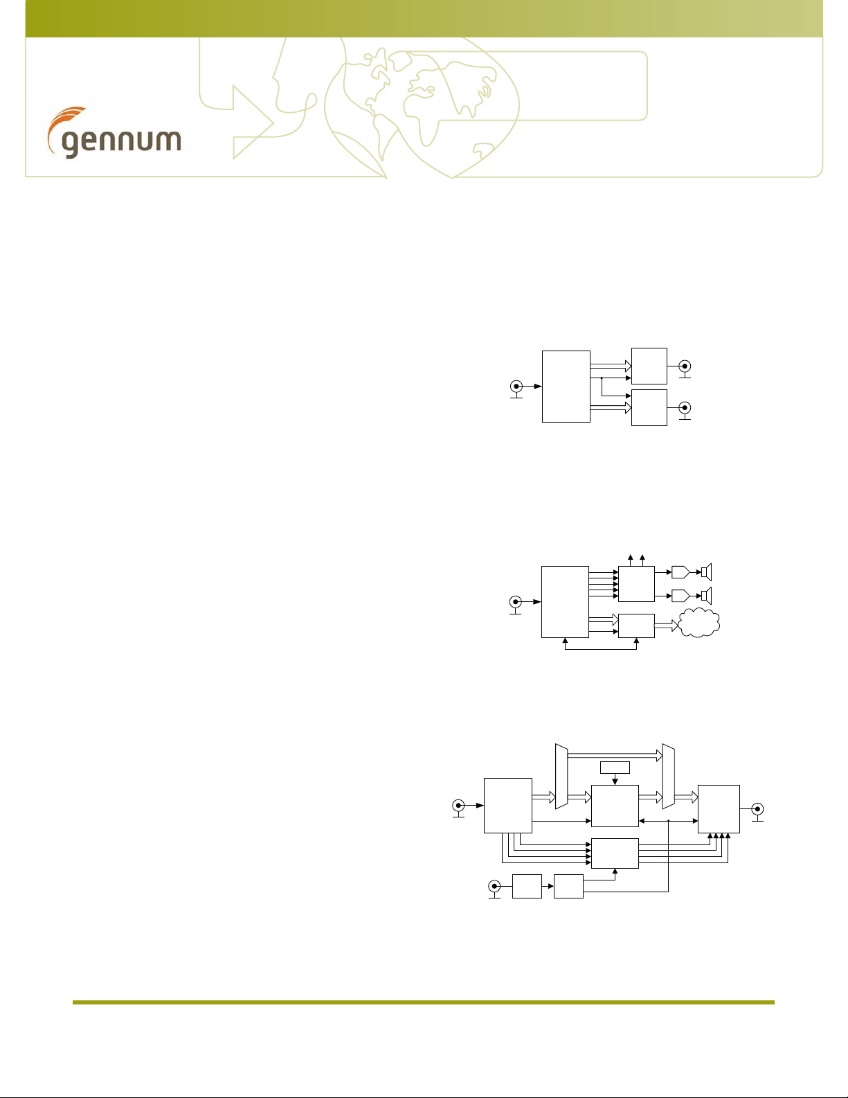
HD-SDI
Application: Single Link (3G-SDI)
to Dual Link (HD-SDI) Converter
GS2962/72
Link A
Link B
HVF/PCLK
10-bit
3G-SDI
GS2971
GS2962/72
10-bit
HVF/PCLK
HD-SDI
Application: 1080p50/60 Monitor
Audio
Selector
Video
Proces sor
10-bit
HVF/PCLK
CTRL/TIMECODE
AES - OUT
AUDIO 1/2
Audio Clocks
Speakers
Display
DAC
DAC
3G-S DI
GS2971
AUDIO 3/4
AUDIO 5/6
AUDIO 7/8
Key Features
• Operation at 2.97Gb/s, 2.97/1.001Gb/s, 1.485Gb/s,
1.485/1.001Gb/s and 270Mb/s
• Supports SMPTE 425M (Level A and Level B), SMPTE
424M, SMPTE 292M, SMPTE 259M-C and DVB-ASI
• Integrated adaptive cable equalizer
• Typical equalized length of Belden 1694A cable:
150m at 2.97Gb/s
250m at 1.485Gb/s
480m at 270Mb/s
• Integrated Reclocker with low phase noise, integrated
VCO
• Serial digital reclocked, or non-reclocked output
• Integrated audio de-embedder for 8 channels of 48kHz
audio
• Integrated audio clock generator
• Ancillary data extraction
• Optional conversion from SMPTE 425M Level B to
Level A for 1080p 50/60 4:2:2 10-bit
• Parallel data bus selectable as either 20-bit or 10-bit
• Comprehensive error detection and correction
features
• Output H, V, F or CEA 861 Timing Signals
• 1.2V digital core power supply, 1.2V and 3.3V analog
power supplies, and selectable 1.8V or 3.3V I/O power
supply
• GSPI Host Interface
• -20ºC to +85ºC operating temperature range
• Low power operation (typically 545mW)
• Small 11mm x 11mm 100-ball BGA package
• Pb-free and ROHS compliant
Applications
Application: Multi-format Downconverter
SD/HS/3G-SDI
Analog
Sync
GS2971
Sync
Seperator
10-bit
HVF/PCLK
AES 1/2
AES 3/4
AES 5/6
AES 7/8
GS4901
10-bit bit SD Bypass
Memory
Video
Downc onverter &
Aspect Ratio
Conversion
Audio
Processing
& Delay
Audio Clocks
HVF/PCLK
AES 1/2
AES 3/4
AES 5/6
AES 7/8
10-bit
HD/SD
Serializer
(GS1582,
GS2972)
SD-SDI
Adaptive Cable Equalizer
Product Brief
51914 - E June 2009
www.gennum.com
1 of 5GS2971 3Gb/s, HD, SD SDI Receiver, with Integrated
Page 2
The device features an Integrated Reclocker with an
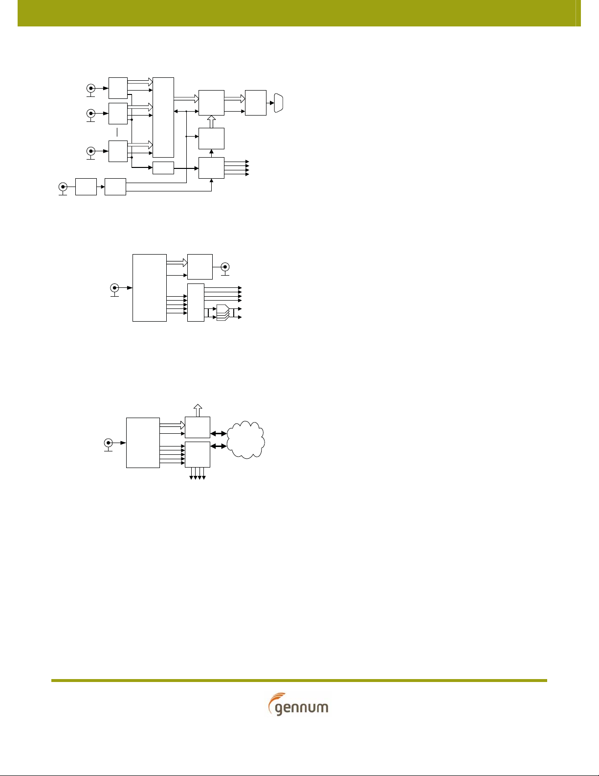
Application: Multi-input Video Monitoring System
GS4911
Analog
Sync
Sync
Seperator
Video
Formatter
Video
Memory
HVF/PCLK
Audio Clocks
10-bit
HVF/PCLK
AES OUT 1/2
AES OUT 3/4
AES OUT 5/6
AES OUT 7/8
HVF/PCLK
HVF/PCLK
Audio
Select
10-bit
10-bit
On Screen
Display
Generator
AES BUS
Audio
Processor
HV/DE/PCLK
DVI/
VGA DAC
Video
Output
3G-SDI
Input 1
GS2971
GS2971
GS2971
3G-SDI
Input 2
3G-SDI
Input n
Application: Multi-format Audio De-embedder Module
PCLK
10- bit
GS2962
DAC
Switch
Logic
&
Drivers
Analog
Audio
Outpu ts
AES
Audio
Outpu ts
AUDIO 1/2
AUDIO 3/4
AUDIO 5/6
AUDIO 7/8
Audio Clocks
SD/HD/3G-SDI
GS2971
SD/HD/3G-SDI
Application: Multi-format Digital VTR/Video Server
Storage :
Tape /HD D/Solid S tate
Audio
Proces sor
Video
Proces sor
10-bit
HVF/PCLK
Audio Outputs
Video Output
Audio Clocks
AUDIO 1/2
AUDIO 3/4
AUDIO 5/6
AUDIO 7/8
SD/HD/3G-SDI
GS2971
internal VCO and a wide Input Jitter Tolerance (IJT) of 0.7UI.
A serial digital loop through output is provided, which can
be configured to output either reclocked or non-reclocked
serial digital data. The Serial Digital Output can be
connected to an external Cable Driver.
The device operates in one of four basic modes: SMPTE
mode, DVB-ASI mode, Data-Through mode or Standby
mode.
In SMPTE mode, the GS2971 performs SMPTE
de-scrambling and NRZI to NRZ decoding and word
alignment. Line-based CRC errors, line number errors, TRS
errors and ancillary data check sum errors can all be
detected. The GS2971 also provides ancillary data
extraction. The entire ancillary data packet is extracted,
and written to host-accessible registers. Other processing
functions include H:V:F timing extraction, Luma and
Chroma ancillary data indication, video standard detection,
and SMPTE 352M packet detection and decoding. All of the
processing features are optional, and may be enabled or
disabled via the Host Interface.
Description
The GS2971 is a multi-rate SDI integrated Receiver which
includes complete SMPTE processing, as per SMPTE 425M,
292M and SMPTE 259M-C. The SMPTE processing features
can be bypassed to support signals with other coding
schemes.
The GS2971 integrates Gennum's next-generation
state-of-the-art adaptive cable equalizer technology,
achieving unprecedented cable lengths and jitter tolerance.
It features DC restoration to compensate for the DC content
of SMPTE pathological signals.
GS2971 3Gb/s, HD, SD SDI Receiver, with Integrated
Adaptive Cable Equalizer
Product Brief
51914 - E June 2009
Both SMPTE 425M Level A and Level B inputs are
supported. The GS2971 also provides user-selectable
conversion from Level B to Level A for 1080p 50/60 4:2:2
10-bit formats only.
In DVB-ASI mode, 8b/10b decoding is applied to the
received data stream.
In Data-Through mode, all forms of SMPTE and DVB-ASI
decoding are disabled, and the device can be used as a
simple serial to parallel converter.
The device can also be placed in a lower power Standby
mode. In this mode, no signal processing is carried out and
the parallel output is held static. Placing the Receiver in
Standby mode will automatically place the integrated
equalizer in power down mode as well.
Parallel data outputs are provided in 20-bit or 10-bit
multiplexed format for 3Gb/s, HD and SD video rates. For
1080p 50/60 4:2:2 10-bit, the parallel data is output on the
20-bit parallel bus as Y on 10 bits and Cb/Cr on the other 10
bits. As such, this parallel bus can interface directly with
video processor ICs. For other SMPTE 425M mapping
structures, the video data is mapped to a 20-bit virtual
interface as described in SMPTE 425M. In all cases this
20-bit parallel bus can be multiplexed onto 10 bits for a low
pin count interface with downstream devices. The
2 of 5
Page 3

associated Parallel Clock input signal operates at 148.5 or
Buffer Mux
Reclocker
with
Integrated
VCO
SDI
SDO
SDO
Serial
to
Parallel
Converter
Descramble,
Word Align,
Rate Detect
Flywheel
Video
Standard
Detect
TRS
Detect
Timing
Extraction
Mux
DVB-ASI
Decoder
Illegal code
remap,
TRS/
Line Number/
CRS
Insertion,
EDH Packet
Insertion
V/VSync
H/HSync
F/De
Rate_det[1:0]
ANC/
Checksum
/352M
Extraction
Audio
De-Embedder,
Audio Clock
Generation
Error Flags
YANC/CANC
LOCKED
DVB_ASI
STANDBY
GSPI and
JTAG Controller
Host
Interface
Output Mux/
Demux
Crystal
Buffer/
Oscillator
LF
LB_CONT
VBG
RC_BYP
I/O Control
TIM861
20BIT/10BIT
SMPTE_BYPASS
IOPROC_EN/DIS
RESET_TRST
CORE_VDD
CORE_GND
IO_VDD
IO_GND
AUDIO_EN/DIS
AOUT_1/2
ACLK
AMCLK
WCLK
CS_TMS
SCLK_TCLK
SDIN_TDI
SDOUT_TDO
JTAG/HOST
XTAL1
SW_EN
VCO_VDD
VCO_GND
PLL_VDD
PLL_GND
EQ_VDD
EQ_GND
A_VDD
A_GND
BUFF_VDD
BUFF_GND
Buffer
SDI
AOUT_3/4
AOUT_5/6
AOUT_7/8
XTAL2
XTAL_OUT
SMPTE 425M
1080p 50/60
4:2:2 10-bit
Level B Level A
NGEN
EQ
AGC+
AGC-
DOUT[19:0]
PCLK
LOCKED
148.5/1.001MHz (for all 3Gb/s HD 10-bit multiplexed
modes), 74.25 or 74.25/1.001MHz (for HD 20-bit mode),
27MHz (for SD 10-bit mode) and 13.5MHz (for SD 20-bit
mode).
Note: for 3Gb/s 10-bit mode the device operates in Dual
Data Rate (DDR) mode, where the data is sampled at both
the rising and falling edges of the clock. This reduces the I/O
speed requirements of the downstream devices.
Up to eight channels, in two groups, of serial digital audio
may be extracted from the video data stream, in accordance
Functional Block Diagram
with SMPTE 272M and SMPTE 299M. The output signal
formats supported by the device include AES/EBU and
three other industry standard serial digital formats. 16, 20
and 24-bit audio formats are supported at 48kHz
synchronous for SD modes and 48kHz synchronous or
asynchronous in HD/3G mode. Additional audio processing
features include group selection, channel swapping, ECC
error detection and correction (HD mode only), and audio
channel status extraction. Audio clock and control signals
provided by the device include Word Clock (fs), Serial Clock
(64fs), and Audio Master Clock at user-selectable rates of
128fs, 256fs or 512fs.
GS2971 Functional Block Diagram
3 of 5
GS2971 3Gb/s, HD, SD SDI Receiver, with Integrated
Product Brief
51914 - E June 2009
Adaptive Cable Equalizer
Page 4

Pin Out
132 45678910
A
B
C
D
E
F
G
H
J
K
PCLK
DVB_ASI
20bit/
10bit
LF
SDO
STANDBY
ACLK
JTAG/
HOST
RESET
_TRST
WCLK
A_VDD
CORE
_GND
SDO
VBG
SDI
SDI
BUFF_
VDD
SDO_
EN/DIS
LB_CONT
VCO_
VDD
VCO_
GND
RSV
PLL_
VDD
A_GND
A_GND
STAT0 STAT1
STAT2 STAT3
STAT4 STAT5
CORE
_GND
CORE
_GND
CORE
_GND
CORE
_VDD
CORE
_VDD
CORE
_VDD
CORE
_VDD
DOUT1
DOUT0 DOUT2 DOUT3
DOUT4 DOUT5
DOUT6 DOUT7
DOUT8 DOUT9
DOUT10 DOUT11
DOUT14 DOUT13
DOUT16 DOUT15
DOUT18 DOUT17
DOUT19
DOUT12
IO_VDD
IO_GND
PLL_
VDD
PLL_
GND
PLL_
VDD
A_GND
A_GND
A_GND
RC_BYP
SW_EN IO_GND IO_VDD
EQ_VDD EQ_GND
PLL_
GND
PLL_
GND
AGC+ RSV
SDOUT_
TDO
CS_
TMS
SDIN_
TDI
SCLK_
TCK
SMPTE_
BYPASS
IO_GND
IO_VDD
AUDIO_
EN/DIS
AMCLK
AOUT
_1/2
AOUT
_3/4
AOUT
_5/6
AOUT
_7/8
TIM_861
XTAL_
OUT
XTAL2
XTAL1
IO_GND
IO_VDD
IOPROC_
EN/DIS
AGC- A_GND
BUFF_
GND
CORE
_GND
GS2971 Pin Out
The following table shows the pin difference between the GS2970 and the GS2971:
Pin Number GS2970 GS2971 Functional Description of the GS2971 Pins
E1 SDI_VDD EQ_VDD POWER pin for the EQ.
E2 SDI_GND EQ_GND GND pin for the EQ.
F1 TERM AGC+ Attach the AGC capacitor between this pin and AGC-.
G1RSVAGC- Attach the AGC capacitor between this pin and AGC+.
G2RSVA_GND Analog GND pin.
G4RSV CORE_GND GND connection – digital logic.
GS2971 3Gb/s, HD, SD SDI Receiver, with Integrated
Adaptive Cable Equalizer
Product Brief
51914 - E June 2009
4 of 5
Page 5

DOCUMENT IDENTIFICATION
PRODUCT BRIEF
The product is in a development phase and specifications are subject to change
without notice. Gennum reserves the right to remove the product at any time.
Listing the product does not constitute an offer for sale.
CAUTION
ELECTROSTATIC SENSITIVE DEVICES
DO NOT OPEN PACKAGES OR HANDLE EXCEPT AT A
STATIC-FREE WORKSTAT IO N
GENNUM CORPORATE HEADQUARTERS
4281 Harvester Road, Burlington, Ontario L7L 5M4 Canada
OTTAWA
232 Herzberg Road, Suite 101
Kanata, Ontario K2K 2A1
Canada
Phone: +1 (613) 270-0458
Fax: +1 (613) 270-0429
CALGARY
3553 - 31st St. N.W., Suite 210
Calgary, Alberta T2L 2K7
Canada
Phone: +1 (403) 284-2672
UNITED KINGDOM
North Building, Walden Court
Parsonage Lane,
Bishop’s Stortford Hertfordshire, CM23 5DB
United Kingdom
Phone: +44 1279 714170
Fax: +44 1279 714171
INDIA
#208(A), Nirmala Plaza,
Airport Road, Forest Park Square
Bhubaneswar 751009
India
Phone: +91 (674) 653-4815
Fax: +91 (674) 259-5733
SNOWBUSH IP - A DIVISION OF GENNUM
439 University Ave. Suite 1700
Toronto, Ontario M5G 1Y8
Canada
Phone: +1 (416) 925-5643
Fax: +1 (416) 925-0581
E-mail: sales@snowbush.com
Web Site: http://www.snowbush.com
MEXICO
288-A Paseo de Maravillas
Jesus Ma., Aguascalientes
Mexico 20900
Phone: +1 (416) 848-0328
JAPAN KK
Shinjuku Green Tower Building 27F
6-14-1, Nishi Shinjuku
Shinjuku-ku, Tokyo, 160-0023
Japan
Phone: +81 (03) 3349-5501
Fax: +81 (03) 3349-5505
E-mail: gennum-japan@gennum.com
Web Site: http://www.gennum.co.jp
TA IW A N
6F-4, No.51, Sec.2, Keelung Rd.
Sinyi District, Taipei City 11502
Taiwan R.O.C.
Phone: (886) 2-8732-8879
Fax: (886) 2-8732-8870
E-mail: gennum-taiwan@gennum.com
Phone: +1 (905) 632-2996 Fax: +1 (905) 632-2055
E-mail: corporate@gennum.com www.gennum.com
GERMANY
Hainbuchenstraße 2
80935 Muenchen (Munich), Germany
Phone: +49-89-35831696
Fax: +49-89-35804653
E-mail: gennum-germany@gennum.com
NORTH AMERICA WESTERN REGION
Bayshore Plaza
2107 N 1st Street, Suite #300
San Jose, CA 95131
United States
Phone: +1 (408) 392-9454
Fax: +1 (408) 392-9427
E-mail: naw_sales@gennum.com
NORTH AMERICA EASTERN REGION
4281 Harvester Road
Burlington, Ontario L7L 5M4
Canada
Phone: +1 (905) 632-2996
Fax: +1 (905) 632-2055
E-mail: nae_sales@gennum.com
KOREA
8F Jinnex Lakeview Bldg.
65-2, Bangidong, Songpagu
Seoul, Korea 138-828
Phone: +82-2-414-2991
Fax: +82-2-414-2998
E-mail: gennum-korea@gennum.com
Gennum Corporation assumes no liability for any errors or omissions in this document, or for the use of the circuits or devices described herein. The sale of
the circuit or device described herein does not imply any patent license, and Gennum makes no representation that the circuit or device is free from patent
infringement.
All other trademarks mentioned are the properties of their respective owners.
GENNUM and the Gennum logo are registered trademarks of Gennum Corporation.
© Copyright 2009 Gennum Corporation. All rights reserved.
gennum.com
www.
GS2971 3Gb/s, HD, SD SDI Receiver, with Integrated
Adaptive Cable Equalizer
5
5 of 5
Product Brief
51914 - E June 2009
 Loading...