

Page 1

GS1531 HD-LINX® II
Multi-Rate Serializer with ClockCleaner™
GS1531 Data Sheet
Key Features
• SMPTE 292M and SMPTE 259M-C compliant
scrambling and NRZ → NRZI encoding (with
bypass)
• DVB-ASI sync word insertion and 8b/10b encoding
• Rejection of more than 300ps jitter on the input
PCLK
• User selectable additional processing features
including:
• CRC, ANC data checksum, and line number
calculation and insertion
• TRS and EDH packet generation and insertion
• illegal code remapping
• Internal flywheel for noise immune TRS generation
• 20-bit / 10-bit CMOS parallel input data bus
• 148.5MHz / 74.25MHz / 27MHz / 13.5MHz parallel
digital input
• Automatic standards detection and indication
• 1.8V core power supply and 3.3V charge pump
power supply
• 3.3V digital I/O supply
• JTAG test interface
• Available in a Pb-free package
• small footprint (11mm x 11mm)
Applications
• SMPTE 292M Serial Digital Interfaces
• SMPTE 259M-C Serial Digital Interfaces
• DVB-ASI Serial Digital Interfaces
Description
The GS1531 is a multi-standard serializer with an
integrated cable driver. When used in conjunction with
the GO1555/GO1525* Voltage Controlled Oscillator, a
transmit solution can be realized for HD-SDI, SD-SDI
and DVB-ASI applications.
The device features an internal PLL, which can be
configured for loop bandwidth as narrow as 100kHz.
Thus the GS1531 can tolerate in excess of 300ps jitter
on the input PCLK and still provide output jitter well
within SMPTE specification. Connect the output clocks
from Gennum’s GS4911 clock generator directly to the
GS1531’s PCLK input and configure the GS1531’s loop
bandwidth accordingly.
In addition to serializing the input, the GS1531 performs
NRZ-to-NRZI encoding and scrambling as per SMPTE
292M/259M-C when operating in SMPTE mode. When
operating in DVB-ASI mode, the device will insert K28.5
sync characters and 8b/10b encode the data prior to
serialization.
Parallel data inputs are provided for 10-bit multiplexed
or 20-bit demultiplexed formats at both HD and SD
signal rates. An appropriate parallel clock input signal is
also required.
The integrated cable driver features an output mute on
loss of parallel clock, high impedance mode, adjustable
signal swing, and automatic dual slew rate selection
depending on HD/SD operational requirements.
The GS1531 also includes a range of data processing
functions including automatic standards detection and
EDH support. The device can also insert TRS signals,
calculate and insert line numbers and CRC’s, re-map
illegal code words and insert SMPTE 352M payload
identifier packets. All processing features are optional
and may be enabled/disabled via external control pin(s)
and/or host interface programming.
*For new designs use GO1555
30573 - 7 February 2008 1 of 50
www.gennum.com
Page 2
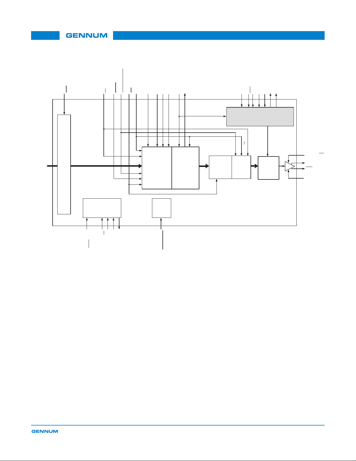
Functional Block Diagram
SDO
SDO
SDO_EN/DIS
RSET
CP_CAP
H
V
F
DIN[19:0]
IOPROC_EN/DIS
DVB_ASI
I/O
Buffer
&
demux
SMPTE
352M
generation
TRS insertion,
Line number
insertion,
CRC insertion,
data blank, code re-map and
flywheel
dvb-asi
bypass
RESET_TRST
Reset
HOST Interface /
JTAG test
CS_TMS
SCLK_TCK
SDIN_TDI
SDOUT_TDO
JTAG/HOST
LOCKED
V
CO
VCO
LF
LB_CONT
VCO_VCC
VCO_GND
SD/HD
20bit/10bit
DVB-ASI sync
word insert &
8b/10b encode
EDH
generation
& SMPTE
scramble
PCLK
BLANK
DETECT_TRS
SMPTE_BYPASS
Phase detector, charge pump,
VCO control & power supply
P -> S
sd/hd
ClockCleaner™
GS1531 Data Sheet
GS1531 Functional Block Diagram
30573 - 7 February 2008 2 of 50
Page 3

GS1531 Data Sheet
Contents
Key Features.................................................................................................................1
Applications...................................................................................................................1
Description ....................................................................................................................1
Functional Block Diagram .............................................................................................2
1. Pin Out .....................................................................................................................5
1.1 Pin Assignment ...............................................................................................5
1.2 Pin Descriptions ..............................................................................................6
2. Electrical Characteristics........................................................................................13
2.1 Absolute Maximum Ratings ..........................................................................13
2.2 DC Electrical Characteristics ........................................................................13
2.3 AC Electrical Characteristics.........................................................................14
2.4 Solder Reflow Profiles...................................................................................16
3. Input/Output Circuits ..............................................................................................17
3.1 Host Interface Maps......................................................................................19
3.1.1 Host Interface Map (Read Only Registers).........................................20
3.1.2 Host Interface Map (R/W Configurable Registers) .............................21
4. Detailed Description ...............................................................................................22
4.1 Functional Overview .....................................................................................22
4.2 Parallel Data Inputs.......................................................................................22
4.2.1 Parallel Input in SMPTE Mode............................................................23
4.2.2 Parallel Input in DVB-ASI Mode..........................................................23
4.2.3 Parallel Input in Data-Through Mode ..................................................23
4.2.4 Parallel Input Clock (PCLK) ................................................................24
4.3 SMPTE Mode................................................................................................25
4.3.1 Internal Flywheel.................................................................................25
4.3.2 HVF Timing Signal Extraction.............................................................25
4.4 DVB-ASI mode..............................................................................................26
4.4.1 Control Signal Inputs ..........................................................................27
4.5 Data-Through Mode......................................................................................28
4.6 Additional Processing Functions...................................................................28
4.6.1 Input Data Blank .................................................................................28
4.6.2 Automatic Video Standard Detection..................................................28
4.6.3 Packet Generation and Insertion ........................................................30
4.7 Parallel-To-Serial Conversion .......................................................................37
4.8 Serial Digital Data PLL..................................................................................38
4.8.1 External VCO......................................................................................38
4.8.2 Lock Detect Output .............................................................................38
4.8.3 Loop Bandwidth Adjustment ...............................................................39
4.9 Serial Digital Output ......................................................................................39
4.9.1 Output Swing ......................................................................................39
30573 - 7 February 2008 3 of 50
Page 4

GS1531 Data Sheet
4.9.2 Serial Digital Output Mute...................................................................40
4.10 GSPI Host Interface ....................................................................................40
4.10.1 Command Word Description.............................................................41
4.10.2 Data Read and Write Timing ............................................................42
4.10.3 Configuration and Status Registers ..................................................43
4.11 JTAG...........................................................................................................43
4.12 Device Power Up ........................................................................................45
4.13 Device Reset...............................................................................................45
5. Application Reference Design................................................................................46
5.1 Typical Application Circuit.............................................................................46
6. References & Relevant Standards.........................................................................47
7. Package & Ordering Information............................................................................48
7.1 Package Dimensions ....................................................................................48
7.2 Packaging Data.............................................................................................49
7.3 Ordering Information .....................................................................................49
8. Revision History .....................................................................................................50
30573 - 7 February 2008 4 of 50
Page 5
1. Pin Out
1
32
45
6
7
8
9
10
A
B
C
D
E
F
G
H
J
K
LOCKED
PCLK
LB_
CONT
NC
DIN19
DIN18
DIN17
DIN16
DIN14
DIN12
DIN10
DIN8
DIN6
DIN4
DIN2
DIN1
DIN15
DIN13
DIN11
DIN9
DIN7
DIN5
DIN3
DIN0
SD/HD
IO_VDD
IO_VDD
IO_GND
BLANK
H
IO_VDD
CORE
_VDD
IO_GND
CORE
_VDD
CORE
_GND
CORE
_GND
DETECT
_TRS
DVB_ASI
SMPTE_
BYPASS
NC
NC
20bit/
10bit
SDIN
_TDI
SCLK
_TCK
SDOUT
_TDO
CS_
TMS
NC
NC
NC
CD_VDD
RSET
NC
NC
NC
NC
NC
NC
NC
NC
NC
CP_CAP
SDO
SD0
VCO_
VCC
VCO_
GND
LF
VCO
VCO
CP_VDD
CP_GND
PD_VDD
PD_GND
NC
NC
NC
NC
V
IO_GND
CD_GND
F
NCNC
NC
NC
NC
NC
NC
NC
NC
NC
RSV
NC
NC
NC
NC
NC
JTAG/
HOST
SDO_EN
/DIS
RESET
_TRST
IOPROC
_EN/DIS
1.1 Pin Assignment
GS1531 Data Sheet
30573 - 7 February 2008 5 of 50
Page 6
1.2 Pin Descriptions
Table 1-1: Pin Descriptions
GS1531 Data Sheet
Pin
Name Timing Type Description
Number
A1 LF Analog Output Control voltage to external voltage controlled oscillator. Nominally +1.25V
A2 VCO_VCC – Output
Power
A3 VCO_GND – Output
Power
A4, A5 VCO
A6, B5,
B6, C1,
C4, C5,
C6, C7,
C8, D1,
D2, D3,
D4, D7,
D8, E1,
E2, E3,
E7, F2,
F3, F7,
G1, G2,
G3, G7,
H1, H2,
H3, H7,
J1, J2,
J3, J4
, VCO Analog Input Differential inputs for the external VCO reference signal. For single ended
NC – – No connect.
DC.
Power supply for the external voltage controlled oscillator. Connect to pin
7 of the GO1555/GO1525*. This pin is an output.
Should be isolated from all other power supplies.
*For new designs use GO1555
Ground reference for the external voltage controlled oscillator. Connect to
pins 2, 4, 6, and 8 of the GO1555/GO1525*. This pin is an output.
Should be isolated from all other grounds.
*For new designs use GO1555
devices such as the GO1555/GO1525*, VCO
VCO_GND.
VCO is nominally 1.485GHz.
*For new designs use GO1555
should be AC coupled to
A7 PCLK – Input PARALLEL DATA BUS CLOCK
Signal levels are LVCMOS/LVTTL compatible.
HD 20-bit mode PCLK = 74.25MHz or 74.25/1.001MHz
HD 10-bit mode PCLK = 148.5MHz or 148.5/1.001MHz
SD 20-bit mode PCLK = 13.5MHz
SD 10-bit mode PCLK = 27MHz
A8, E8, K8 IO_VDD – Power Power supply connection for digital I/O buffers. Connect to +3.3V DC
30573 - 7 February 2008 6 of 50
digital.
Page 7
Table 1-1: Pin Descriptions (Continued)
GS1531 Data Sheet
Pin
Number
A10, A9,
B10, B9,
C10, C9,
D10, D9,
E10, E9
Name Timing Type Description
DIN[19:10] Synchronous
with PCLK
Input PARALLEL DATA BUS
Signal levels are LVCMOS/LVTTL compatible.
DIN19 is the MSB and DIN10 is the LSB.
HD 20-bit mode
SD/HD
= LOW
20bit/10bit
HD 10-bit mode
SD/HD
= LOW
20bit/10bit
SD 20-bit mode
SD/HD
= HIGH
20bit/10bit
= HIGH
= LOW
= HIGH
Luma data input in SMPTE mode
SMPTE_BYPASS
DVB_ASI = LOW
Data input in Data-Through mode
SMPTE_BYPASS
DVB_ASI = LOW
Multiplexed Luma and Chroma data input
in SMPTE mode
SMPTE_BYPASS
DVB_ASI = LOW
Data input in Data-Through mode
SMPTE_BYPASS
DVB_ASI = LOW
Luma data input in SMPTE mode
SMPTE_BYPASS
DVB_ASI = LOW
Data input in Data-Through mode
SMPTE_BYPASS
DVB_ASI = LOW
DVB-ASI data input in DVB-ASI mode
SMPTE_BYPASS
DVB_ASI = HIGH
= HIGH
= LOW
= HIGH
= LOW
= HIGH
= LOW
= LOW
SD 10-bit mode
SD/HD
= HIGH
20bit/10bit
B1 CP_CAP Analog Input PLL lock time constant capacitor connection.
B2 CP_VDD – Power Power supply connection for the charge pump. Connect to +3.3V DC
B3 CP_GND – Power Ground connection for the charge pump. Connect to analog GND.
B4 LB_CONT Analog Input Control voltage to set the loop bandwidth of the integrated reclocker.
B7 DETECT_TRS Non
Synchronous
Input CONTROL SIGNAL INPUT
analog.
Signal levels are LVCMOS/LVTTL compatible.
Used to select the timing mode of the device.
When set HIGH, the device will lock the internal flywheel to the embedded
TRS timing signals in the parallel input data.
When set LOW, the device will lock the internal flywheel to the externally
supplied H, V, and F input signals.
= LOW
Multiplexed Luma and Chroma data input
in SMPTE mode
SMPTE_BYPASS
DVB_ASI = LOW
Data input in data through mode
SMPTE_BYPASS
DVB_ASI = LOW
DVB-ASI data input in DVB-ASI mode
SMPTE_BYPASS
DVB_ASI = HIGH
= HIGH
= LOW
= LOW
30573 - 7 February 2008 7 of 50
Page 8
Table 1-1: Pin Descriptions (Continued)
GS1531 Data Sheet
Pin
Name Timing Type Description
Number
B8, F8, J8 IO_GND – Power Ground connection for digital I/O buffers. Connect to digital GND.
C2 PD_VDD – Power Power supply connection for the phase detector. Connect to +1.8V DC
analog.
C3 PD_GND – Power Ground connection for the phase detector. Connect to analog GND.
D5 DVB_ASI Non
Synchronous
D6 LOCKED Synchronous
with PCLK
E4 SD/HD
Non
Synchronous
Input CONTROL SIGNAL INPUT
Signal levels are LVCMOS/LVTTL compatible.
When set HIGH in conjunction with SD/HD
= LOW, the device will be configured to operate in DVB-ASI mode.
When set LOW, the device will not support the encoding of received
DVB-ASI data.
Output STATUS SIGNAL OUTPUT
Signal levels are LVCMOS / LVTTL compatible.
The LOCKED signal will be HIGH whenever the device has correctly
received and locked to SMPTE compliant data in SMPTE mode or
DVB-ASI compliant data in DVB-ASI mode, or when the device has
achieved lock in Data-Through mode.
It will be LOW otherwise.
Input CONTROL SIGNAL INPUT
Signal levels are LVCMOS/LVTTL compatible.
When set LOW, the device will be configured to transmit signal rates of
1.485Gb/s or 1.485/1.001Gb/s only.
When set HIGH, the device will be configured to transmit signal rates of
270Mb/s only.
= HIGH and SMPTE_BYPASS
E5, F5 CORE_GND – Power Ground connection for the digital core logic. Connect to digital GND.
E6, F6 CORE_VDD – Power Power supply connection for the digital core logic. Connect to +1.8V DC
digital.
F1 RSV – – Connect to Analog GND.
F4 20bit/10bit
Non
Synchronous
Input CONTROL SIGNAL INPUT
Signal levels are LVCMOS/LVTTL compatible.
Used to select the input data bus width in SMPTE or Data-Through
modes.
When set HIGH, the parallel input will be 20-bit demultiplexed data.
When set LOW, the parallel input will be 10-bit multiplexed data.
30573 - 7 February 2008 8 of 50
Page 9
Table 1-1: Pin Descriptions (Continued)
GS1531 Data Sheet
Pin
Number
F10, F9,
G10, G9,
H10, H9,
J10, J9,
K10, K9
Name Timing Type Description
DIN[9:0] Synchronous
with PCLK
Input PARALLEL DATA BUS
Signal levels are LVCMOS/LVTTL compatible.
DIN9 is the MSB and DIN0 is the LSB.
HD 20-bit mode
SD/HD
= LOW
20bit/10bit
HD 10-bit mode
SD/HD
20bit/10bit
SD 20-bit mode
SD/HD
20bit/10bit
SD 10-bit mode
SD/HD
20bit/10bit
= HIGH
= LOW
= LOW
= HIGH
= HIGH
= HIGH
= LOW
Chroma data input in SMPTE mode
SMPTE_BYPASS
DVB_ASI = LOW
Data input in Data-Through mode
SMPTE_BYPASS
DVB_ASI = LOW
High impedance in all modes.
Chroma data input in SMPTE mode
SMPTE_BYPASS
DVB_ASI = LOW
Data input in Data-Through mode
SMPTE_BYPASS
DVB_ASI = LOW
High impedance in DVB-ASI mode
SMPTE_BYPASS
DVB_ASI = HIGH
High impedance in all modes.
=HIGH
= LOW
= HIGH
= LOW
= LOW
G4 IOPROC_EN/DIS
Non
Synchronous
Input CONTROL SIGNAL INPUT
Signal levels are LVCMOS/LVTTL compatible.
Used to enable or disable I/O processing features.
When set HIGH, the following I/O processing features of the device are
enabled:
• EDH Packet Generation and Insertion (SD-only)
• SMPTE 352M Packet Generation and Insertion
• ANC Data Checksum Calculation and Insertion
• Line-based CRC Generation and Insertion (HD-only)
• Line Number Generation and Insertion (HD-only)
• TRS Generation and Insertion
• Illegal Code Remapping
To enable a subset of these features, keep IOPROC_EN/DIS
disable the individual feature(s) in the IOPROC_DISABLE register
accessible via the host interface.
When set LOW, the I/O processing features of the device are disabled,
regardless of whether the features are enabled in the IOPROC_DISABLE
register.
HIGH and
30573 - 7 February 2008 9 of 50
Page 10
Table 1-1: Pin Descriptions (Continued)
GS1531 Data Sheet
Pin
Name Timing Type Description
Number
G5 SMPTE_BYPASS
G6 RESET_TRST
G8 BLANK
Non
Synchronous
Non
Synchronous
Synchronous
with PCLK
Input CONTROL SIGNAL INPUT
Signal levels are LVCMOS/LVTTL compatible.
When set HIGH in conjunction with DVB_ASI = LOW, the device will be
configured to operate in SMPTE mode. All I/O processing features may be
enabled in this mode.
When set LOW, the device will not support the scrambling or encoding of
received SMPTE data. No I/O processing features will be available.
Input CONTROL SIGNAL INPUT
Signal levels are LVCMOS/LVTTL compatible.
Used to reset the internal operating conditions to default settings and to
reset the JTAG test sequence.
Host Mode (JTAG/HOST
When asserted LOW, all functional blocks will be set to default conditions
and all input and output signals become high
serial digital outputs SDO and
Must be set HIGH for normal device operation.
JTAG Test Mode (JTAG/HOST
When asserted LOW, all functional blocks will be set to default and the
JTAG test sequence will be held in reset.
When set HIGH, normal operation of the JTAG test sequence resumes.
Input CONTROL SIGNAL INPUT
Signal levels are LVCMOS/LVTTL compatible.
Used to enable or disable input data blanking.
When set LOW, the luma and chroma input data is set to the appropriate
blanking levels. Horizontal and vertical ancillary spaces will also be set to
blanking levels.
When set HIGH, the luma and chroma input data pass through the device
unaltered.
= LOW)
impedance, including the
SDO.
= HIGH)
H4 CS
H5 SCLK_TCK Non
_TMS Synchronous
with
SCLK_TCK
Synchronous
30573 - 7 February 2008 10 of 50
Input CONTROL SIGNAL INPUT
Signal levels are LVCMOS/LVTTL compatible.
Chip Select / Test Mode Select
Host Mode (JTAG/HOST
CS
_TMS operates as the host interface chip select, CS, and is active
LOW.
JTAG Test Mode (JTAG/HOST
CS
_TMS operates as the JTAG test mode select, TMS, and is active
HIGH.
NOTE: If the host interface is not being used, tie this pin HIGH.
Input CONTROL SIGNAL INPUT
Signal levels are LVCMOS/LVTTL compatible.
Serial Data Clock / Test Clock.
Host Mode (JTAG/HOST
SCLK_TCK operates as the host interface burst clock, SCLK. Command
and data read/write words are clocked into the device synchronously with
this clock.
JTAG Test Mode (JTAG/HOST
SCLK_TCK operates as the JTAG test clock, TCK.
NOTE: If the host interface is not being used, tie this pin HIGH.
= LOW)
= LOW)
= HIGH)
= HIGH)
Page 11

Table 1-1: Pin Descriptions (Continued)
GS1531 Data Sheet
Pin
Name Timing Type Description
Number
H6 SDOUT_TDO Synchronous
SCLK_TCK
H8 H Synchronous
with PCLK
with
Output CONTROL SIGNAL OUTPUT
Signal levels are LVCMOS/LVTTL compatible.
Serial Data Output / Test Data Output
Host Mode (JTAG/HOST
SDOUT_TDO operates as the host interface serial output, SDOUT, used
to read status and configuration information from the internal registers of
the device.
JTAG Test Mode (JTAG/HOST
SDOUT_TDO operates as the JTAG test data output, TDO.
Input CONTROL SIGNAL INPUT
Signal levels are LVCMOS/LVTTL compatible.
Used to indicate the portion of the video line containing active video data
when DETECT_TRS is set LOW. The device will set the H bit in all
outgoing TRS signals for the entire period that the H input signal is HIGH
(IOPROC_EN/DIS
H signal timing is configurable via the H_CONFIG bit of the
IOPROC_DISABLE register, accessible via the host interface.
Active Line Blanking (H_CONFIG = 0
The H signal should be set HIGH for the entire horizontal blanking period,
including the EAV and SAV TRS words, and LOW otherwise. This is the
default setting.
TRS Based Blanking (H_CONFIG = 1
The H signal should be set HIGH for the entire horizontal blanking period
as indicated by the H bit in the received TRS ID words, and LOW
otherwise.
= LOW)
must also be HIGH).
= HIGH)
h
)
)
h
J5 SDO_EN/DIS
J6 SDIN_TDI Synchronous
Non
Synchronous
with
SCLK_TCK
Input CONTROL SIGNAL INPUT
Input CONTROL SIGNAL INPUT
Signal levels are LVCMOS/LVTTL compatible.
Used to enable or disable the serial digital output stage.
When set LOW, the serial digital output signals SDO and SDO
disabled and become high impedance.
When set HIGH, the serial digital output signals SDO and SDO
enabled.
Signal levels are LVCMOS/LVTTL compatible.
Serial Data In / Test Data Input
Host Mode (JTAG/HOST
SDIN_TDI operates as the host interface serial input, SDIN, used to write
address and configuration information to the internal registers of the
device.
JTAG Test Mode (JTAG/HOST
SDIN_TDI operates as the JTAG test data input, TDI.
NOTE: If the host interface is not being used, tie this pin HIGH.
= LOW)
are
are
= HIGH)
30573 - 7 February 2008 11 of 50
Page 12
Table 1-1: Pin Descriptions (Continued)
GS1531 Data Sheet
Pin
Name Timing Type Description
Number
J7 V Synchronous
with PCLK
K1 RSET Analog Input Used to set the serial digital output signal amplitude. Connect to CD_VDD
K2 CD_VDD – Power Power supply connection for the serial digital cable driver. Connect to
K3, K4 SDO, SDO
K5 CD_GND – Power Ground connection for the serial digital cable driver. Connect to analog
K6 JTAG/HOST
Analog Output Serial digital output signal operating at 1.485Gb/s, 1.485/1.001Gb/s, or
Non
Synchronous
Input CONTROL SIGNAL INPUT
Signal levels are LVCMOS/LVTTL compatible.
Used to indicate the portion of the video field / frame that is used for
vertical blanking when DETECT_TRS is set LOW. The device will set the
V bit in all outgoing TRS signals for the entire period that the V input signal
is HIGH (IOPROC_EN/DIS
The V signal should be set HIGH for the entire vertical blanking period and
should be set LOW for all lines outside of the vertical blanking interval.
The V signal is ignored when DETECT_TRS = HIGH.
through 281Ω +/- 1% for 800mV
+1.8V DC analog.
270Mb/s.
The slew rate of these outputs is automatically controlled to meet SMPTE
292M and 259M requirements according to the setting of the SD/HD
GND.
Input CONTROL SIGNAL INPUT
Signal levels are LVCMOS/LVTTL compatible.
Used to select JTAG Test Mode or Host Interface Mode.
When set HIGH, CS
configured for JTAG boundary scan testing.
When set LOW, CS
configured as GSPI pins for normal host interface operation.
_TMS, SDOUT_TDO, SDI_TDI and SCLK_TCK are
_TMS, SDOUT_TDO, SDI_TDI and SCLK_TCK are
must also be HIGH).
single-ended output swing.
p-p
pin.
K7 F Synchronous
with PCLK
30573 - 7 February 2008 12 of 50
Input CONTROL SIGNAL INPUT
Signal levels are LVCMOS/LVTTL compatible.
Used to indicate the ODD / EVEN field of the video signal when
DETECT_TRS is set LOW. The device will set the F bit in all outgoing TRS
signals for the entire period that the F input signal is HIGH
(IOPROC_EN/DIS
The F signal should be set HIGH for the entire period of field 2 and should
be set LOW for all lines in field 1 and for all lines in progressive scan
systems.
The F signal is ignored when DETECT_TRS = HIGH.
must also be HIGH).
Page 13
2. Electrical Characteristics
2.1 Absolute Maximum Ratings
Parameter Value/Units
Supply Voltage Core -0.3V to +2.1V
Supply Voltage I/O -0.3V to +4.6V
Input Voltage Range (any input) -2.0V to + 5.25V
GS1531 Data Sheet
Ambient Operating Temperature -20°C <
Storage Temperature -40°C <
ESD Protection On All Pins (see Note 1) 1kV
NOTES:
1. HBM, per JESDA-114B.
TA < 85°C
T
< 125°C
STG
2.2 DC Electrical Characteristics
Table 2-1: DC Electrical Characteristics
TA = 0°C to 70°C, unless otherwise specified.
Parameter Symbol Conditions Min Typ Max Units Test
Level
System
Operation Temperature Range T
Digital Core Supply Voltage CORE_VDD – 1.71 1.8 1.89 V 3 1
Digital I/O Supply Voltage IO_VDD – 3.13 3.3 3.47 V 3 1
Charge Pump Supply Voltage CP_VDD – 3.13 3.3 3.47 V 3 1
Phase Detector Supply Voltage PD_VDD – 1.71 1.8 1.89 V 3 1
Input Buffer Supply Voltage BUFF_VDD – 1.71 1.8 1.89 V 3 1
Cable Driver Supply Voltage CD_VDD – 1.71 1.8 1.89 V 3 1
External VCO Supply Voltage
Output
+1.8V Supply Current I
+3.3V Supply Current I
To t a l Dev i c e P o we r P
A
VCO_VCC – 2.25 – 2.75 V 1 –
1V8
3V3
D
–0–70°C31
SDO Enabled – – 245 mA 3 3
–––45mA34
SDO Enabled – – 590 mW 3 –
Notes
30573 - 7 February 2008 13 of 50
Page 14
Table 2-1: DC Electrical Characteristics (Continued)
TA = 0°C to 70°C, unless otherwise specified.
GS1531 Data Sheet
Parameter Symbol Conditions Min Typ Max Units Test
Level
Digital I/O
Input Logic LOW V
Input Logic HIGH V
Output Logic LOW V
Output Logic HIGH V
IL
IH
OL
OH
––– 0.8V4–
–2.1––V4–
+8mA – 0.2 0.4 V 4 –
-8mA IO_VDD - 0.4 – – V 4 –
Input
RSET Voltage V
RSET
RSET=281Ω 0.54 0.6 0.66 V 1 2
Output
Output Common Mode Voltage V
TEST LEVELS
1. Production test at room temperature and nominal supply
voltage with guardbands for supply and temperature ranges.
2. Production test at room temperature and nominal supply
voltage with guardbands for supply and temperature ranges
using correlated test.
3. Production test at room temperature and nominal supply
voltage.
4. QA sample test.
5. Calculated result based on Level 1, 2, or 3.
6. Not tested. Guaranteed by design simulations.
7. Not tested. Based on characterization of nominal parts.
8. Not tested. Based on existing design/characterization data of
similar product.
9. Indirect test.
CMOUT
75Ω load,
RSET=281Ω,
SD and HD
0.8 1.0 1.2 V 1 –
NOTES
1. All DC and AC electrical parameters within specification.
2. Set by the value of the RSET resistor.
3. Sum of all 1.8V supplies.
4. Sum of all 3.3V supplies.
Notes
2.3 AC Electrical Characteristics
Table 2-2: AC Electrical Characteristics
TA = 0°C to 70°C, unless otherwise shown
Parameter Symbol Conditions Min Typ Max Units Test
Level
System
Device Latency – 10-bit SD – 21 – PCLK 8 –
– 20-bit HD – 19 – PCLK 8 –
– DVB-ASI – 11 – PCLK 8 –
Reset Pulse Width t
reset
–1––ms81
30573 - 7 February 2008 14 of 50
Notes
Page 15
Table 2-2: AC Electrical Characteristics (Continued)
TA = 0°C to 70°C, unless otherwise shown
GS1531 Data Sheet
Parameter Symbol Conditions Min Typ Max Units Test
Notes
Level
Parallel Input
Parallel Clock Frequency f
PCLK
Parallel Clock Duty Cycle DC
Input Data Setup Time t
Input Data Hold Time t
su
ih
PCLK
– 13.5 – 148.5 MHz 4 –
–40– 60%6–
–2.0––ns5–
–1.5––ns5–
Serial Digital Output
Serial Output Data Rate DR
Serial Output Swing ΔV
Serial Output Rise Time
20% ~ 80%
Serial Output Fall Time
20% ~ 80%
Serial Output Intrinsic Jitter t
tr
tr
tf
tf
IJ
t
IJ
SDO
SDD
SDO
SDO
SDO
SDO
– – 1.485 – Gb/s 1 –
– – 1.485/1.001 – Gb/s 9 –
– –270–Mb/s1–
RSET = 281Ω
650 800 950 mVp-p 1 –
75Ω load
HD signal – – 260 ps 1 –
SD signal 400 550 1500 ps 1 –
HD signal – – 260 ps 1 –
SD signal 400 550 1500 ps 1 –
Pseudorandom and
–90125ps5–
pathological HD signal
Pseudorandom and
–270350ps5 –
pathological SD signal
GSPI
GSPI Input Clock Frequency f
GSPI Input Clock Duty Cycle DC
SCLK
SCLK
GSPI Input Data Setup Time – – 0 – – ns 8 –
GSPI Input Data Hold Time – – 1.43 – – ns 8 –
GSPI Output Data Hold Time – – 2.1 – – ns 8 –
GSPI Output Data Delay
– – – – 7.27 ns 8 –
Time
TEST LEVELS
1. Production test at room temperature and nominal supply voltage
with guardbands for supply and temperature ranges.
2. Production test at room temperature and nominal supply voltage
with guardbands for supply and temperature ranges using
correlated test.
3. Production test at room temperature and nominal supply voltage.
4. QA sample test.
5. Calculated result based on Level 1, 2, or 3.
6. Not tested. Guaranteed by design simulations.
7. Not tested. Based on characterization of nominal parts.
8. Not tested. Based on existing design/characterization data of
similar product.
9. Indirect test.
–––6.6MHz8–
–40–60%8–
NOTES
1. See Device Power Up on page 45, Figure 4-12.
30573 - 7 February 2008 15 of 50
Page 16

2.4 Solder Reflow Profiles
25˚C
100˚C
150˚C
183˚C
230˚C
220˚C
Time
Temperature
6 min. max
120 sec. max
60-150 sec.
10-20 sec.
3˚C/sec max
6˚C/sec max
25˚C
150˚C
200˚C
217˚C
260˚C
250˚C
Time
Temperature
8 min. max
60-180 sec. max
60-150 sec.
20-40 sec.
3˚C/sec max
6˚C/sec max
The GS1531 is available in a Pb or Pb-free package. It is recommended that the
Pb package be soldered with Pb paste using the Standard Eutectic profile shown
in Figure 2-1, and the Pb-free package be soldered with Pb-free paste using the
reflow profile shown in Figure 2-2.
GS1531 Data Sheet
NOTE: It is possible to solder a Pb-free package with Pb paste using a Standard
Eutectic profile with a reflow temperature maintained at 245
Figure 2-1: Standard Eutectic Solder Reflow Profile (Pb package, Pb paste)
o
C – 250oC.
Figure 2-2: Maximum Pb-free Solder Reflow Profile (Pb-free package, Pb-free
paste)
30573 - 7 February 2008 16 of 50
Page 17

3. Input/Output Circuits
SDO
SDO
300
CP_CAP
LF
VDD
42K
63K
PCLK
All resistors in ohms, all capacitors in farads, unless otherwise shown.
Figure 3-1: Serial Digital Output
GS1531 Data Sheet
Figure 3-2: VCO Control Output & PLL Lock Time Capacitor
Figure 3-3: PCLK Input
30573 - 7 February 2008 17 of 50
Page 18

Figure 3-4: VCO Input
VDD
25
25
VCO
VCO
1.5K
5K
865mV
7.2K
LB_CONT
GS1531 Data Sheet
Figure 3-5: PLL Loop Bandwidth Control
30573 - 7 February 2008 18 of 50
Page 19

19 of 50
GS1531 Data Sheet
210
43
CRC_INS LNUM_ INS TRS_INS
ANC_
CSUM_INS
EDH_CRC_IN
S
MAP
NOT USED NOT USED NOT USED NOT USED NOT USED NOT USED NOT USED NOT USED
LOCK
LINE_352M_f2 1Ch Not Used Not Used Not Used Not Used Not Usedb10b9b8b7b6b5b4b3b2b1b0
REGISTER NAME ADDRESS 15 14 13 12 11 10 9 8 7 6 5
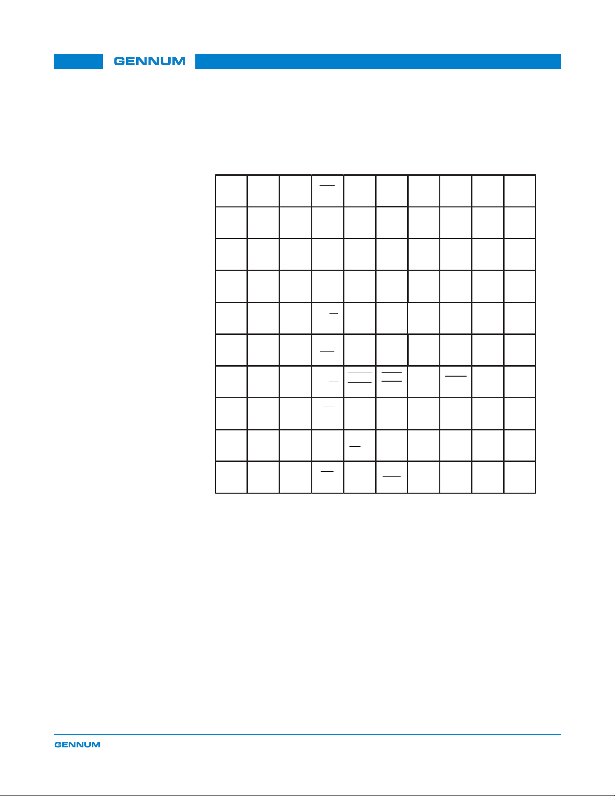
3.1 Host Interface Maps
LINE_352M_f1 1Bh Not Used Not Used Not Used Not Used Not Usedb10b9b8b7b6b5b4b3b2b1b0
30573 - 7 February 2008
1Ah
FF_LINE_START_F1 18h Not Used Not Used Not Used Not Used Not Used Not Used b9 b8 b7 b6 b5 b4 b3 b2 b1 b0
FF_LINE_END_F0 17h Not Used Not Used Not Used Not Used Not Used Not Used b9 b8 b7 b6 b5 b4 b3 b2 b1 b0
FF_LINE_START_F0 16h Not Used Not Used Not Used Not Used Not Used Not Used b9 b8 b7 b6 b5 b4 b3 b2 b1 b0
AP_LINE_END_F1 15h Not Used Not Used Not Used Not Used Not Used Not Used b9 b8 b7 b6 b5 b4 b3 b2 b1 b0
AP_LINE_START_F1 14h Not Used Not Used Not Used Not Used Not Used Not Used b9 b8 b7 b6 b5 b4 b3 b2 b1 b0
AP_LINE_END_F0 13h Not Used Not Used Not Used Not Used Not Used Not Used b9 b8 b7 b6 b5 b4 b3 b2 b1 b0
AP_LINE_START_F0 12h Not Used Not Used Not Used Not Used Not Used Not Used b9 b8 b7 b6 b5 b4 b3 b2 b1 b0
FF_LINE_END_F1 19h Not Used Not Used Not Used Not Used Not Used Not Used b9 b8 b7 b6 b5 b4 b3 b2 b1 b0
RASTER_STRUCTURE4 11h Not Used Not Used Not Used Not Used Not Usedb10b9b8b7b6b5b4b3b2b1b0
0Dh
RASTER_STRUCTURE1 0Eh Not Used Not Used Not Used Not Used b11 b10 b9 b8 b7 b6 b5 b4 b3 b2 b1 b0
RASTER_STRUCTURE3 10h Not Used Not Used Not Used Not Used Not Usedb10b9b8b7b6b5b4b3b2b1b0
RASTER_STRUCTURE2 0Fh Not Used Not Used Not Used Not Used b11 b10 b9 b8 b7 b6 b5 b4 b3 b2 b1 b0
0Ch
09h
08h
07h
06h
05h
03h
01h
VIDEO_FORMAT_B 0Bh VF4-b7 VF4-b6 VF4-b5 VF4-b4 VF4-b3 VF4-b2 VF4-b1 VF4-b0 VF3-b7 VF3-b6 VF3-b5 VF3-b4 VF3-b3 VF3-b2 VF3-b1 VF3-b0
VIDEO_FORMAT_A 0Ah VF2-b7 VF2-b6 VF2-b5 VF2-b4 VF2-b3 VF2-b2 VF2-b1 VF2-b0 VF1-b7 VF1-b6 VF1-b5 VF1-b4 VF1-b3 VF1-b2 VF1-b1 VF1-b0
VIDEO_STANDARD 04h Not Used VDS-b4 VDS-b3 VDS-b2 VDS-b1 VDS-b0 INT_PROG STD_
EDH_FLAG 02h Not Used ANC-UES ANC-IDA ANC-IDH ANC-EDA ANC-EDH FF-UES FF-IDA FF-IDH FF-EDA FF-EDH AP-UES AP-IDA AP-IDH AP-EDA AP-EDH
IOPROC_DISABLE 00h Not Used Not Used Not Used Not Used Not Used Not Used Not Used H_CONFIG Not Used 352M_INS ILLEGAL_RE
Page 20

GS1531 Data Sheet
20 of 50
LOCK
1Ch
1Bh
1Ah
19h
18h
17h
16h
15h
3.1.1 Host Interface Map (Read Only Registers)
REGISTER NAMEADDRESS1514131211109876543210
14h
13h
12h
RASTER_STRUCTURE1 0Eh b11 b10 b9 b8 b7 b6 b5 b4 b3 b2 b1 b0
RASTER_STRUCTURE3 10h b10b9b8b7b6b5b4b3b2b1b0
RASTER_STRUCTURE2 0Fh b11 b10 b9 b8 b7 b6 b5 b4 b3 b2 b1 b0
RASTER_STRUCTURE4 11h b10b9b8b7b6b5b4b3b2b1b0
30573 - 7 February 2008
0Dh
0Ch
0Bh
0Ah
09h
08h
07h
06h
05h
03h
02h
01h
00h
VIDEO_STANDARD 04h VDS-b4 VDS-b3 VDS-b2 VDS-b1 VDS-b0 INT_PROG STD_
Page 21

21 of 50
CRC_INS LNUM_ INS TRS_INS
GS1531 Data Sheet
ANC_
EDH_CRC_IN
CSUM_INS
S
MAP
1Ah
REGISTER NAMEADDRESS1514131211109876543210
LINE_352M_f2 1Ch b10b9b8b7b6b5b4b3b2b1b0
FF_LINE_END_F1 19h b9 b8 b7 b6 b5 b4 b3 b2 b1 b0
LINE_352M_f1 1Bh b10b9b8b7b6b5b4b3b2b1b0
FF_LINE_START_F1 18h b9 b8 b7 b6 b5 b4 b3 b2 b1 b0
FF_LINE_END_F0 17h b9 b8 b7 b6 b5 b4 b3 b2 b1 b0
FF_LINE_START_F0 16h b9 b8 b7 b6 b5 b4 b3 b2 b1 b0
AP_LINE_END_F1 15h b9 b8 b7 b6 b5 b4 b3 b2 b1 b0
AP_LINE_START_F1 14h b9 b8 b7 b6 b5 b4 b3 b2 b1 b0
AP_LINE_END_F0 13h b9 b8 b7 b6 b5 b4 b3 b2 b1 b0
3.1.2 Host Interface Map (R/W Configurable Registers)
AP_LINE_START_F0 12h b9 b8 b7 b6 b5 b4 b3 b2 b1 b0
11h
10h
0Fh
30573 - 7 February 2008
0Eh
0Dh
0Ch
09h
08h
07h
06h
05h
04h
03h
01h
VIDEO_FORMAT_B 0Bh VF4-b7 VF4-b6 VF4-b5 VF4-b4 VF4-b3 VF4-b2 VF4-b1 VF4-b0 VF3-b7 VF3-b6 VF3-b5 VF3-b4 VF3-b3 VF3-b2 VF3-b1 VF3-b0
VIDEO_FORMAT_A 0Ah VF2-b7 VF2-b6 VF2-b5 VF2-b4 VF2-b3 VF2-b2 VF2-b1 VF2-b0 VF1-b7 VF1-b6 VF1-b5 VF1-b4 VF1-b3 VF1-b2 VF1-b1 VF1-b0
EDH_FLAG 02h ANC-UES ANC-IDA ANC-IDH ANC-EDA ANC-EDH FF-UES FF-IDA FF-IDH FF-EDA FF-EDH AP-UES AP-IDA AP-IDH AP-EDA AP-EDH
IOPROC_DISABLE 00h H_CONFIG 352M_INS ILLEGAL_RE
Page 22

4. Detailed Description
4.1 Functional Overview
The GS1531 is a multi-rate serializer with an integrated cable driver. When used in
conjunction with the external GO1555/GO1525* Voltage Controlled Oscillator, a
transmit solution at 1.485Gb/s, 1.485/1.001Gb/s or 270Mb/s is realized.
The device has three different modes of operation which must be set through
external device pins.
When SMPTE mode is enabled, the device will accept 10-bit multiplexed or 20-bit
demultiplexed SMPTE compliant data at both HD and SD signal rates. The
device’s additional processing features are also enabled in this mode.
In DVB-ASI mode, the GS1531 will accept an 8-bit parallel DVB-ASI compliant
transport stream on its upper input bus. The serial output data stream will be
8b/10b encoded and stuffed.
The GS1531’s third mode allows for the serializing of data not conforming to
SMPTE or DVB-ASI streams.
GS1531 Data Sheet
The provided serial digital outputs feature a high impedance mode, output mute on
loss of parallel clock and adjustable signal swing. The output slew rate is
automatically controlled by the SD/HD
In the digital signal processing core, several data processing functions are
implemented including SMPTE 352M and EDH data packet generation and
insertion, and automatic video standards detection. These features are all enabled
by default, but may be individually disabled via internal registers accessible
through the GSPI host interface.
Finally, the GS1531 contains a JTAG interface for boundary scan test
implementations.
*For new designs use GO1555
4.2 Parallel Data Inputs
Data inputs enter the device on the rising edge of PCLK as shown in Figure 4-1.
The input data format is defined by the setting of the external SD/HD
SMPTE_BYPASS
format. The input data bus width is controlled independently from the internal data
bus width by the 20bit/10bit
setting.
,
and DVB_ASI pins and may be presented in 10-bit or 20-bit
input pin.
30573 - 7 February 2008 22 of 50
Page 23

Figure 4-1: PCLK to Data Timing
PCLK
DIN[19:0]
DATA
Control signal
input
tSU
tIH
4.2.1 Parallel Input in SMPTE Mode
When the device is operating in SMPTE mode, see SMPTE Mode on page 25, both
SD and HD data may be presented to the input bus in either multiplexed or
demultiplexed form depending on the setting of the 20bit/10bit
GS1531 Data Sheet
input pin.
In 20-bit mode, (20bit/10bit
demultiplexed luma and chroma data. Luma words should be presented to
DIN[19:10] while chroma words should occupy DIN[9:0].
In 10-bit mode, (20bit/10bit
multiplexed luma and chroma data. The data should be presented to DIN[19:10].
DIN[9:0] will be high impedance in this mode.
4.2.2 Parallel Input in DVB-ASI Mode
When operating in DVB-ASI mode, see DVB-ASI mode on page 26, the GS1531
requires the input data bus to be configured for 10-bit operation (20bit/10bit
LOW).
The device accepts 8-bit data words on DIN[17:10] such that DIN17 = HIN is the
most significant bit of the encoded transport stream data and DIN10 = AIN is the
least significant bit.
In addition, DIN19 and DIN18 are configured as the DVB-ASI control signals
INSSYNCIN and KIN respectively. See DVB-ASI mode on page 26 for a
description of these DVB-ASI specific input signals.
The pins DIN[9:0] are high impedance when the GS1531 is operating in DVB-ASI
mode.
= HIGH), the input data format should be word aligned,
= LOW), the input data format should be word aligned,
=
4.2.3 Parallel Input in Data-Through Mode
When operating in Data-Through mode, see Data-Through Mode on page 28, the
GS1531 passes data presented to the parallel input bus to the serial output without
performing any encoding or scrambling.
The input data bus width accepted by the device in this mode is controlled by the
setting of the 20bit/10bit
30573 - 7 February 2008 23 of 50
pin.
Page 24

4.2.4 Parallel Input Clock (PCLK)
The frequency of the PCLK input signal required by the GS1531 is determined by
the input data format. Table 4-1 below lists the possible input signal formats and
their corresponding parallel clock rates.
GS1531 Data Sheet
NOTE: DVB-ASI input requires a 10-bit wide input data bus (20bit/10bit
Table 4-1: Parallel Data Input Format
Control Signals
Input Data Format DIN
[19:10]
SMPTE MODE
20bit DEMULTIPLEXED SD LUMA CHROMA 13.5MHz HIGH HIGH HIGH LOW
10bit MULTIPLEXED SD LUMA /
CHROMA
20bit DEMULTIPLEXED HD LUMA CHROMA 74.25 or
10bit MULTIPLEXED HD LUMA /
CHROMA
DVB-ASI MODE
10bit DVB-ASI DVB-ASI
DATA
DIN [9:0] PCLK
HIGH
IMPEDANCE
HIGH
IMPEDANCE
HIGH
IMPEDANCE
27MHz LOW HIGH HIGH LOW
74.25/
1.001MHz
148.5 or
148.5/
1.001MHz
27MHz LOW HIGH LOW HIGH
20bit/
10bit
HIGH LOW HIGH LOW
LOW LOW HIGH LOW
LOW HIGH LOW HIGH
SD/
HD
SMPTE_BYPASS DVB_ASI
= LOW).
DATA-THROUGH MODE
20bit DEMULTIPLEXED SD DATA DATA 13.5MHz HIGH HIGH LOW LOW
10bit MULTIPLEXED SD DATA HIGH
IMPEDANCE
20bit DEMULTIPLEXED HD DATA DATA 74.25 or
10bit MULTIPLEXED HD DATA HIGH
IMPEDANCE
30573 - 7 February 2008 24 of 50
27MHz LOW HIGH LOW LOW
HIGH LOW LOW LOW
74.25/
1.001MHz
148.5 or
148.5/
1.001MHz
LOW LOW LOW LOW
Page 25

4.3 SMPTE Mode
4.3.1 Internal Flywheel
GS1531 Data Sheet
The GS1531 is said to be in SMPTE mode when the SMPTE_BYPASS pin is set
HIGH and the DVB_ASI pin is set LOW.
In this mode, the parallel data will be scrambled according to SMPTE 259M or
292M, and NRZ-to-NRZI encoded prior to serialization.
The GS1531 has an internal flywheel which is used in the generation of internal /
external timing signals, and in automatic video standards detection. It is
operational in SMPTE mode only.
The flywheel consists of a number of counters and comparators operating at video
pixel and video line rates. These counters maintain information about the total line
length, active line length, total number of lines per field / frame and total active lines
per field / frame for the received video standard.
When DETECT_TRS is LOW, the flywheel will be locked to the externally supplied
H, V, and F timing signals.
When DETECT_TRS is HIGH, the flywheel will be locked to the embedded TRS
signals in the parallel input data. Both 8-bit and 10-bit TRS code words will be
identified by the device.
The flywheel 'learns' the video standard by timing the horizontal and vertical
reference information supplied a the H, V, and F input pins, or contained in the TRS
ID words of the received video data. Full synchronization of the flywheel to the
received video standard therefore requires one complete video frame.
Once synchronization has been achieved, the flywheel will continue to monitor the
received TRS timing or the supplied H, V, and F timing information to maintain
synchronization.
4.3.2 HVF Timing Signal Extraction
As discussed above, the GS1531's internal flywheel may be locked to externally
provided H, V, and F signals when DETECT_TRS is set LOW.
The H signal timing should also be configured via the H_CONFIG bit of the internal
IOPROC_DISABLE register as either active line based blanking or TRS based
blanking, see Packet Generation and Insertion on page 30.
Active line based blanking is enabled when the H_CONFIG bit is set LOW. In this
mode, the H input should be HIGH for the entire horizontal blanking period,
including the EAV and SAV TRS words. This is the default H timing assumed by
the device.
When H_CONFIG is set HIGH, TRS based blanking is enabled. In this case, the H
input should be set HIGH for the entire horizontal blanking period as indicated by
the H bit in the associated TRS words.
The timing of these signals is shown in Figure 4-2.
30573 - 7 February 2008 25 of 50
Page 26

GS1531 Data Sheet
H:V:F TIMING - HD 20-BIT INPUT MODE
PCLK
LUMA DATA OUT
CHROMA DATA OUT
H
XYZ
(eav)
0000003FF
XYZ
(eav)
0000003FF
V
F
XYZ
(sav)
0000003FF
XYZ
(sav)
0000003FF
H;V:F TIMING AT SAV - HD 10-BIT INPUT MODE
0000003FF3FF
XYZ
(sav)
000000
XYZ
(sav)
PCLK
H
V
F
H:V:F TIMING AT EAV - HD 10-BIT INPUT MODE
PCLK
0000003FF3FF
XYZ
(eav)
000000
XYZ
(eav)
MULTIPLEXED
Y/Cr/Cb DATA OUT
H
V
F
MULTIPLEXED
Y/Cr/Cb DATA OUT
H:V:F TIMING - SD 20-BIT INPUT MODE
PCLK
CHROMA DATA OUT
LUMA DATA OUT
H
0003FF
XYZ
(eav)
000
V
F
0003FF
XYZ
(SAV)
000
H:V:F TIMING - SD 10-BIT INPUT MODE
MULTIPLEXED
Y/Cr/Cb DATA OUT
PCLK
H
V
F
XYZ
(eav)
0000003FF
XYZ
(sav)
0000003FF
H SIGNAL TIMING:
H_CONFIG = LOW
H_CONFIG = HIGH
4.4 DVB-ASI mode
Figure 4-2: H, V, F Timing
To operate the GS1531 in DVB-ASI mode, set the SMPTE_BYPASS and
20bit/10bit
pins LOW, and the DVB_ASI and SD/HD pins HIGH.
30573 - 7 February 2008 26 of 50
Page 27

4.4.1 Control Signal Inputs
8
8
AIN ~ HIN
PCLK = 27MHz
INSSYNCIN
SDO
CLK_IN
CLK_OUT
FIFO
SDO
WRITE_CLK
<27MHz
FE
TS
KIN
GS1531
KIN
READ CLK
=27MHz
In DVB-ASI mode, the DIN19 and DIN18 pins will be configured as DVB-ASI
control signals INSSYNCIN and KIN respectively.
When INSSYNCIN is set HIGH, the device will insert K28.5 sync characters into
the data stream. This function is used to assist system implementations where the
GS1531 may be preceded by an external data FIFO. Parallel DVB-ASI data may
be clocked into the FIFO at some rate less than 27MHz. The INSSYNCIN input
may then be connected to the FIFO empty signal, thus providing a means of
padding up the data transmission rate to 27MHz. See Figure 4-3.
NOTE: 8b/10b encoding will take place after K28.5 sync character insertion.
KIN should be set HIGH whenever the parallel data input is to be interpreted as any
special character defined by the DVB-ASI standard (including the K28.5 sync
character). This pin should be set LOW when the input is to be interpreted as data.
NOTE: When operating in DVB-ASI mode, DIN[9:0] become high impedance.
GS1531 Data Sheet
Figure 4-3: DVB-ASI FIFO Implementation using the GS1531
30573 - 7 February 2008 27 of 50
Page 28

4.5 Data-Through Mode
The GS1531 may be configured to operate as a simple parallel-to-serial converter.
In this mode, the device presents data to the output buffer without performing any
scrambling or encoding.
GS1531 Data Sheet
Data-through mode is enabled only when both the SMPTE_BYPASS
DVB_ASI pins are set LOW.
4.6 Additional Processing Functions
The GS1531 contains an additional data processing block which is available in
SMPTE mode only, see SMPTE Mode on page 25.
4.6.1 Input Data Blank
The video input data may be 'blanked' by the GS1531. In this mode, all input video
data except TRS words are set to the appropriate blanking levels by the device.
Both the horizontal and vertical ancillary data spaces will also be set to blanking
levels.
This function is enabled by setting the BLANK
4.6.2 Automatic Video Standard Detection
The GS1531 can detect the input video standard by using the timing parameters
extracted from the received TRS ID words or supplied H, V, and F timing signals,
see Internal Flywheel on page 25. This information is presented to the host
interface via the VIDEO_STANDARD register (Table 4-2).
and
pin LOW.
Total samples per line, active samples per line, total lines per field/frame and active
lines per field/frame are also calculated and presented to the host interface via the
RASTER_STRUCTURE registers (Table 4-3). These line and sample count
registers are updated once per frame at the end of line 12. This is in addition to the
information contained in the VIDEO_STANDARD register.
After device reset, the four RASTER_STRUCTURE registers default to zero.
Table 4-2: Host Interface Description for Video Standard Register
Register Name Bit Name Description R/W Default
VIDEO_STANDARD
Address: 004h
15 – Not Used. – –
14-10 VD_STD[4:0] Video Data Standard (see Table 4-4). R 0
9 INT_PROG
8 STD_LOCK Standard Lock: Set HIGH when flywheel has
7-0 – Not Used. – –
30573 - 7 February 2008 28 of 50
Interlace/Progressive: Set LOW if detected video
standard is PROGRESSIVE and is set HIGH if it is
INTERLACED.
achieved full synchronization.
R0
R0
Page 29

GS1531 Data Sheet
Table 4-3: Host Interface Description for Raster Structure Registers
Register Name Bit Name Description R/W Default
RASTER_STRUCTURE1
Address: 00Eh
RASTER_STRUCTURE2
Address: 00Fh
RASTER_STRUCTURE3
Address: 010h
RASTER_STRUCTURE4
Address: 011h
15-12 – Not Used. – –
11-0 RASTER_STRUCTURE_1[11:0] Words Per Active Line R 0
15-13 – Not Used. – –
12-0 RASTER_STRUCTURE_2[12:0] Words Per Total Line. R 0
15-11 – Not Used. – –
10-0 RASTER_STRUCTURE_3[10:0] Total Lines Per Frame R 0
15-11 – Not Used. – –
10-0 RASTER_STRUCTURE_4[10:0] Active Lines Per Field R 0
4.6.2.1 Video Standard Indication
The video standard codes reported in the VD_STD[4:0] bits of the
VIDEO_STANDARD register represent the SMPTE standards as shown in
Table 4-4.
In addition to the 5-bit video standard code word, the VIDEO_STANDARD register
also contains two status bits. The STD_LOCK bit will be set HIGH whenever the
flywheel has achieved full synchronization. The INT_PROG bit will be set LOW if
the detected video standard is progressive and HIGH if the detected video
standard is interlaced.
The VD_STD[4:0], STD_LOCK and INT_PROG
bits of the VIDEO_STANDARD
register will default to zero after device reset. The VD_STD[4:0] and INT_PROG
bits will also default to zero if the SMPTE_BYPASS
pin is asserted LOW or if the
LOCKED output is LOW. The STD_LOCK bit will retain its previous value if the
PCLK is removed.
Table 4-4: Supported Video Standards
VD_STD[4:0] SMPTE
Standard
00h 296M (HD) 1280x720/60 (1:1) 358 1280 1650 10
01h 296M (HD) 1280x720/60 (1:1) - EM 198 1440 1650 10
02h 296M (HD) 1280x720/30 (1:1) 2008 1280 3300 10
03h 296M (HD) 1280x720/30 (1:1) - EM 408 2880 3300 10
04h 296M (HD) 1280x720/50 (1:1) 688 1280 1980 10
05h 296M (HD) 1280x720/50 (1:1) - EM 240 1728 1980 10
06h 296M (HD) 1280x720/25 (1:1) 2668 1280 3960 10
07h 296M (HD) 1280x720/25 (1:1) - EM 492 3456 3960 10
Video Format Length of
HANC
Length of
Active Video
Total
Samples
SMPTE352M
Lines
30573 - 7 February 2008 29 of 50
Page 30

Table 4-4: Supported Video Standards (Continued)
GS1531 Data Sheet
VD_STD[4:0] SMPTE
Standard
08h 296M (HD) 1280x720/24 (1:1) 2833 1280 4125 10
09h 296M (HD) 1280x720/24 (1:1) - EM 513 3600 4125 10
0Ah 274M (HD) 1920x1080/60 (2:1) or
0Bh 274M (HD) 1920x1080/30 (1:1) 268 1920 2200 18
0Ch 274M (HD) 1920x1080/50 (2:1) or
0Dh 274M (HD) 1920x1080/25 (1:1) 708 1920 2640 18
0Eh 274M (HD) 1920x1080/25 (1:1) - EM 324 2304 2640 18
0Fh 274M (HD) 1920x1080/25 (PsF) - EM 324 2304 2640 10, 572
10h 274M (HD) 1920x1080/24 (1:1) 818 1920 2750 18
11h 274M (HD) 1920x1080/24 (PsF) 818 1920 2750 10, 572
12h 274M (HD) 1920x1080/24 (1:1) - EM 338 2400 2750 18
13h 274M (HD) 1920x1080/24 (PsF) - EM 338 2400 2750 10, 572
14h 295M (HD) 1920x1080/50 (2:1) 444 1920 2376 10, 572
15h 260M (HD) 1920x1035/60 (2:1) 268 1920 2200 10, 572
Video Format Length of
HANC
268 1920 2200 10, 572
1920x1080/30 (PsF)
708 1920 2640 10, 572
1920x1080/25 (PsF)
Length of
Active Video
Total
Samples
SMPTE352M
Lines
16h 125M (SD) 1440x487/60 (2:1)
(Or dual link progressive)
17h 125M (SD) 1440x507/60 (2:1) 268 1440 1716 10, 276
19h 125M (SD) 525-line 487 generic – – 1716 10, 276
1Bh 125M (SD) 525-line 507 generic – – 1716 10, 276
18h ITU-R BT.656
(SD)
1Ah ITU-R BT.656
(SD)
1Dh Unknown HD – – – – –
1Eh Unknown SD – – – – –
1Ch, 1Fh Reserved – – – – –
NOTE: Though the GS1531 will work correctly on and serialize both 59.94Hz and 60Hz formats, it will not distinguish between them.
1440x576/50 (2:1)
(Or dual link progressive)
625-line generic (EM) – – 1728 9, 322
268 1440 1716 10, 276
280 1440 1728 9, 322
4.6.3 Packet Generation and Insertion
In addition to input data blanking and automatic video standards detection, the
GS1531 may also calculate, assemble and insert into the data stream various
types of ancillary data packets and TRS ID words.
30573 - 7 February 2008 30 of 50
Page 31

GS1531 Data Sheet
These features are only available when the device is set to operated in SMPTE
mode and the IOPROC_EN/DIS
pin is set HIGH. Individual insertion features may
be enabled or disabled via the IOPROC_DISABLE register (Table 4-5).
All of the IOPROC_DISABLE register bits default to '0' after device reset, enabling
all of the processing features. To disable any individual error correction feature, the
host interface must set the corresponding bit HIGH in this register.
Table 4-5: Host Interface Description for Internal Processing Disable Register
Register Name Bit Name Description R/W Default
IOPROC_DISABLE
Address: 000h
15-9 – Not Used. – –
8 H_CONFIG Horizontal sync timing input configuration. Set LOW
when the H input timing is based on active line
blanking (default). Set HIGH when the H input
timing is based on the H bit of the TRS words. See
Figure 4-2.
7 – Not Used. – –
6 352M_INS SMPTE352M packet insertion. In HD mode, 352M
packets are inserted in the Y channel only when one
of the bytes in the VIDEO_FORMAT_A or
VIDEO_FORMAT_B registers are programmed with
non-zero values. The IOPROC_EN/DIS pin and
SMPTE_BYPASS
HIGH to disable.
5 ILLEGAL_REMAP Illegal Code Remapping. Detection and correction
of illegal code words within the active picture area
(AP). The IOPROC_EN/DIS
SMPTE_BYPASS
HIGH to disable.
4 EDH_CRC_INS Error Detection & Handling (EDH) Cyclical
Redundancy Check (CRC) error correction. In SD
mode the GS1531 will generate and insert EDH
packets. The IOPROC_EN/DIS
SMPTE_BYPASS
HIGH to disable.
3 ANC_CSUM_INS Ancillary Data Checksum insertion. The
IOPROC_EN/DIS
must also be set HIGH. Set HIGH to disable.
2 CRC_INS Y and C line-based CRC insertion. In HD mode,
line-based CRC words are inserted in both the Y
and C channels. The IOPROC_EN/DIS
SMPTE_BYPASS
HIGH to disable
1 LNUM_INS Y and C line number insertion - HD mode only. The
IOPROC_EN/DIS
must be set HIGH. Set HIGH to disable.
0 TRS_INS Timing Reference Signal Insertion. Occurs only
when IOPROC_EN/DIS
SMPTE_BYPASS
pin must also be set HIGH. Set
pin and
pin must also be set HIGH. Set
pin and
pin must also be set HIGH. Set
pin and SMPTE_BYPASS pin
pin and
pin must be also set HIGH. Set
pin and SMPTE_BYPASS pin
is HIGH and
is HIGH. Set HIGH to disable.
R/W 0
R/W 0
R/W 0
R/W 0
R/W 0
R/W 0
R/W 0
R/W 0
30573 - 7 February 2008 31 of 50
Page 32

4.6.3.1 SMPTE 352M Payload Identifier Insertion
The GS1531 can generate and insert SMPTE 352M payload identifier ancillary
data packets into the data stream, based on information programmed into the host
interface.
When this feature is enabled, the device will automatically generate the ancillary
data preambles, (DID, SDID, DBN, DC), and calculate the checksum. The SMPTE
352M packet will be inserted into the data stream according to the line numbers
programmed in the LINE_352M registers (Table 4-6).
The insertion process will only take place if one or more of the four
VIDEO_FORMAT registers (Table 4-7) have been programmed with non-zero
values. In addition, the GS1531 requires the 352M_INS bit of the
IOPROC_DISABLE register be set LOW.
NOTE 1: For the purpose of determining the line and pixel position for insertion, the
GS1531 will differentiate between PsF and interlaced formats by interrogating bits
14 and 15 of the VIDEO_FORMAT_A register.
The packets will be inserted immediately after the EAV word in SD video streams
and immediately after the line-based CRC word in the Y channel of HD video
streams.
GS1531 Data Sheet
NOTE 2: It is the responsibility of the user to ensure that there is sufficient space
in the horizontal blanking interval for the insertion of the SMPTE 352M packets.
If there are other ancillary data packets present, the SMPTE 352M packet will be
inserted in the first available location in the horizontal ancillary space. Ancillary
data must be adjacent to the EAV in SD streams or to the line based-CRC in HD
streams. Where there is insufficient space available, the 352M packets will not be
inserted.
Table 4-6: Host Interface Description for SMPTE 352M Packet Line Number Insertion Registers
Register Name Bit Name Description R/W Default
LINE_352M_f1
Address: 01Bh
LINE_352M_f2
Address: 01Ch
15-11 – Not Used. – –
10-0 LINE_0_352M[10:0] Line number where SMPTE352M packet is inserted
in field 1.
15-11 – Not Used. – –
10-0 LINE_1_352M[10:0] Line number where SMPTE352M packet is inserted
in field 2.
R/W 0
R/W 0
30573 - 7 February 2008 32 of 50
Page 33

GS1531 Data Sheet
Table 4-7: Host Interface Description for SMPTE 352M Payload Identifier Registers
Register Name Bit Name Description R/W Default
VIDEO_FORMAT_B
Address: 00Bh
VIDEO_FORMAT_A
Address: 00Ah
15-8 SMPTE352M
Byte 4
7-0 SMPTE352M
Byte 3
15-8 SMPTE352M
Byte 2
7-0 SMPTE 352M
Byte 1
4.6.3.2 Illegal Code Remapping
If the ILLEGAL_REMAP bit of the IOPROC_DISABLE register is set LOW, the
GS1531 will remap all codes within the active picture between the values of 3FCh
and 3FFh to 3FBh. All codes within the active picture area between the values of
000h and 003h will be remapped to 004h.
In addition, 8-bit TRS and ancillary data preambles will be remapped to 10-bit
values if this feature is enabled.
4.6.3.3 EDH Generation and Insertion
SMPTE 352M Byte 4 information must be
programmed in this register when 352M_INS =
LOW.
SMPTE 352M Byte 3 information must be
programmed in this register when 352M_INS =
LOW.
SMPTE 352M Byte 2 information must be
programmed in this register when 352M_INS =
LOW.
SMPTE 352M Byte 1 information must be
programmed in this register when 352M_INS =
LOW.
R/W 0
R/W 0
R/W 0
R/W 0
When operating in SD mode, (SD/HD
= HIGH), the GS1531 will generate and
insert complete EDH packets into the data stream. Packet generation and insertion
will only take place if the EDH_CRC_INS bit of the IOPROC_DISABLE register is
set LOW.
The GS1531 will generate all of the required EDH packet data including all ancillary
data preambles, (DID, DBN, DC), reserved code words and checksum. Calculation
of both full field (FF) and active picture (AP) CRC's will be carried out by the device.
SMPTE RP165 specifies the calculation ranges and scope of EDH data for
standard 525 and 625 component digital interfaces. The GS1531 will utilize these
standard ranges by default.
If the received video format does not correspond to 525 or 625 digital component
video standards as determined by the flywheel pixel and line counters, then one of
two schemes for determining the EDH calculation ranges will be employed:
1. Ranges will be based on the line and pixel ranges programmed by the host
interface; or
2. In the absence of user-programmed calculation ranges, ranges will be
determined from the received TRS ID words or supplied H, V, and F timing
signals, see Internal Flywheel on page 25.
30573 - 7 February 2008 33 of 50
Page 34

GS1531 Data Sheet
The registers available to the host interface for programming EDH calculation
ranges include active picture and full field line start and end positions for both
fields. Table 4-8 shows the relevant registers, which default to '0' after device reset.
If any or all of these register values are zero, then the EDH CRC calculation ranges
will be determined from the flywheel generated H signal. The first active and full
field pixel will always be the first pixel after the SAV TRS code word. The last active
and full field pixel will always be the last pixel before the start of the EAV TRS code
words.
EDH error flags (EDH, EDA, IDH, IDA and UES) for ancillary data, full field and
active picture will also be inserted. These flags must be programmed into the
EDH_FLAG registers of the device (Table 4-9).
NOTE 1: It is the responsibility of the user to ensure that the EDH flag registers are
updated once per field.
The prepared EDH packet will be inserted at the appropriate line of the video
stream according to RP165. The start pixel position of the inserted packet will be
based on the SAV position of that line such that the last byte of the EDH packet
(the checksum) will be placed in the sample immediately preceding the start of the
SAV TRS word.
NOTE 2: It is also the responsibility of the user to ensure that there is sufficient
space in the horizontal blanking interval for the EDH packet to be inserted.
Table 4-8: Host Interface Description for EDH Calculation Range Registers
Register Name Bit Name Description R/W Default
AP_LINE_START_F0
Address: 012h
AP_LINE_END_F0
Address: 013h
AP_LINE_START_F1
Address: 014h
AP_LINE_END_F1
Address: 015h
15-10 – Not Used. – –
9-0 AP_LINE_START_F0[9:0] Field 0 Active Picture start line data used to set
EDH calculation range outside of RP 165
values.
15-10 – Not Used. – –
9-0 AP_LINE_END_F0[9:0] Field 0 Active Picture end line data used to set
EDH calculation range outside of RP 165
values.
15-10 – Not Used. – –
9-0 AP_LINE_START_F1[9:0] Field 1 Active Picture start line data used to set
EDH calculation range outside of RP 165
values.
15-10 – Not Used. – –
9-0 AP_LINE_END_F1[9:0] Field 1 Active Picture end line data used to set
EDH calculation range outside of RP 165
values.
R/W 0
R/W 0
R/W 0
R/W 0
30573 - 7 February 2008 34 of 50
Page 35

GS1531 Data Sheet
Table 4-8: Host Interface Description for EDH Calculation Range Registers (Continued)
Register Name Bit Name Description R/W Default
FF_LINE_START_F0
Address: 016h
FF_LINE_END_F0
Address: 017h
FF_LINE_START_F1
Address: 018h
FF_LINE_END_F1
Address: 019h
Table 4-9: Host Interface Description for EDH Flag Register
15-10 – Not Used. – –
9-0 FF_LINE_START_F0[9:0] Field 0 Full Field start line data used to set EDH
calculation range outside of RP 165 values.
15-10 – Not Used. – –
9-0 FF_LINE_END_F0[9:0] Field 0 Full Field end line data used to set EDH
calculation range outside of RP 165 values.
15-10 – Not Used. – –
9-0 FF_LINE_START_F1[9:0] Field 1 Full Field start line data used to set EDH
calculation range outside of RP-165 values.
15-10 – Not Used. – –
9-0 FF_LINE_END_F1[9:0] Field 1 Full Field end line data used to set EDH
calculation range outside of RP-165 values.
R/W 0
R/W 0
R/W 0
R/W 0
Register Name Bit Name Description R/W Default
EDH_FLAG
Address: 002h
15 – Not Used. – –
14 ANC-UES Ancillary Unknown Error Status flag will be
generated and inserted when
IOPROC_EN/DIS
are HIGH and EDH_CRC_INS bit is LOW. SD
mode only.
and SMPTE_BYPASS pins
R/W 0
13 ANC-IDA Ancillary Internal device error Detected Already
flag will be generated and inserted when
IOPROC_EN/DIS
are HIGH and EDH_CRC_INS bit is LOW. SD
mode only.
12 ANC-IDH Ancillary Internal device error Detected Here
flag will be generated and inserted when
IOPROC_EN/DIS
are HIGH and EDH_CRC_INS bit is LOW. SD
mode only.
11 ANC-EDA Ancillary Error Detected Already flag will be
generated and inserted when
IOPROC_EN/DIS
are HIGH and EDH_CRC_INS bit is LOW. SD
mode only.
10 ANC-EDH Ancillary Error Detected Here flag will be
generated and inserted when
IOPROC_EN/DIS
are HIGH and EDH_CRC_INS bit is LOW. SD
mode only.
30573 - 7 February 2008 35 of 50
and SMPTE_BYPASS pins
and SMPTE_BYPASS pins
and SMPTE_BYPASS pins
and SMPTE_BYPASS pins
R/W 0
R/W 0
R/W 0
R/W 0
Page 36

GS1531 Data Sheet
Table 4-9: Host Interface Description for EDH Flag Register (Continued)
Register Name Bit Name Description R/W Default
9 FF-UES Full Field Unknown Error flag will be generated
and inserted when IOPROC_EN/DIS
SMPTE_BYPASS
EDH_CRC_INS bit is LOW. SD mode only.
8 FF-IDA Full Field Internal device error Detected
Already flag will be generated and inserted
when IOPROC_EN/DIS
pins are HIGH and EDH_CRC_INS bit is LOW.
SD mode only.
7 FF-IDH Full Field Internal device error Detected flag will
be generated and inserted when
IOPROC_EN/DIS
are HIGH and EDH_CRC_INS bit is LOW. SD
mode only.
6 FF-EDA Full Field Error Detected Already flag will be
generated and inserted when
IOPROC_EN/DIS
are HIGH and EDH_CRC_INS bit is LOW. SD
mode only.
5 FF-EDH Full Field Error Detected Here flag will be
generated and inserted when
IOPROC_EN/DIS
are HIGH and EDH_CRC_INS bit is LOW. SD
mode only.
4 AP-UES Active Picture Unknown Error Status flag will be
generated and inserted when
IOPROC_EN/DIS
are HIGH and EDH_CRC_INS bit is LOW. SD
mode only.
pins are HIGH and
and SMPTE_BYPASS
and SMPTE_BYPASS pins
and SMPTE_BYPASS pins
and SMPTE_BYPASS pins
and SMPTE_BYPASS pins
and
R/W 0
R/W 0
R/W 0
R/W 0
R/W 0
R/W 0
3 AP-IDA Active Picture Internal device error Detected
2 AP-IDH Active Picture Internal device error Detected
1 AP-EDA Active Picture Error Detected Already flag will
0 AP-EDH Active Picture Error Detected Here flag will be
30573 - 7 February 2008 36 of 50
Already flag will be generated and inserted
when IOPROC_EN/DIS
pins are HIGH and EDH_CRC_INS bit is LOW.
SD mode only.
Here flag will be generated and inserted when
IOPROC_EN/DIS
are HIGH and EDH_CRC_INS bit is LOW. SD
mode only.
be generated and inserted when
IOPROC_EN/DIS
are HIGH and EDH_CRC_INS bit is LOW. SD
mode only.
generated and inserted when
IOPROC_EN/DIS
are HIGH and EDH_CRC_INS bit is LOW. SD
mode only.
and SMPTE_BYPASS
and SMPTE_BYPASS pins
and SMPTE_BYPASS pins
and SMPTE_BYPASS pins
R/W 0
R/W 0
R/W 0
R/W 0
Page 37

4.6.3.4 Ancillary Data Checksum Generation and Insertion
The GS1531 will calculate checksums for all detected ancillary data packets
presented to the device. These calculated checksum values are inserted into the
data stream prior to serialization.
Ancillary data checksum generation and insertion will only take place if the
ANC_CSUM_INS bit of the IOPROC_DISABLE register is set LOW.
4.6.3.5 Line Based CRC Generation and Insertion
The GS1531 will generate and insert line based CRC words into both the Y and C
channels of the data stream. This feature is only available in HD mode and is
enabled by setting the CRC_INS bit of the IOPROC_DISABLE register LOW.
4.6.3.6 HD Line Number Generation and Insertion
In HD mode, the GS1531 will calculate and insert line numbers into the Y and C
channels of the output data stream.
Line number generation is in accordance with the relevant HD video standard as
determined by the device, see Automatic Video Standard Detection on page 28.
GS1531 Data Sheet
This feature is enabled when SD/HD
IOPROC_DISABLE register is set LOW.
4.6.3.7 TRS Generation and Insertion
The GS1531 can generate and insert 10-bit TRS code words into the data stream
as required. This feature is enabled by setting the TRS_INS bit of the
IOPROC_DISABLE register LOW.
TRS word generation will be performed in accordance with the timing parameters
generated by the flywheel which will be locked either to the received TRS ID words
or the supplied H, V, and F timing signals, see Internal Flywheel on page 25.
4.7 Parallel-To-Serial Conversion
The parallel data output of the internal data processing blocks is fed to the
parallel-to-serial converter. The function of this block is to generate a serial data
stream from the 10-bit or 20-bit parallel data words and pass the stream to the
integrated cable driver.
= LOW, and the LNUM_INS bit of the
30573 - 7 February 2008 37 of 50
Page 38

4.8 Serial Digital Data PLL
To obtain a clean clock signal for serialization and transmission, the input PCLK is
locked to an external reference signal via the GS1531's integrated phase-locked
loop. This high quality analog PLL allows the GS1531 to significantly attenuate jitter
on the incoming PCLK. This PLL is also responsible for generating all internal clock
signals required by the device.
Internal division ratios for the locked PCLK are determined by the setting of the
SD/HD
Table 4-10: Serial Digital Output Rates
and 20bit/10bit pins as shown in Table 4-10.
GS1531 Data Sheet
4.8.1 External VCO
Supplied PCLK Rate Serial Digital
Output Rate
74.25 or
74.25/1.001 MHz
148.5 or
148.5/1.001MHz
13.5MHz 270Mb/s HIGH HIGH
27MHz 270Mb/s HIGH LOW
1.485 or
1.485/1.001Gb/s
1.485 or
1.485/1.001Gb/s
SD/HD 20bit/10bit
Pin Settings
LOW HIGH
LOW LOW
The GS1531 requires the GO1555/GO1525* external voltage controlled oscillator
as part of its internal PLL.
Power for the external VCO is generated entirely by the GS1531 from an integrated
voltage regulator. The internal regulator uses +3.3V supplied on the CP_VDD /
CP_GND pins to provide +2.5V on the VCO_VCC / VCO_GND pins.
The external VCO produces a 1.485GHz reference signal for the PLL, input on the
VCO pin of the device. Both reference and control signals should be referenced to
the supplied VCO_GND as shown in the recommended application circuit of
Typical Application Circuit on page 46.
*For new designs use GO1555
4.8.2 Lock Detect Output
The lock detect block controls the serial digital output signal and indicates the lock
status of the device via the LOCKED output pin.
LOCKED will be asserted HIGH if and only if the internal data PLL has locked the
PCLK signal to the external VCO reference signal and one of the following is true:
1. The device is set to operate in SMPTE mode and has detected SMPTE TRS
2. The device is set to operate in DVB-ASI mode and has detected K28.5 sync
30573 - 7 February 2008 38 of 50
words in the serial stream; or
characters in the serial stream; or
Page 39

3. The device is set to operate in Data-Through mode.
4.8.3 Loop Bandwidth Adjustment
For new designs the GO1555 is recommended for use with the GS1531. The
recommended loop bandwidth control component values are listed in Table 4-11
and can be seen in Section 5.1 Typical Application Circuit.
Designs using the GO1525 VCO will require different loop bandwidth control
components. The component values are listed in Table 4-11.
Table 4-11: GO1555 Loop Bandwidth Adjustment
Component GO1555 GO1525
LB_CONT 100nF 100nF
GS1531 Data Sheet
NOTE: When using the GS1531 with the GS4911B clock generator a narrower
loop bandwidth for the GS1531 serializer should be used. For more details please
refer to Section 2.5 of the GS4911B Reference Design.
4.9 Serial Digital Output
The GS1531 contains an integrated current mode differential serial digital cable
driver with automatic slew rate control.
The integrated cable driver uses a separate power supply of +1.8V DC supplied via
the CD_VDD and CD_GND pins.
To enable the output, SDO_EN/DIS
signal LOW will cause the SDO and SDO
resulting in reduced device power consumption.
Gennum recommends using the GS1528A SDI Dual Slew-Rate Cable Driver to
meet SMPTE specifications.
R
LF-CP_CAP
CP_CAP 47nF 22nF
33Ω 50Ω
must be set HIGH. Setting the SDO_EN/DIS
output pins to become high impedance,
4.9.1 Output Swing
Nominally, the voltage swing of the serial digital output is 800mVp-p single-ended
into a 75Ω load. This is set externally by connecting the RSET pin to CD_VDD
through 281Ω .
The output swing may be decreased by increasing the value of the RSET resistor.
The relationship is approximated by the curve shown in Figure 4-4.
Alternatively, the serial digital output swing can drive 800mVp-p into a 50Ω load.
Since the output swing is reduced by a factor of approximately one third when the
smaller load is used, the RSET resistor must be 187Ω to obtain 800mVp-p.
30573 - 7 February 2008 39 of 50
Page 40

1000
900
800
700
(mVp-p)
600
SDO
ΔV
500
400
300
GS1531 Data Sheet
75Ω load
50Ω load
200
Figure 4-4: Serial Digital Output Swing
4.9.2 Serial Digital Output Mute
The GS1531 will automatically mute the serial digital output when the LOCKED
output signal is LOW. In this case, the SDO and SDO
voltage level.
4.10 GSPI Host Interface
The GSPI, or Gennum Serial Peripheral Interface, is a 4-wire interface provided to
allow the host to enable additional features of the device and /or to provide
additional status information through configuration registers in the GS1531.
The GSPI comprises a serial data input signal SDIN, serial data output signal
SDOUT, an active low chip select CS
must have a duty cycle between 40% and 60%.
Because these pins are shared with the JTAG interface port, an additional control
signal pin JTAG/HOST
is enabled.
250
300
350
400
450
RSET(Ω)
500
550
600
650
700
signals are set to a constant
, and a burst clock SCLK. The burst clock
is provided. When JTAG/HOST is LOW, the GSPI interface
When operating in GSPI mode, the SCLK, SDIN, and CS
signals are provided by
the host interface. The SDOUT pin is a high-impedance output allowing multiple
devices to be connected in parallel and selected via the CS
input. The interface is
illustrated in the Figure 4-5 below.
All read or write access to the GS1531 is initiated and terminated by the host
processor. Each access always begins with a 16-bit command word on SDIN
indicating the address of the register of interest. This is followed by a 16-bit data
word on SDIN in write mode, or a 16-bit data word on SDOUT in read mode.
30573 - 7 February 2008 40 of 50
Page 41

Figure 4-5: Gennum Serial Peripheral Interface (GSPI)
SCLK
CS
SDOUT
SDIN
SCLK
CS
SDIN
SDOUT
Application Host
GS1531
4.10.1 Command Word Description
The command word is transmitted MSB first and contains a read/write bit, nine
reserved bits and a 6-bit register address. Set R/W = '1' to read and R/W = '0' to
write from the GSPI.
Command words are clocked into the GS1531 on the rising edge of the serial clock
SCLK. The appropriate chip select signal, CS
1.5ns (t0 in Figure 4-8 and Figure 4-9) before the first clock edge to ensure proper
operation.
GS1531 Data Sheet
, must be asserted low a minimum of
Each command word must be followed by only one data word to ensure proper
operation.
30573 - 7 February 2008 41 of 50
Page 42

Figure 4-6: Command Word
R/W RSV RSV RSV A0A1A2A3A4A5RSVRSVRSVRSVRSV RSV
MSB
LSB
D15 D14 D13 D12 D0D1D2
D3D4
D5
D6D7
D8
D9
D11 D10
MSB
LSB
SDOUT
R/W
RSV
RSV
A0A1
A2A3
A4
A5
RSV
RSV
RSV
RSV
RSVRSV
D15 D14 D13 D12
D0
D1
D2
D3
D4D5
D6
D7
D8
D9
D11
D10
SCLK
CS
SDIN
RSV
t0
t2
t3
input data
setup time
duty
cycle
t4
period
t5
t6
output data
hold time
R/W
RSV
RSV
A0A1
A2A3
A4
A5
RSV
RSV
RSV
RSV
RSVRSV
D15 D14 D13 D12
D0
D1
D2
D3
D4D5
D6
D7
D8
D9
D11
D10
SCLK
CS
SDIN
RSV
t0
t2
t3
input data
setup time
duty
cycle
t4
period
Figure 4-7: Data Word
4.10.2 Data Read and Write Timing
Read and write mode timing for the GSPI interface is shown in Figure 4-8 and
Figure 4-9 respectively. The maximum SCLK frequency allowed is 6.6MHz.
When writing to the registers via the GSPI, the MSB of the data word may be
presented to SDIN immediately following the falling edge of the LSB of the
command word. All SDIN data is sampled on the rising edge of SCLK.
GS1531 Data Sheet
When reading from the registers via the GSPI, the MSB of the data word will be
available on SDOUT 12ns (t5) following the falling edge of the LSB of the command
word, and thus may be read by the host on the very next rising edge of the clock.
The remaining bits are clocked out by the GS1531 on the negative edges of SCLK.
Figure 4-8: GSPI Read Mode Timing
Figure 4-9: GSPI Write Mode Timing
30573 - 7 February 2008 42 of 50
Page 43

4.10.3 Configuration and Status Registers
Table 4-12 summarizes the GS1531's internal status and configuration registers.
All of these registers are available to the host via the GSPI and are all individually
addressable.
Where status registers contain less than the full 16 bits of information however, two
or more registers may be combined at a single logical address.
Table 4-12: GS1531 Internal Registers
Address Register Name See Section
000h IOPROC_DISABLE Section 4.6.3
002h EDH_FLAG Section 4.6.3.3
004h VIDEO_STANDARD Section 4.6.2
00Ah - 00Bh VIDEO_FORMAT Section 4.6.3.1
00Eh - 011h RASTER_STRUCTURE Section 4.6.2
012h - 019h EDH_CALC_RANGES Section 4.6.3.3
GS1531 Data Sheet
4.11 JTAG
01Bh - 01Ch LINE_352M Section 4.6.3.1
When the JTAG/HOST input pin of the GS1531 is set HIGH, the host interface port
will be configured for JTAG test operation. In this mode, pins H4 to H6 and J6
become TMS, TCK, TDO, and TDI. In addition, the RESET_TRST
pin will operate
as the test reset pin.
Boundary scan testing using the JTAG interface will be enabled in this mode.
There are two methods in which JTAG can be used on the GS1531:
1. As a stand-alone JTAG interface to be used at in-circuit ATE (Automatic Test
Equipment) during PCB assembly; or
2. Under control of the host for applications such as system power on self tests.
When the JTAG tests are applied by ATE, care must be taken to disable any other
devices driving the digital I/O pins. If the tests are to be applied only at ATE, this
can be accomplished with tri-state buffers used in conjunction with the
JTAG/HOST
input signal. This is shown in Figure 4-10.
30573 - 7 February 2008 43 of 50
Page 44

GS1531 Data Sheet
Application HOST
GS1531
CS_TMS
SCLK_TCK
SDIN_TDI
SDOUT_TDO
JTAG_HOST
In-circuit ATE probe
Application HOST
GS1531
CS_TMS
SCLK_TCK
SDIN_TDI
SDOUT_TDO
JTAG_HOST
In-circuit ATE probe
Tri-State
Figure 4-10: In-Circuit JTAG
Alternatively, if the test capabilities are to be used in the system, the host may still
control the JTAG/HOST
input signal, but some means for tri-stating the host must
exist in order to use the interface at ATE. This is represented in Figure 4-11.
Figure 4-11: System JTAG
Please contact your Gennum representative to obtain the BSDL model for the
GS1531.
30573 - 7 February 2008 44 of 50
Page 45

4.12 Device Power Up
CORE_VDD
RESET_TRST
t
reset
+1.65V
+1.8V
Reset
Reset
t
reset
The GS1531 has a recommended power supply sequence. To ensure correct
power up, power the CORE_VDD pins before the IO_VDD pins.
Device pins may also be driven prior to power up without causing damage.
GS1531 Data Sheet
4.13 Device Reset
To ensure that all internal registers are cleared upon power-up, the
RESET_TRST
signal must be held LOW for a minimum of 1ms after the core power supply has
reached the minimum level specified in the DC Electrical Characteristics Table,
Table 2-1. See Figure 4-12.
In order to initialize all internal operating conditions to their default states the
RESET_TRST signal must be held LOW for a minimum of t
reset
= 1ms.
When held in reset, all device outputs will be driven to a high-impedance state.
Figure 4-12: Reset Pulse
30573 - 7 February 2008 45 of 50
Page 46

5. Application Reference Design
GS1531
VCO_GND
VCO_VCC
A2
A3
VCO
VCO
LF
A5
A4
A1
CP_CAP
LB_CONT
VCO_VCC
1u
10n
GND_VCO
VCO_VCC
GO1555
(GO1525)
5
4 8
2
7 136
VCTR
GND GND
GND
VCC O/PNCGND
10n
10n
GND_VCO
GND_VCO
GND_VCO
GND_VCO
GND_VCO
100n
0
GND_VCO
GND_VCO
B1
B4
+3.3V
CP_VDD
CP_GND
0
1u
1u
10n
10n
0
GND_A
+1.8V_A
10n
GND_A
DIN18
DIN19
DATA[19..0]
DATA18
DATA19
A9
A10
DATA0
DATA1
DIN1
DIN0
K10
K9
DATA12
DATA13
DATA14
DATA16
DATA17
DATA15
DIN13
DIN12
DIN14
DIN15
DIN16
DIN17
DATA11
DATA10
DATA9
DIN9
DIN10
DIN11
F10
DATA7
DATA8
DATA3
DATA6
DATA2
DATA4
DATA5
DIN2
DIN3
DIN4
DIN5
DIN6
DIN7
DIN8
J10
J9
H10
H9
G10
G9
F9
E9
E10
D9
D10
C9
C10
B9
B10
A6
B5
B6C4C5
D2
D3
D7
E3
E7
F2
F7
F3
G2
G7
G3
H3
J2
J4
J3
E2
RSV
F1
D1
E1
H2
J1
G1
H1
RSET
+1.8V_A
281 +/-1%
10n
K1
B7
C7
C6
D5
D4
E4
F4
G4
G5
J5
K6
H4
H6
J6
H5
G6
RESET_TRST
JTAG/HOST
DVB_ASI
SMPTE_BYPASS
SD/HD
SCLK_TCK
SDOUT_TDO
SDIN_TDI
CS_TMS
20bit/10bit
IOPROC_EN/DIS
SDO_EN/DIS
JTAG/HOST
DVB_ASI
RESET_TRST
20bit/10bit
IOPROC_EN/DIS
SDO_EN/DIS
JTAG/HOST
DVB_ASI
SMPTE_BYPASS
SD/HD
SCLK_TCK
SDOUT_TDO
SDIN_TDI
CS_TMS
C8
D8
D6
H7
G8
K7
J7
H8
LOCKED
F
V
H
A7
PCLK
PCLK
LOCK
BLANK
F
V
H
CORE_VDD
CORE_GND
E6
E5
CORE_GND
CORE_VDD
F5
F6
IO_GND
IO_VDD
J8
K8
IO_GND
IO_VDD
F8
E8
IO_VDD
IO_GND
A8
B8
SDO
SDO
+1.8V_A
50
50
10n
GND_A
K3
K4
CD_VDD
CD_GND
K2
K5
CP_VDD
CP_GND
B3
B2
PD_GND
PD_VDD
C3
C2
C1
CORE_VDD
CORE_GND
CORE_GND
CORE_VDD
IO_GND
IO_VDD
IO_GND
IO_VDD
IO_VDD
IO_GND
CP_VDD
CP_GND
PD_GND
PD_VDD
+3.3V
IO_GND
IO_VDD
1u
10n
GND_D
+3.3V
IO_GND
IO_VDD
1u
10n
GND_D
+3.3V
IO_GND
IO_VDD
1u
10n
GND_D
+1.8V
CORE_GND
CORE_VDD
10n
GND_D
+1.8V
CORE_GND
CORE_VDD
10n
GND_D
PD_GND
PD_VDD
+1.8V
10n
GND_A
GND_A
BLANK
75
PCLK
LOCK
F
V
H
PCLK
LOCK
BLANK
F
V
H
BLANK
RESET_TRST
SCLK_TCK
SDOUT_TDO
SDIN_TDI
20bit/10bit
IOPROC_EN/DIS
SDO_EN/DIS
DETECT_TRS
JTAG/HOST
DVB_ASI
NOTE: SMPTE_BYPASS, SD/HD, DVB_ASI, and RC_BYP
are INPUTS in slave mode (MASTER/SLAVE = LOW), and
are OUTPUTS in master mode (MASTER/SLAVE = HIGH).
SMPTE_BYPASS
SD/HD
RESET_TRST
SCLK_TCK
SDOUT_TDO
SDIN_TDI
20bit/10bit
IOPROC_EN/DIS
SDO_EN/DIS
JTAG/HOST
DVB_ASI
SMPTE_BYPASS
SD/HD
CS_TMS
CS_TMS
DETECT_TRS
DETECT_TRS
DETECT_TRS
R
2
VCO_VCC
Do not populate R
2
47n*
33*
To the GS1528A
Cable Driver
NOTE: See Gennum's Reference Design:
"Interfacing the GS1532 to the GS1528 Multi-rate Cable Driver"
* Component values for GO1555.
For GO1525 component values see Section 4.8.3
5.1 Typical Application Circuit
GS1531 Data Sheet
30573 - 7 February 2008 46 of 50
Page 47

6. References & Relevant Standards
SMPTE 125M Component video signal 4:2:2 – bit parallel interface
SMPTE 260M 1125 / 60 high definition production system – digital representation and bit
parallel interface
SMPTE 267M Bit parallel digital interface – component video signal 4:2:2 16 x 9 aspect ratio
SMPTE 274M 1920 x 1080 scanning analog and parallel digital interfaces for multiple picture
rates
SMPTE 291M Ancillary Data Packet and Space Formatting
SMPTE 292M Bit-Serial Digital Interface for High-Definition Television Systems
GS1531 Data Sheet
SMPTE 293M 720 x 483 active line at 59.94 Hz progressive scan production – digital
SMPTE 296M 1280 x 720 scanning, analog and digital representation and analog interface
SMPTE 352M Video Payload Identification for Digital Television Interfaces
SMPTE RP165 Error Detection Checkwords and Status Flags for Use in Bit-Serial Digital
SMPTE RP168 Definition of Vertical Interval Switching Point for Synchronous Video Switching
representation
Interfaces for Television
30573 - 7 February 2008 47 of 50
Page 48

7. Package & Ordering Information
7.1 Package Dimensions
GS1531 Data Sheet
30573 - 7 February 2008 48 of 50
Page 49

7.2 Packaging Data
GS1531 Data Sheet
Parameter Value
Package Type 11mm x 11mm 100-ball LBGA
Package Drawing Reference JEDEC M0192
Moisture Saturation Level 3
Junction to Case Thermal Resistance, θ
Junction to Air Thermal Resistance, θ
Psi 0.4°C/W
Pb-free and RoHS compliant (GS1531-CBE2 only) Yes
7.3 Ordering Information
Part Number Package Pb-free and
GS1531-CBE2 100-ball BGA Yes 0°C to 70°C
GS1531-CB 100-ball BGA No 0°C to 70°C
j-c
(at zero airflow) 37.1°C/W
j-a
10.4°C/W
RoHS Compliant
Temperature Range
30573 - 7 February 2008 49 of 50
Page 50

8. Revision History
Version ECR PCN Date Changes and / or Modifications
GS1531 Data Sheet
1 134904 – November 2004 Changed interfacing resistor values between GS1531 and GS1528A on
Typical Application Circuit. Added note for PCLK Jitter Tolerance.
2 136174 – March 2005 Update SCLK to show as a burst clock. Remove “Green” references.
3 136663 – May 2005 Updated the status of the VD_STD[4:0] and STD_LOCK and INT_PROGb
bits following a device reset or the removal of the input PCLK. Changed the
GSPI Input Data Hold Time to a minimum instead of a maximum.
4 136981 – July 2005 Added note on 59.94Hz and 60Hz formats to Table 4-4 on page 29.
Corrected PCLK to Data Timing (Figure 4-1 on page 23). Changed note on
ESD protection in Absolute Maximum Ratings on page 13. Corrected setup
time and hold time labels in Table 2-2 on page 14 and Figure 4-1 on
page 23. Converted to Data Sheet.
5 141995 41245 October 2006 Modified internal register addresses to hexidecimal values in
Table 4-12.Specified that serializer can reject >300ps pclk jitter in
Description section on page 1. Corrected IO_PROG
pin setting typing error
in Section 4.6.2.1. Corrected VIDEO_FORMAT register labels in description
of bit 6 (352M_INS) in Table 4-5.
6 143759 42774 February 2007 Recommended GO1555 VCO for new designs. Updated Section 5.1
Typical Application Circuit. Added Section 4.8.3 Loop Bandwidth
Adjustment.
7 148907 – February 2008 Changed register RASTER_STRUCTURE2 from 12 bits to 13 bits in Table
4-3: Host Interface Description for Raster Structure Registers. Changes
related to DVB-ASI mode in Pin Descriptions, Section 4.2.2, Section 4.2.4,
Table 4-1 & Section 4.4. Changed SMPTE 352 Lines from 13 to 10 in
Table 4-4.
CAUTION
ELECTROSTATIC SENSITIVE DEVICES
DO NOT OPEN PACKAGES OR HANDLE
EXCEPT AT A STATIC-FREE WORKSTATION
DOCUMENT IDENTIFICATION
DATA SHEET
The product is in production. Gennum reserves the right to make
changes at any time to improve reliability, function or design, in order to
provide the best product possible.
GENNUM CORPORATION
Mailing Address: P.O. Box 489, Stn. A, Burlington, Ontario, Canada L7R 3Y3
Shipping Address: 970 Fraser Drive, Burlington, Ontario, Canada L7L 5P5
Tel. +1 (905) 632-2996 Fax. +1 (905) 632-5946
GENNUM JAPAN CORPORATION
Shinjuku Green Tower Building 27F, 6-14-1, Nishi Shinjuku, Shinjuku-ku, Tokyo, 160-0023 Japan
Tel. +81 (03) 3349-5501, Fax. +81 (03) 3349-5505
GENNUM UK LIMITED
25 Long Garden Walk, Farnham, Surrey, England GU9 7HX
Tel. +44 (0)1252 747 000 Fax +44 (0)1252 726 523
Gennum Corporation assumes no liability for any errors or omissions in this document, or for the use of the
circuits or devices described herein. The sale of the circuit or device described herein does not imply any
patent license, and Gennum makes no representation that the circuit or device is free from patent infringement.
GENNUM and the G logo are registered trademarks of Gennum Corporation.
© Copyright 2004 Gennum Corporation. All rights reserved. Printed in Canada.
www.gennum.com
30573 - 7 February 2008
50 of 50
50
 Loading...