

Page 1
Features
• Compliant to the Bluetooth™ specification v1.1
• FCC and CE certified
• Class 2 operation
• Integrated voice codec
• BlueCore™ HCI software stack
• Internal 8Mb flash, 16MHz crystal
• Power control function supported
• Surface mount compatible with standard 1.0mm
BGA package interface
• GR2316 size: 14.5mm x 14.5mm x 3mm
• GR2320 size: 23mm x 14.5mm x 3mm
• Temperature range: -20°C to +85°C
• Voltage range: +2.2V to +3.6V
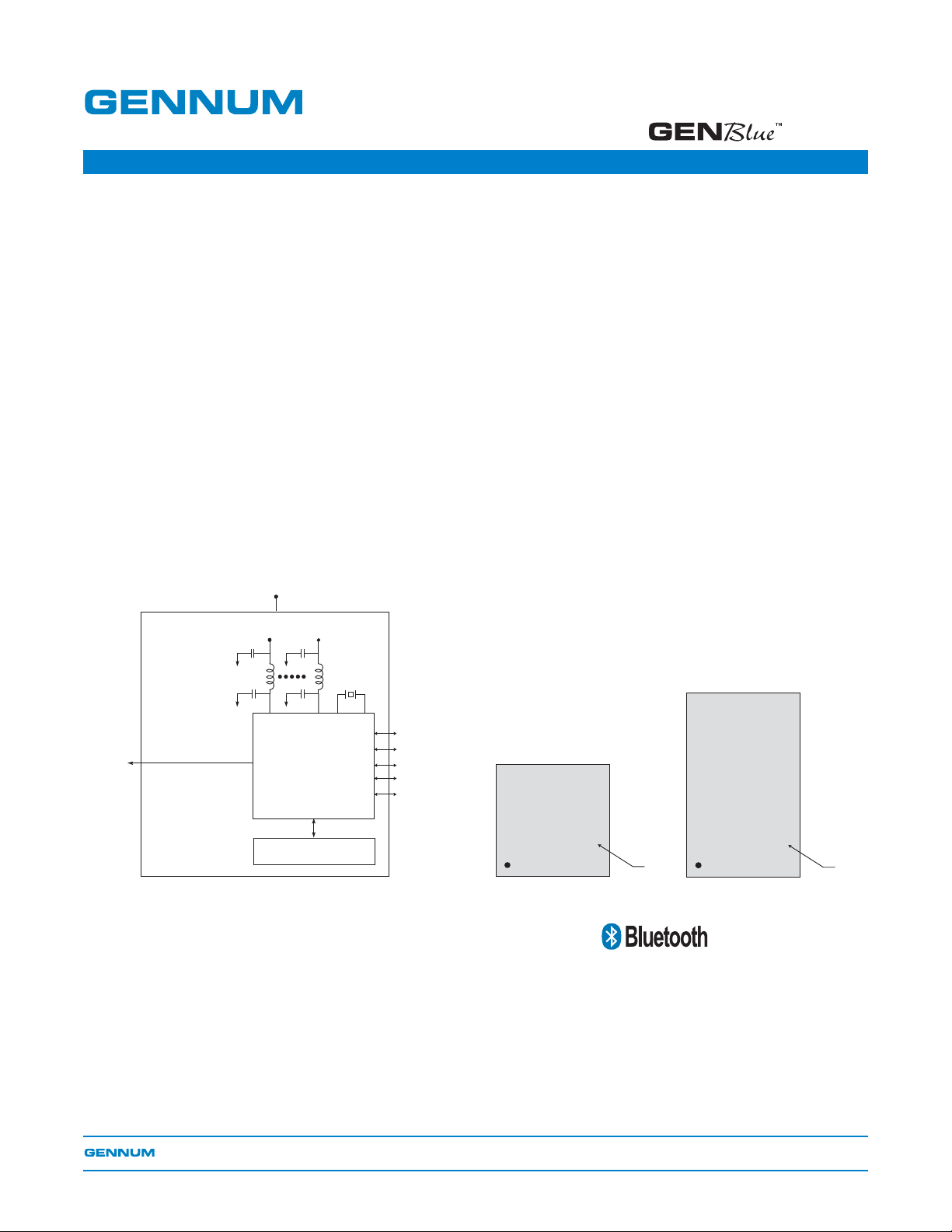
GR2316 / GR2320
Module
GR2316 / GR2320 Advance Information Note
Description
The GR2316 (without on-board antenna) / GR2320
(with on-board antenna) is one of the smallest modules
available providing the most flexibility for a wide range
of applications. Powered by Cambridge Silicon Radio’s
world leading single-chip technology, and combined
with Gennum’s packaging technology, the result is a
fully integrated module providing a complete system for
data and voice communications.
Applications
• Headsets
• Keyboards
• Mobile Phones
• Personal Digital Assistants (PDAs)
To Antenna
GR2316
Bluetooth™ is a trademark owned by the Bluetooth SIG, Inc. and licensed to Gennum Corporation.
BlueCore™ is a trademark owned by Cambridge Silicon Radio.
GenBlue™ is a trademark owned by Gennum Corporation.
+3V
Power Supply
Decoupling & Filtering
BlueCore ™ 2 - Flash
8 Mb
Flash
16 MHz
Crystal
Audio Input/Output
USB
UART
PCM
Programmable
Inputs/Outputs
Block diagram
GENNUM
FCC ID
SD7GR2316
XXXXXX
Lot No.
GENNUM
FCC ID
SD7GR2320
XXXXXX
Lot No.
®
Proprietary and Confidential 32197 - C April 2005 1 of 12
www.gennum.com
Page 2
1. Pinout
GR2316 / GR2320 Advance Information Note
Contents
Features ........................................................................................................................1
Description ....................................................................................................................1
Applications...................................................................................................................1
1. Pinout ........................................................................................................................2
2. Package Information .................................................................................................4
3. Pin Descriptions ........................................................................................................6
4. Typical Application ....................................................................................................9
5. FCC and EU Compliance........................................................................................10
6. Revision History ......................................................................................................12
SPI_MOSI
SPI_CLK
PCM_SYNC
PCM_OUT
PCM_IN
PCM_CLK
FLASH_EN
VDD_MEM0
VDD_CORE
VDD_MEM1
VDD_DIG
VDD_USB
UART_CTS
UART_RTS
SPI_MISO
A14 A13 A12 A11 A10
B14
C14
D14
E14
F14
G14
H14
J14
K14
L14
M14
N14
UART_RX
P14 P13 P12 P11 P10
SPI_CSB
UART_TX
GND
USB_DP
VDD_PADS
VDD_PIO
GND
A9 A8 A7 A6 A5 A4 A3 A2 A1
B10
D3
C10
C9 C8
D2D11
D9
D10
D10
E10
D12
F10
D14
G10
D7
USB_DN
D8D9
D1
D0
E9 E8
D4
D8
F8F9
D5
D6
G9 G8
D15
D13
CEXT
VREG_IN
P9 P8 P7 P6 P5 P4 P3 P2 P1
GND
AIO[1]
GND
AIO[0]
ANT
SPKR_P
GND
SPKR_N
GND
PIO[0]
GND
PIO[1]
PIO[11]
PIO[10]
B1
PIO[9]
C1
PIO[8]
D1
PI O[7]
E1
PIO[6]
F1
NC
G1
MIC_N
H1
MIC_P
J1
RESET
K1
PIO[5]
L1
PIO[4]
M1
PIO[3]
N1
PIO[2]
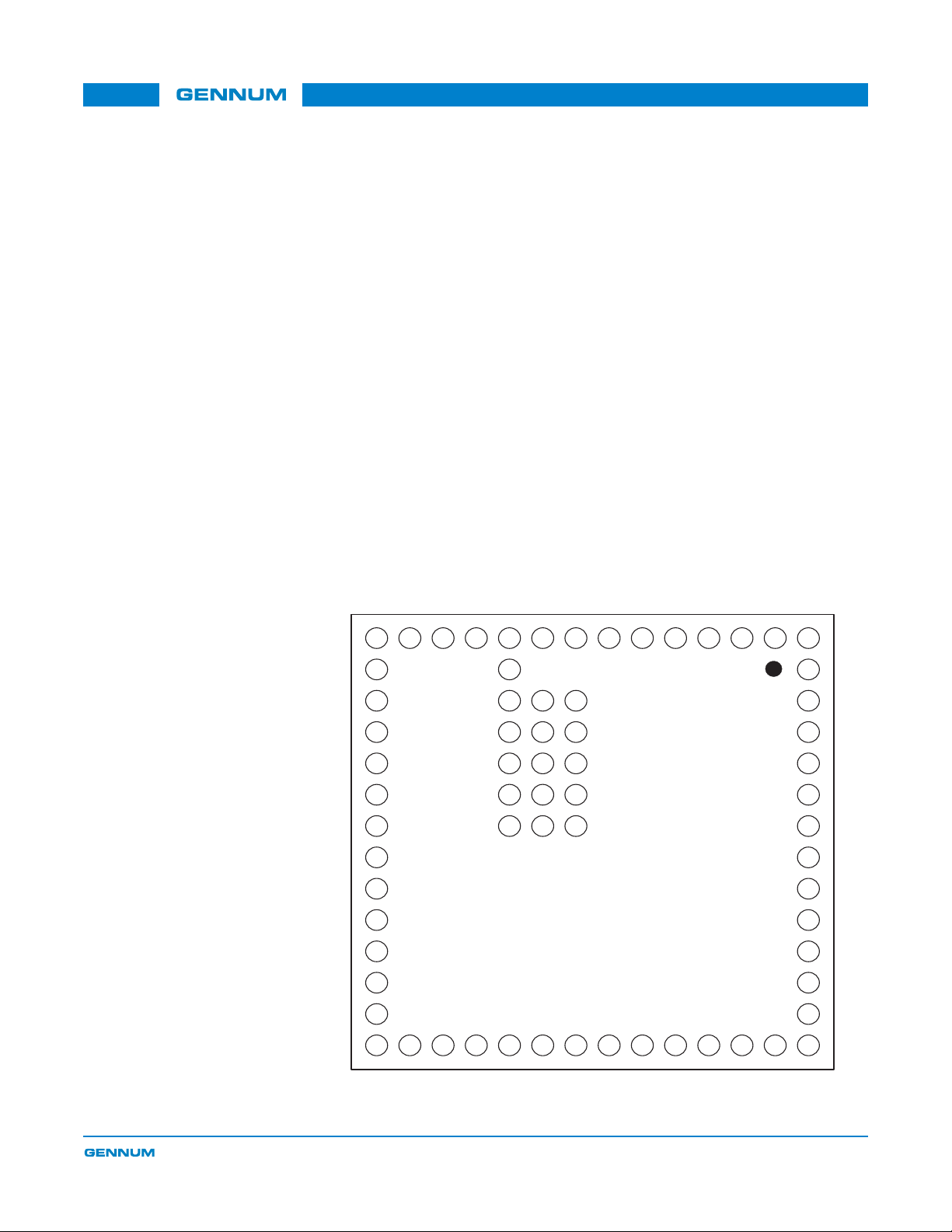
Figure 1-1: GR2316 bottom view
Proprietary and Confidential 32197 - C April 2005 2 of 12
Page 3
GR2316 / GR2320 Advance Information Note
GND
SPI_MOSI
SPI_CLK
PCM_SYNC
PCM_OUT
PCM_IN
PCM_CLK
FLASH_EN
VDD_MEM0
X0
X1
SPI_MISO
A14 A13 A12 A11 A10
B14
C14
D14
E14
F14
G14
H14
SPI_CSB
GND
VDD_PIO
VDD_PADS
B10
D3
C10
D10
D10
E10
D12
F10
D14
G10
D7
GND
A9 A8 A7 A6 A5 A4 A3 A2 A1
C9 C8
D2D11
D9
D8D9
D1
D0
E9 E8
D4
D8
F8F9
D5
D6
G9 G8
D15
D13
GND
GND
ANT
GND
GND
GND
X3
X2
GND
PIO[11]
PIO[10]
B1
PIO[9]
C1
PIO[8]
D1
PIO[7]
E1
PIO[6]
F1
NC
G1
MIC_N
H1
VDD_CORE
VDD_MEM1
VDD_DIG
VDD_USB
UART_CTS
UART_RTS
J14
K14
L14
M14
N14
P14 P13 P12 P11 P10
UART_RX
UART_TX
USB_DP
USB_DN
CEXT
VREG_IN
P9 P8 P7 P6 P5 P4 P3 P2 P1
AIO[1]
AIO[0]
SPKR_P
SPKR_N
PIO[0]
PIO[1]
MIC_P
J1
RESET
K1
PIO[5]
L1
PIO[4]
M1
PIO[3]
N1
PIO[2]
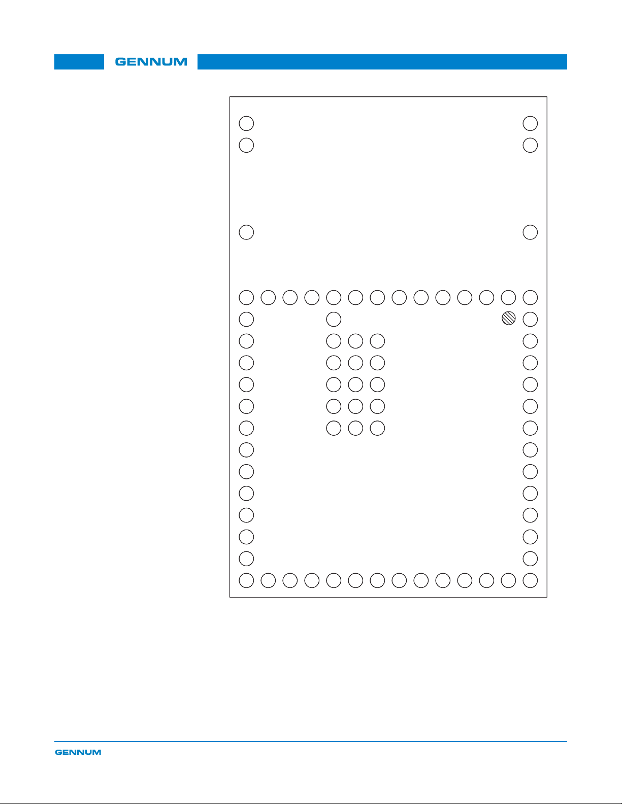
Figure 1-2: GR2320 bottom view
Proprietary and Confidential 32197 - C April 2005 3 of 12
Page 4
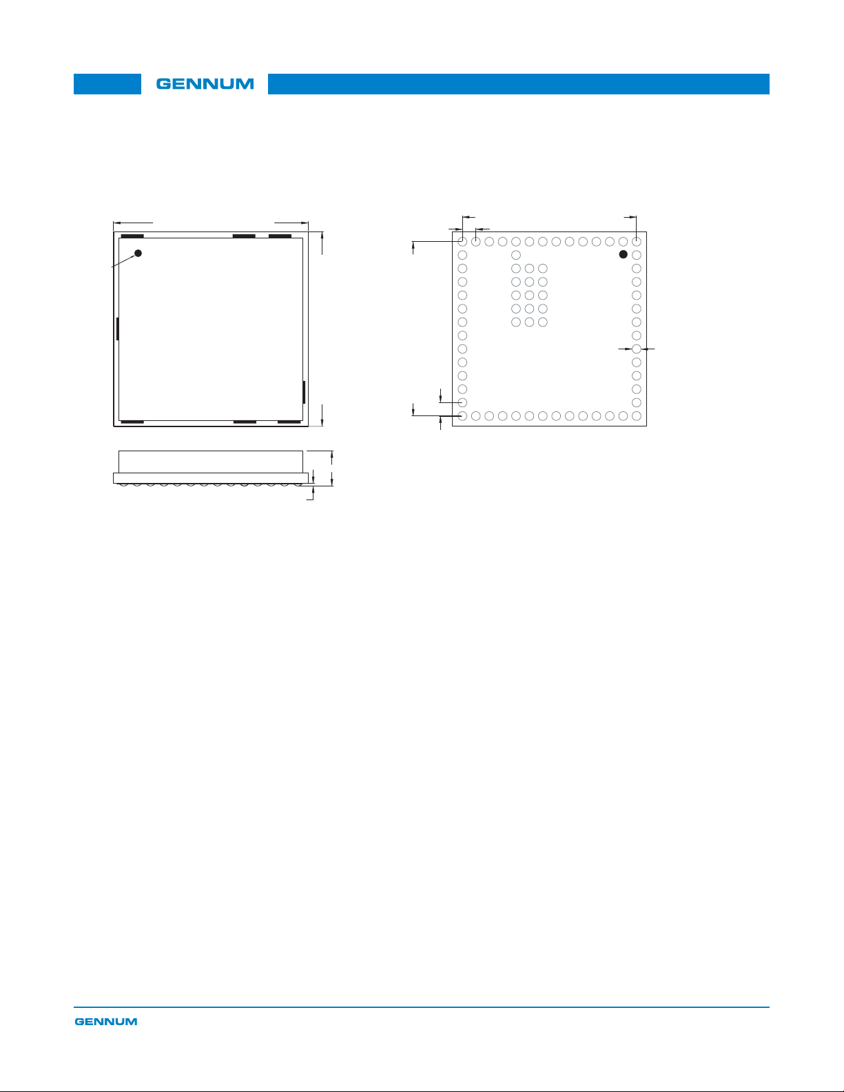
2. Package Information
GR2316 / GR2320 Advance Information Note
Index (A1)
0.5720"±0.0030" [14.530mm±0.08mm]
FCC ID
XXXXXX
SD7GR2316
TOP VIEW BOTTOM VIEW
SIDE VIEW
GENNUM
0.0080" [0.200mm]
0.5720"±0.0030" [14.530mm±0.08mm]
0.1200" [3.048mm] MAX
0.5118"±0.0030" [13.000mm±0.08mm]
0.0394" [1.000mm]
Figure 2-1: GR2316 package dimensions
NOTE: The following GigaAnt (www.gigaant.com) antennas have been approved
for use with the GR2316 module:
0.5118"±0.0030" [13.000mm±0.08mm]
0.0394" [1.000mm]
0.0260"±0.0010" [0.660mm±0.03mm]
•Rufa
•Picea
• Titanis
•Flavus
•Mica
For other types of antennas, please contact Gennum (bluetooth@gennum.com).
Proprietary and Confidential 32197 - C April 2005 4 of 12
Page 5

0.5720"±0.0030" [14.530mm±0.08mm]
GR2316 / GR2320 Advance Information Note
Index (A1)
C12
U3
R2
C11
FCC ID
XXXXXX
SD7GR2320
TOP VIEW BOTTOM VIEW
0.0040" [0.100mm] Z
SIDE VIEW
GENNUM
0.9050"±0.0030" [23.000mm±0.08mm]
0.0394" [1.000mm]
0.5118"±0.0030" [13.000mm±0.08mm]
0.1200" [3.048mm] MAX
0.0080" [0.200mm]
Figure 2-2: GR2320 package dimensions
0.5118"±0.0030" [13.000mm±0.08mm]
0.0394" [1.000mm]
0.0260"±0.0010" [0.660mm±0.03mm]
Proprietary and Confidential 32197 - C April 2005 5 of 12
Page 6

3. Pin Descriptions
Table 3-1: Pin Descriptions
GR2316 / GR2320 Advance Information Note
Pin
Number
A2 GND Ground connection to external low impedance ground plane
A3 GND Ground connection to external low impedance ground plane
A4 GND Ground connection to external low impedance ground plane
A6 GND Ground connection to external low impedance ground plane
A7 GND Ground connection to external low impedance ground plane
A8 GND Ground connection to external low impedance ground plane
A11 GND Ground connection to external low impedance ground plane
A5 (GR2316) ANT RF Connection to Antenna
A5 (GR2320) DNC Do not connect this pin for the GR2320
A12 SPI_CSB Chip select for serial peripheral interface, active low
A13 SPI_MISO Serial peripheral interface data output
A14 SPI_MOSI Serial peripheral interface data input
B14 SPI_CLK Serial peripheral interface clock
C14 PCM_SYNC Synchronous data sync
D14 PCM_OUT Synchronous data output
Pin
Name
Description
E14 PCM_IN Synchronous data input
F14 PCM_CLK Synchronous data clock
N14 UART_CTS UART clear to send, active low
P14 UART_RTS UART request to send, active low
P13 UART_RX UART data input, active low (idle status high)
P12 UART_TX UART data output, active low
P11 USB_P USB data plus with selectable internal 1.5k pull-up resistor
P10 USB_N USB data minus
P5 SPKR_P Speaker output positive
P4 SPKR_N Speaker output negative
J1 MIC_P Microphone input positive
H1 MIC_N Microphone input negative
P7 AIO(1) Programmable input/output line
P6 AIO(0) Programmable input/output line
Proprietary and Confidential 32197 - C April 2005 6 of 12
Page 7

GR2316 / GR2320 Advance Information Note
Table 3-1: Pin Descriptions (Continued)
Pin
Number
P3 PIO(0) Programmable input/output line
P2 PIO(1) Programmable input/output line
P1 PIO(2) Programmable input/output line
N1 PIO(3) Programmable input/output line
M1 PIO(4) Programmable input/output line
L1 PIO(5) Programmable input/output line
F1 PIO(6) Programmable input/output line
E1 PIO(7) Programmable input/output line
D1 PIO(8) Programmable input/output line
C1 PIO(9) Programmable input/output line
B1 PIO(10) Programmable input/output line
A1 PIO(11) Programmable input/output line
D8 D0 Extended input/output line
D9 D1 Extended input/output line
C9 D2 Extended input/output line
Pin
Name
Description
B10 D3 Extended input/output line
E9 D4 Extended input/output line
F8 D5 Extended input/output line
F9 D6 Extended input/output line
G10 D7 Extended input/output line
E8 D8 Extended input/output line
C8 D9 Extended input/output line
D10 D10 Extended input/output line
C10 D11 Extended input/output line
E10 D12 Extended input/output line
G8 D13 Extended input/output line
F10 D14 Extended input/output line
G9 D15 Extended input/output line
K1 RESET Reset high (input debounced so must be high for >5ms)
P8 CEXT Connection to external decoupling capacitor
G1 DNC No connection. Do not connect this pin.
P9 VREG_IN Linear regulator voltage input (3 VOLTS)
Proprietary and Confidential 32197 - C April 2005 7 of 12
Page 8

GR2316 / GR2320 Advance Information Note
Table 3-1: Pin Descriptions (Continued)
Pin
Number
A9 VDD_PIO Positive supply for PIO (connect to +3 volts supply)
A10 VDD_PADS Positive supply for digital input/output ports (connect to +3
M14 VDD_USB Positive supply for UART/USB ports (connect to +3 volts
L14 VDD_DIG Positive 1.8V supply output for VDD_MEM, FLASH_EN and
G14 FLASH_EN Connect to VDD_DIG
H14 VDD_MEM0 Connect to VDD_DIG
J14 VDD_CORE Connect to VDD_DIG
K14 VDD_MEM1 Connect to VDD_DIG
X0 (GR2320) – Mounting pad only
X1 (GR2320) – Mounting pad only
X2 (GR2320) – Mounting pad only
X3 (GR2320) – Mounting pad only
GND (GR2320) – Ground connection to external low impedance ground plane.
Pin
Name
Description
volts supply)
supply)
VDD_CORE
GND (GR2320) – Ground connection to external low impedance ground plane.
Proprietary and Confidential 32197 - C April 2005 8 of 12
Page 9

4. Typical Application
GR2316 / GR2320 Advance Information Note
SPI Interface
PCM Interface
2µ2
+3V Power Supply
UART Interface
{
{
{
SPI_MOSI
SPI_CLK
PCM_SYNC
PCM_OUT
PCM_IN
PCM_CLK
FLASH_EN
VDD_MEM0
VDD_CORE
VDD_MEM1
VDD_DIG
VDD_USB
UART_CTS
UART_RTS
Power Supply
SPI_MISO
A14 A13 A12 A11 A10
B14
C14
D14
E14
F14
G14
H14
J14
K14
L14
M14
N14
UART_RX
P14 P13 P12 P11 P10
SPI_CSB
UART_TX
GND
USB_DP
USB
Interface
+3V
VDD_PADS
VDD_PIO
A9 A8 A7 A6 A5 A4 A3 A2 A1
B10
D3
C9 C8
C10
D2D11
D10
D10
D1
E10
E9 E8
D12
D4
F10
D14
D6
G10
G9 G8
D15
D7
USB_DN
VREG_IN
P9 P8 P7 P6 P5 P4 P3 P2 P1
2µ2
{
GND
D9
D8D9
D0
D8
F8F9
D5
D13
CEXT
+3V
Power
Supply
GND
{
AIO[1]
2µ2
To
Antenna
GND
Extended I/O
AIO[0]
ANT
SPKR_P
GND
SPKR_N
Programmable
GND
PIO[0]
I/O
GND
PIO[1]
{
Speaker
PIO[11]
PIO[10]
B1
PIO[9]
C1
PIO[8]
D1
PIO[7]
E1
PIO[6]
F1
DNC
G1
MIC_N
H1
MIC_P
J1
RESET
K1
PIO[5]
L1
PIO[4]
M1
PIO[3]
N1
PIO[2]
{
Programmable
I/O
Microphone
To Bias Circuit
{
Programmable
I/O
Programmable
I/O
DNC = Do not connect, for test purposes only.
= Connection to low
impedance ground plane
Figure 4-1: Typical application circuit (bottom view)
Proprietary and Confidential 32197 - C April 2005 9 of 12
Page 10

+3V
GR2316 / GR2320 Advance Information Note
100K
2µ2
+
C
B
E
10µF
Figure 4-2: Typical Microphone Bias Circuit
5. FCC and EU Compliance
FCC Notice
This device complies with part 15 of the FCC Rules. Operation is subject to the
following two conditions:
1. This device may not cause harmful interference, and
1.1K
+
100ηF
MIC_P
MIC_N
2. This device must accept any interference received, including interference that
may cause undesired operation.
Changes or modifications not expressly approved by the party responsible for
compliance could void the user's authority to operate the equipment.
NOTE: This equipment has been tested and found to comply with the limits for a
Class B digital device, pursuant to part 15 of the FCC Rules. These limits are
designed to provide reasonable protection against harmful interference in a
residential installation. This equipment generates, uses and can radiate radio
frequency energy and, if not installed and used in accordance with the instructions,
may cause harmful interference to radio communications. However, there is no
guarantee that interference will not occur in a particular installation. If this
equipment does cause harmful interference to radio or television reception, which
can be determined by turning the equipment off and on, the user is encouraged to
try to correct the interference by one or more of the following measures:
• Reorient or relocate the receiving antenna
• Increase the separation between the equipment and receiver
• Consult the dealer or an experienced radio/TV technician for help
Proprietary and Confidential 32197 - C April 2005 10 of 12
Page 11

GR2316 / GR2320 Advance Information Note
If the modules are integrated in a way that they are not visible after installation, the
product in which the modules are integrated shall be labelled as follows:
• Contains FCC ID SD7GR2316
or
• Contains FCC ID SD7GR2320
EU Notice
In accordance with Annex IV of the EU directive 1999/5/EC,
Gennum Corporation
declares under our responsibility that the product:
Type:
GR2316 and GR2320
Intended Purpose: Bluetooth Transceivers
Equipment Class: 1
complies with the appropriate essential requirements of the Article 3 of the R&TTE
and the other relevant provisions, when used for its intended purpose.
Means of the efficient use of the radio frequency spectrum Art.3 (2)
EN 300 328-2 V1.2.1
, Electromagnetic compatibility and Radio Spectrum Matters
(ERM); Wideband Transmission systems; Data transmission equipment operating
in the 2.4 GHz ISM band and using spread spectrum modulation techniques;
Part 2: Harmonized EN covering essential requirements under article 3.2 of the
R&TTE Directive.
Proprietary and Confidential 32197 - C April 2005 11 of 12
Page 12

6. Revision History
Version ECR Date Changes and / or Modifications
A 134127 July 2004 New document.
B 134483 August 2004 Added features information, updated part marking,
C 136634 April 2005 Removed Note on page 1, added list of antennas,
GR2316 / GR2320 Advance Information Note
updated application schematic and added FCC and
EU notice.
added to FCC statement.
CAUTION
ELECTROSTATIC SENSITIVE DEVICES
DO NOT OPEN PACKAGES OR HANDLE
EXCEPT AT A STATIC-FREE WORKSTATION
DOCUMENT IDENTIFICATION
ADVANCE INFORMATION NOTE
The product is in a development phase and specifications are subject to
change without notice. Gennum reserves the right to remove the product
at any time. Listing the product does not constitute an offer for sale.
GENNUM CORPORATION
Mailing Address: P.O. Box 489, Stn. A, Burlington, Ontario, Canada L7R 3Y3
Shipping Address: 970 Fraser Drive, Burlington, Ontario, Canada L7L 5P5
Tel. +1 (905) 632-2996 Fax. +1 (905) 632-5946
GENNUM JAPAN CORPORATION
Shinjuku Green Tower Building 27F, 6-14-1, Nishi Shinjuku, Shinjuku-ku, Tokyo, 160-0023 Japan
Tel. +81 (03) 3349-5501, Fax. +81 (03) 3349-5505
GENNUM UK LIMITED
25 Long Garden Walk, Farnham, Surrey, England GU9 7HX
Tel. +44 (0)1252 747 000 Fax +44 (0)1252 726 523
Gennum Corporation assumes no liability for any errors or omissions in this document, or for the use of the
circuits or devices described herein. The sale of the circuit or device described herein does not imply any
patent license, and Gennum makes no representation that the circuit or device is free from patent infringement.
GENNUM and the G logo are registered trademarks of Gennum Corporation.
© Copyright 2004 Gennum Corporation. All rights reserved. Printed in Canada.
www.gennum.com
Proprietary and Confidential 32197 - C April 2005
12 of 12
12
 Loading...