

Page 1
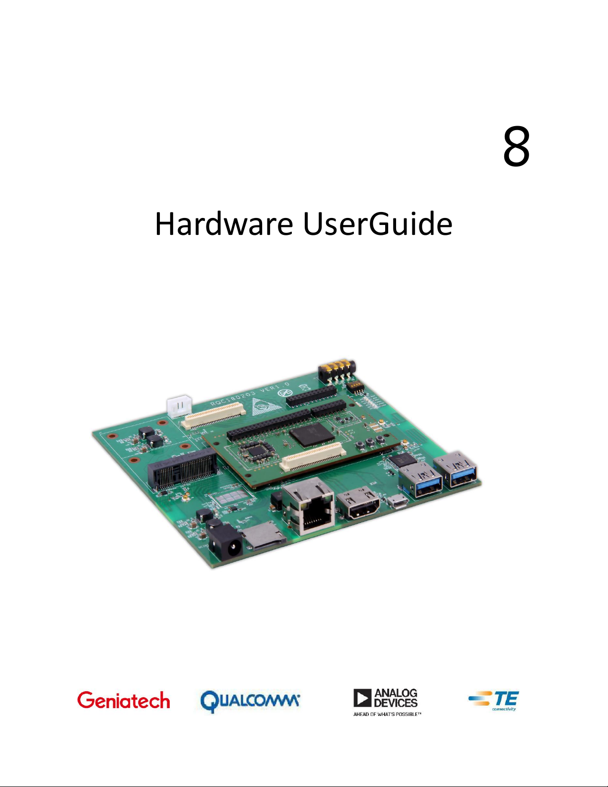
Developer Board 8
Powered by:
Hardware UserGuide
Page 2

2
Contents
1 Introduction
2 Key features........................................................................................................................................................................ 7
3 What’s in the Box..............................................................................................................................................................10
4 Getting started
4.1 Prerequisites
4.2 Starting the board for the first time
5 DragonBoard Overview.................................................................................................................................................... 13
5.1 System Block diagram............................................................................................................................................13
5.2 Processor............................................................................................................................................................... 13
5.3 Memory................................................................................................................................................................. 13
5.4 MicroSD................................................................................................................................................................. 14
........................................................................................................................................................................ 6
..................................................................................................................................................................12
.......................................................................................................................................................... 12
......................................................................................................................12
5.5 WiFi/BT/RF.............................................................................................................................................................14
5.6 Display Interface.................................................................................................................................................... 14
5.6.1 HDMI...........................................................................................................................................................14
5.6.2 MIPI-DSI......................................................................................................................................................14
5.7 Camera Interfaces
5.8 USB Ports
5.8.1 USB-Host ports...........................................................................................................................................15
5.8.2 USB-Device port......................................................................................................................................... 15
5.9 Audio......................................................................................................................................................................15
5.9.1 BT Audio
5.9.2 HDMI Audio
............................................................................................................................................................... 15
..................................................................................................................................................14
..................................................................................................................................................... 15
................................................................................................................................................15
Page 3

3
5.10 Input DC-power
5.11 Measurements.................................................................................................................................................... 16
5.12 Buttons................................................................................................................................................................ 16
...................................................................................................................................................16
5.13 UART
5.14 System and user LEDs
5.15 Expansion Connector
5.16 Additional Functionality......................................................................................................................................17
6 Low speed Expansion connector......................................................................................................................................18
6.1 UART {0/1}............................................................................................................................................................. 19
6.2 I2C {0/1}.................................................................................................................................................................19
6.3 GPIO {A-L}.............................................................................................................................................................. 20
.................................................................................................................................................................... 16
..........................................................................................................................................16
...........................................................................................................................................17
5.16.1 GPS............................................................................................................................................................17
5.16.2 Ethernet Connector..................................................................................................................................17
5.16.3 Mini PCIE connector................................................................................................................................. 17
6.4 SPI 0....................................................................................................................................................................... 20
6.5 PCM/I2S
6.6 Power and Reset
6.7 Power Supplies...................................................................................................................................................... 21
7 High speed expansion connectors....................................................................................................................................22
7.1 Primary high speed expansion connector.............................................................................................................22
7.1.1 MIPI DSI 0
7.1.2 MIPI CSI {0/1}
7.1.3 I2C {2/3}
................................................................................................................................................................. 20
....................................................................................................................................................20
................................................................................................................................................... 23
............................................................................................................................................. 24
......................................................................................................................................................24
Page 4

4
7.1.4 HSIC
7.1.5 Reserved..................................................................................................................................................... 24
7.1.6 SD/SPI......................................................................................................................................................... 24
.............................................................................................................................................................24
7.1.7 Clocks
7.1.8 USB
7.2 Secondary High Speed Connector
7.2.1 Feature information................................................................................................................................... 28
7.2.2 MIPI DSI 1................................................................................................................................................... 28
7.2.3 I2C {CCI_0,CCI _1, SSC_2}...........................................................................................................................28
7.2.3 SPI {SSC_1}..................................................................................................................................................28
7.2.4 TSIF – Transport Stream Interface..............................................................................................................28
7.2.5 Other signals on Secondary High Speed Connector.................................................................................. 28
8 Analog Expansion Connectors.......................................................................................................................................... 29
8.1 16-pin Analog Connector...................................................................................................................................... 29
..........................................................................................................................................................24
............................................................................................................................................................. 25
.........................................................................................................................25
8.1.1Earpiece.......................................................................................................................................................29
8.1.2 Microphones
8.1.3 Headset
9 24 pin Audio Expansion....................................................................................................................................................31
9.1 Analog Microphones............................................................................................................................................. 31
9.2 Digital Microphones.............................................................................................................................................. 32
9.3 Line Out
10 Power management
10.1 DC Power Input
................................................................................................................................................................. 32
.............................................................................................................................................. 29
.......................................................................................................................................................30
....................................................................................................................................................... 33
....................................................................................................................................................33
Page 5

5
10.2 Power Source Selection
10.3 Power Consumption............................................................................................................................................33
10.4 Power Sequencing...............................................................................................................................................33
.......................................................................................................................................33
11 Buttons and status LED’s
11.1 Buttons
11.1.1 Volume up
11.1.2 Volume down........................................................................................................................................... 35
11.1.3 Power Button............................................................................................................................................35
11.1.4 Entering Fastboot..................................................................................................................................... 35
11.1.5 Hard Reset................................................................................................................................................36
11.2 LEDs..................................................................................................................................................................... 36
11.2.1 User LED 1-4.............................................................................................................................................36
11.2.2 Bluetooth status....................................................................................................................................... 36
11.2.3 WiFi status................................................................................................................................................ 36
................................................................................................................................................................ 35
................................................................................................................................................ 35
................................................................................................................................................ 35
11.2.4 Power Indicator LED................................................................................................................................. 36
12 Boot configuration
13 Mechanical size marking
..........................................................................................................................................................37
................................................................................................................................................ 38
Page 6

6
1 Introduction
Acronym /
Abbreviation
Definition
BOM
Bill Of Materials
BT
Blue Tooth
CLK
Clock
CPU
Central Processing Unit
CS
Chip Select
CSI
Camera Serial Interface
DSI
Display Serial Interface
EMC
Electro-Magnetic Compatibility
EMI
Electro-Magnetic Interference
EN
ENable
ESD
Electro-Static Discharge
GND
GrouND
GPIO
General Purpose I/O
GPS
Global Positioning System
HDMI
High Definition Multimedia Interface
I2C
Inter-Integrated Circuit
I2S
Inter-IC Sound
INT
INTerrupt
ISP
Image Sensor Processor
LDO
Low Drop-Out
LRM
Linear Resonant Actuator
LTE
Long-Term Evolution
MDP
Mobile Display Port
MI2S
Mobile Inter-IC Sound
MIC
Microphone
MIPI
Mobile Industry Processor Interface
MPP
Multi-Purpose Pin
NFC
Near Field Communication
PCB
Printed Circuit Board
PCIE
Peripheral Component Interconnect Express
PWM
Pulse-Width Modulation
RF
Radio Frequency
RX
Receive
SCL
Serial CLock
SDA
Serial DAta
SDC
Secure Digital Interface
SOM
System On Module
SPI
Serial Peripheral Interface
SSC
Snapdragon™Sensor Core
TX
Transmit
UART
Universal Asynchronous Receiver/Transmitter
UIM
User Interface Module
USB
Universal Serial Bus
WLAN
Wireless Local Area Network
Acronyms and abbreviation definitions
Page 7
7
2 Key features
Processor
Qualcomm Snapdragon 820
Quad-core Qualcomm® Kryo™at up to 2.15GHz per core
64-Bit capable
Qualcomm® Adreno™530 624MHz GPU for PC-class graphics with support for advanced
APIs, including OpenGL ES 3.1+, OpenCL, DirectX, and content security
Memory/
Storage
3GB LPDDR4 1866MHz
32GB UFS 2.0
SD 3.0 (UHS-I)
Video
4K UltraHD@30fps video playback and capture with H.264 (AVC) and H.265 (HEVC)
Camera Support
Integrated Dual ISP with support for 3 image sensors up to 28MP
Audio
PCM/AAC+/MP3/WMA, ECNS, Audio+ post-processing (optional)
Connectivity
WLAN 2x2 802.11 b/g/n/ac 2.4 and 5GHz with on-board dual band WLAN antennas
Bluetooth v4.1 with on-board antenna
GbE Ethernet connection
One USB 2.0 micro B (device mode only)
Two USB 3.0 (host mode only)
GPS with On-board GPS antenna
I/O Interfaces
MINI PCIe
One 40-pin Low Speed (LS) expansion connector
• UARTx2, SPI, I2S, I2C x2, GPIO x12, DC power
Primary 60-pin High Speed (HS) expansion connector
• 4L-MIPI DSI, USB, I2C x2, 2L+4L-MIPI CSI, SPI
Secondary 60-pin High Speed (HS) expansion connector
• 4L-MIPI DSI, DC power, 1.8V supply, I2C, Camera Flash control, Display control,
2 x GPIO,Sensor core SPI, 3 x UART, I2C
Audio support including:
• Stereo Speaker and Mono microphone via 3.5mm headset jack
•24 pin audio expansion connector
•3.3V supply, 2 x analog line in, 4 x analog line out, speaker amp control, 2 x
digital microphone links supporting a total of 4 microphones
•16 pin audio expansion connector
•stereo headset/line out, speaker and analog line in
Camera connector based upon 96boards camera interface addendum. 30 pin connector
The Developer Board 8 (hereinafter referred to as DB8) board is a 96Boards compliant community board based on
Qualcomm® Snapdragon™ 820 processor.
The following table lists its key features:
Page 8
8
ZIF connector with 4L-CSI, DC power, 5V and 3.3V supply, camera control signals, I2C.
The DB8 board can be made compatible with Arduino compatible shield using an add-on
mezzanine. Go to:
http://www.96boards.org/product/sensors-mezzanine/
For more information about compatible mezzanine cards
External Storage
Micro SD card slot
User Interface
Switches
• Power/Reset
• Volume Up
• Volume down
6 LED indicators
• 4 - user controllable
• 2 - for radios (BT and WLAN activity)
OS-support
Linux Debian
Android
Power,
Mechanical and
Environmental
Input voltage: +6.5V to +18V
Dimensions: 100mm by 85mm meeting 96Boards™ Consumer Edition ’extended’
dimensions specifications.
Operating Temp: 0°C to +40°C
RoHS and Reach compliant
Page 9
9
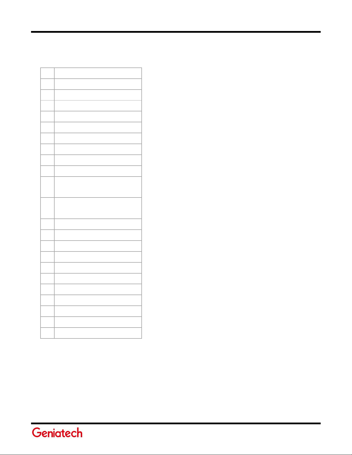
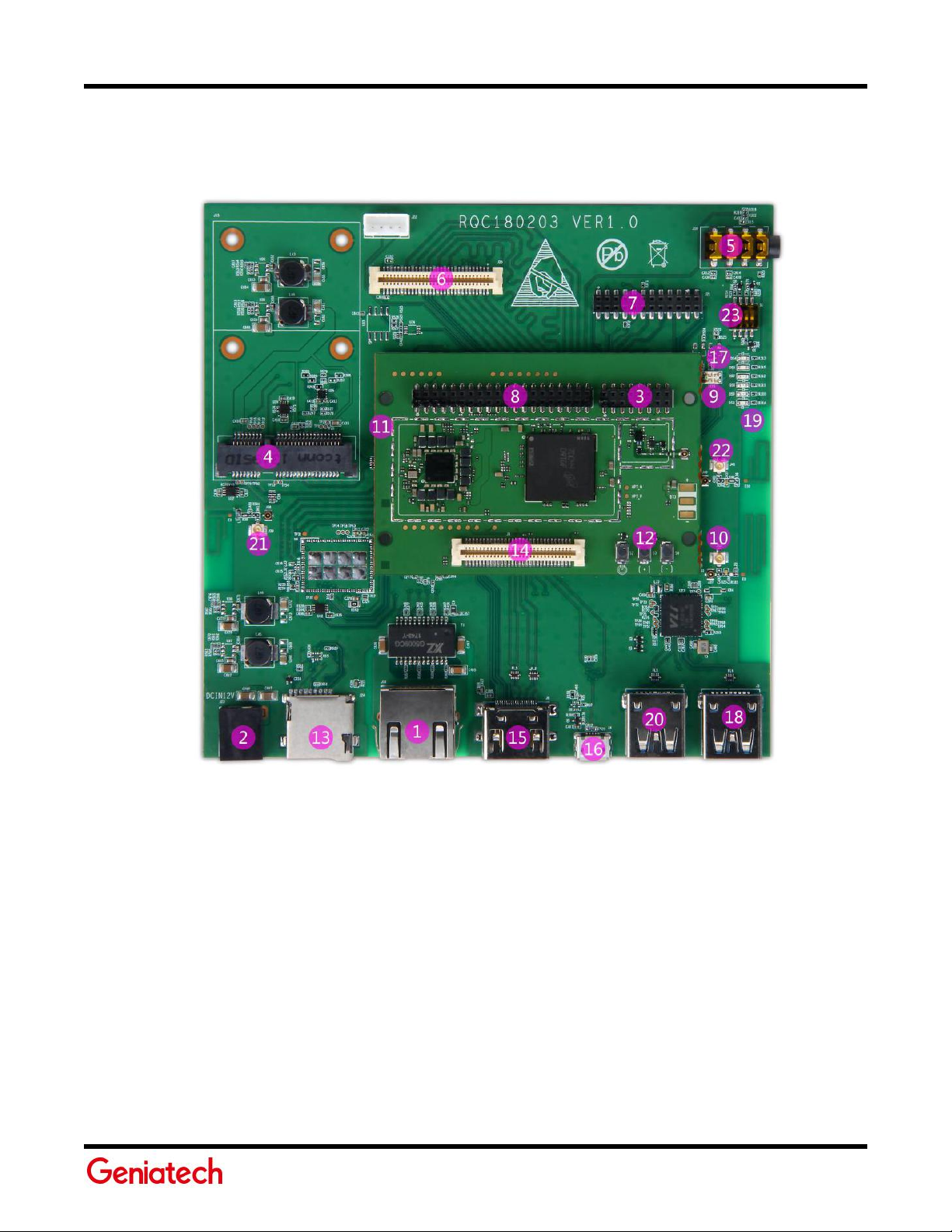
2.1 Board overview
1.
(J11) Ethernet Connector
2.
(J23) Power Jack
3.
(J7) Analog Expansion Connector
4.
(J15) MINI PCIE Connector
5.
(J16) 3.5mm Headset Jack
6.
(J20) Secondary High Speed Connector
7.
(J21) 24 pin Audio Connector
8.
(J8) Low Speed Connector
9.
(LED1) Power up indicator
10.
(GPS)GPS Antenna
11.
(SH1)Shield Compartment containing
APQ8096/LPDDR4, PM8996, WGR7640
12.
(S6) Power Button
(S5 S7) Vol+/Vol- Buttons
13.
(J24) microSD connector
14.
(J9) Primary High Speed Connector
15.
(J6)HDMI Connector
16.
(J4) Micro USB Type B Connector
17.
Bluetooth/WLAN LED’s
18.
(J3) USB Host1 connector
19.
User LEDs 1-4
20.
(J2) USB Host2 connector
21
(J38)WLAN/BT Antenna
22.
(J40)WLAN Antenna2
23.
(S1) Boot Switches
Page 10
10
Page 11
11
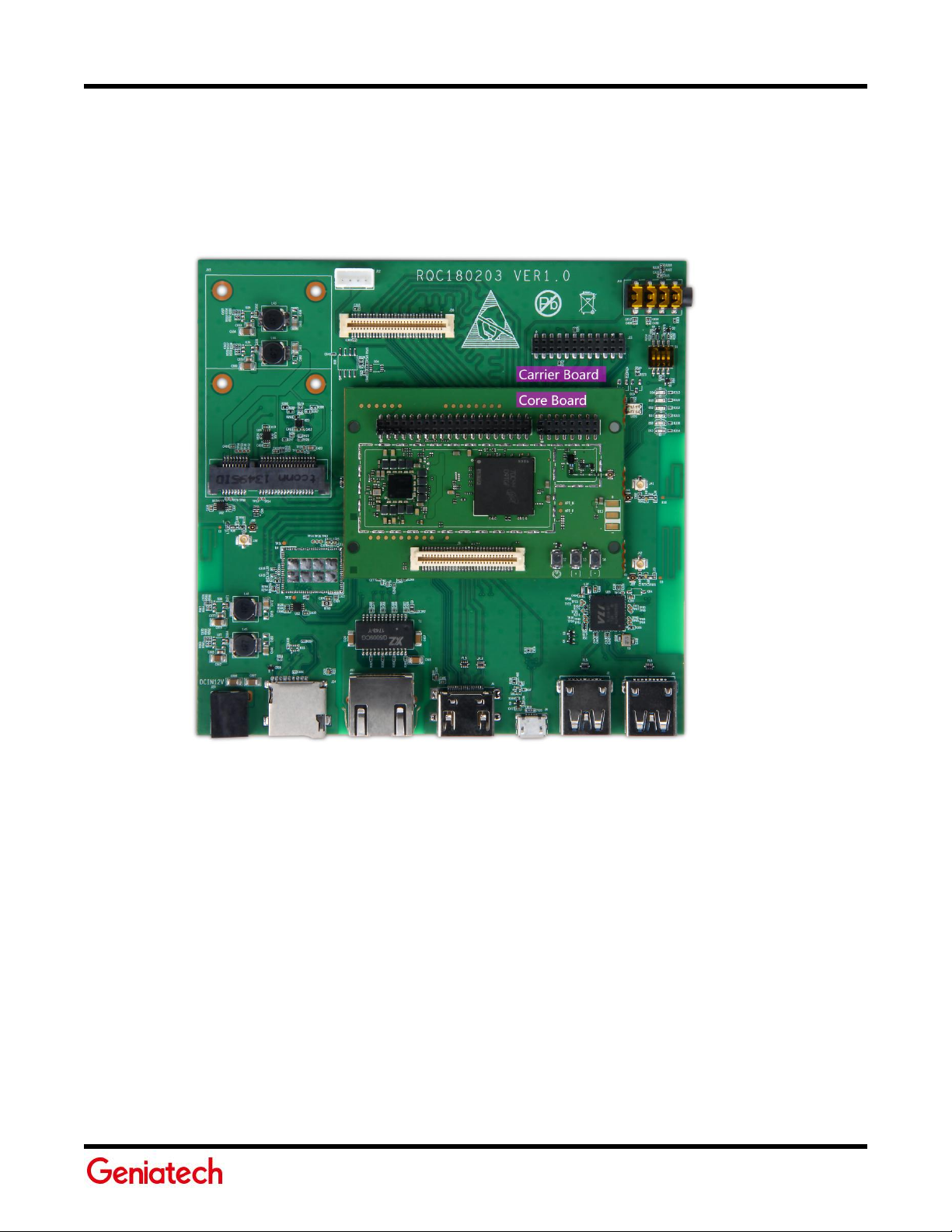
3 What’s in the Box
The box contains one DB8 development Core Board and one DB8 development Carrier Board.
Page 12

12
4 Getting started
● DB8 board
● A 96Boards compliant power supply (sold separately by Arrow) Input voltage range of 6.5-18V, recommended
● A HDMI or DVI LCD Monitor that supports a minimum resolution of 1080P/30Hz
● HDMI-HDMI cable or HDMI-DVI cable to connect the board to the Monitor
●
A computer keyboard with USB interface
● A computer mouse with USB interface
4.1 Prerequisites
Before you power up your DB8 for the first time you will need the following:
input current of 2A minimum.
4.2 Starting the board for the first time
To start the board, follow these simple steps:
step 1. Connect the HDMI cable to the DB8 HDMI connector (marked J6) and to the LCD Monitor.
step 2. Connect the mouse and keyboard to the DB8 USB connectors marked J2 and. (It doesn’t matter which order
you connect them in. You can also connect via an external USB Hub.)
step 3. Ensure that the boot switches S1 are set to ‘0000’, all in Off position.
step 4. Connect the power supply to power connector J23.
step 5.
The board will start the booting process, and you should see Linux or Android boot up. The ’power up’ Green LED
‘LED1’ should illuminate.
Please note that the first boot takes 3-4 minutes due to first time initialization. Subsequent boot times should be faster in
the range of 1-2 minutes.
Plug the power supply into a power outlet.
Page 13
13
5 DB8 Overview
●
The LPDDR4 interfaces directly to the APQ8096 built-in LPDDR controller. The maximum DDR clock is 1866 Mhz.
● The UFS flash memory interfaces with APQ8096 over a dedicated UFS/M-PHY bus supporting the UFS 2.0
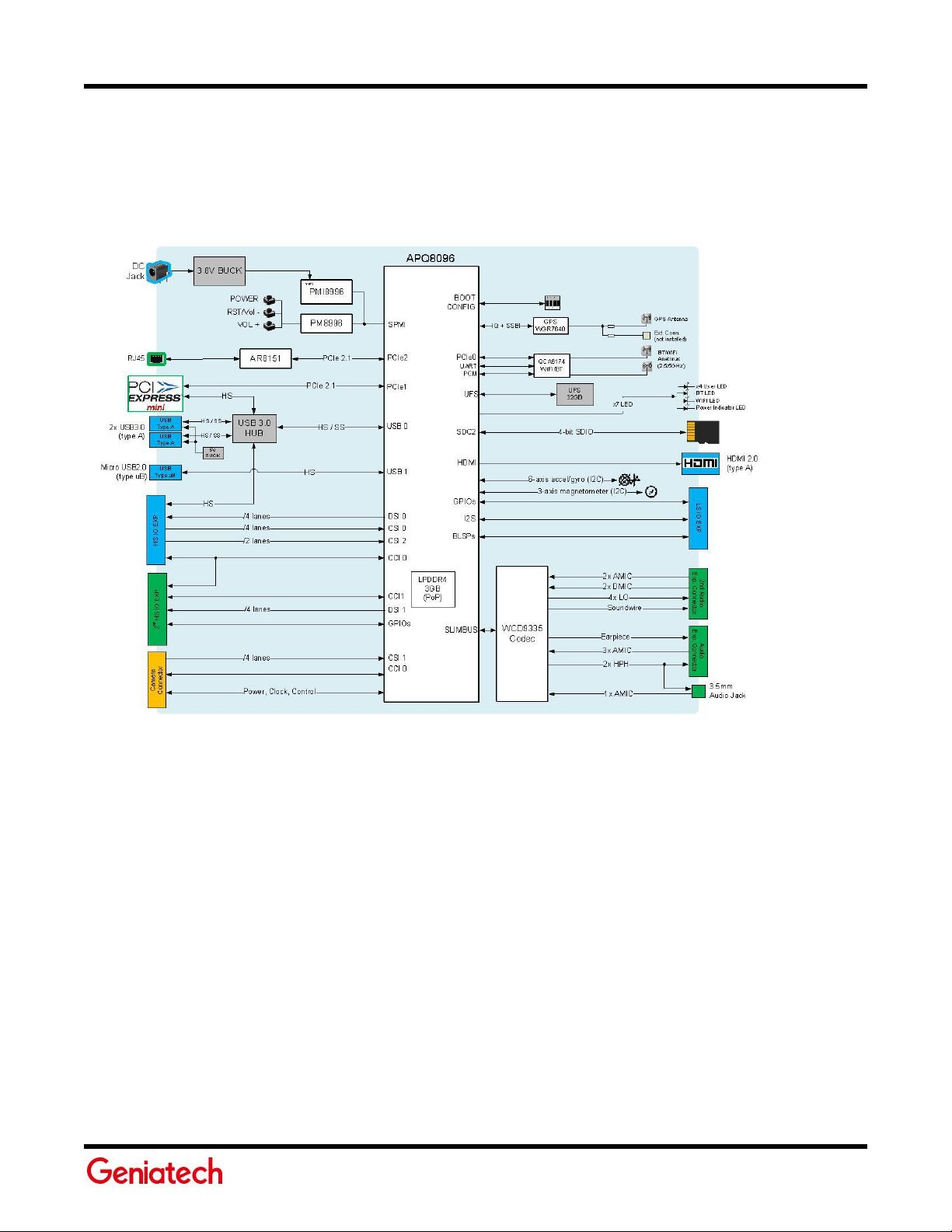
5.1 System Block diagram
5.2 Processor
The Snapdragon 820 (APQ8096) processor has a quad 64-bit Qualcomm® Kryo™ CPU,supporting LPDDR4 SDRAM
interface, Hexagon 680 DSP, 28 MP camera input support, Adreno 530 GPU, 4K Ultra HD video encode/decode,
gpsOneGen 8C with GLONASS, Bluetooth 4.1, OpenGL ES 3.1+, DirectX, OpenCL, Renderscript Compute, FlexRender
support.
5.3 Memory
The DB8 uses a package on package (PoP) LPDDR4 RAM configuration and discrete UFS 2.0 flash memory
specification.
Page 14

14
5.4 MicroSD
● 4 lane CSI camera on camera connector J20
● 4 lane CSI camera on primary high speed connector J9
●
2 lane CSI camera on primary high speed connector J9
The 96Boards specification calls for a microSD socket to be present on the board.
The DB8 µSD slot (J24) signals are routed directly to the APQ8096 SDC2 interface. The slot is a push-push type with a
dedicated support for card detect signal (many µSD slots do not have a dedicated CD pins, they use DATA3 state as the card
detected signal). The DB8 uses APQ GPIO_38 as the SD_CARD_DET_N.
5.5 WiFi/BT/RF
The 96Boards specifications calls for a WiFi (minimally 802.11g/n) and Bluetooth 4.1
The DB8 uses Qualcomm QCA6174A module solution that integrates two wireless connectivity technologies into a single
device, the interfaces are:
● WLAN compliant with IEEE 802.11 b/g/n/ac specifications, exceeding 96Boards minimal requirements for WiFi.
● Bluetooth compliant with the BT specifications version 4.1 (BR/EDR), meeting the 96Boards requirements for
BT.
5.6 Display Interface
5.6.1 HDMI
The 96Boards specification calls for an HDMI port to be on the board. The DB8 provides native support for an HDMI
interface. It supports a resolution up to 4K Ultra HD resolution at 60Hz.
5.6.2 MIPI-DSI
The 96Boards specification calls for a MIPI-DSI implementation via the High Speed Expansion Connector.
The DB8 implements a four-lane MIPI_DSI on the primary high speed connector interface which meets the 96boards MIPI-DSI high
speed connector requirement. An additional four-lane MIPI_DSI bus is implemented on the secondary high speed connector. More
information about this implementation can be found in chapter7 High speed expansion connector.
5.7 Camera Interfaces
The 96Boards specification calls for two camera interfaces.
The DB8 implements three camera interfaces.
Page 15

15
The DB8 includes an on-board 4-lane MIPI-CSI camera bus, routed to a 30 pin ZIF connector.
More information about this implementation can be found in chapter 7 High speed expansion connector.
5.8 USB Ports
5.8.1 USB-Host ports
The 96Boards specification calls for three USB host ports.
The DB8 supports 3 USB Host ports as follows.
Port 1 of the USB HUB is routed to J2, a Type ‘A’ USB Host 3.0 (Superspeed) connector. A current limited controller (U23)
sets the Power Current limit to 1.0A. This port is named HOST1 in the board schematic.
Port 2 of the USB HUB is routed to J3, a Type ‘A’ USB Host 3.0 (Superspeed) connector. A current limited controller (U23)
sets the Power Current limit to 1.0A. This port is named HOST2 in the board schematic.
Port 3 of the USB HUB is routed to the High Speed Expansion connector. No current limited controller is implemented on
the board for this channel.
5.8.2 USB-Device port
The 96Boards specification calls for a USB port to be implemented as an OTG port or a device port.
The DB8 implements a USB device port. The port is located at J4, a MicroUSB type B. If an application requires the use of
the device port, USB HUB_SEL switch (S1-4) shall be set to ‘0’ which is the default setting. Setting USB_SEL switch S1-4 to
‘ON’ will put the DB8 into Emergency Download mode (EDL) which will render the device
unusable for all other functionality.
5.9 Audio
The 96Boards specifications calls for a minimum of single channel audio through two interfaces, BT and
HDMI/MHL/DisplayPort.
The DB8 meets this requirement with HDMI support and has additional audio channels, including support for headset
jack. More information about these additional channels can be found in sections 8 and 9.
Note that MHL is not supported.
5.9.1 BT Audio
The BT 4.1 implementation on the DB8 is via a MAC in the APQ8096 and an external modem, contained in the WIFI/BT
module.
5.9.2 HDMI Audio
Page 16

16
HDMI audio is carried over the HDMI signals to the HDMI connector (J6).
● 8V to 18V input voltage power supplied from a dedicated DC jack
● 8V to 18V input voltage power supplied from the SYS_DCIN pins on the Low Speed Expansion Connector
• WiFi activity LED – DB8 drives this Yellow LED via MPP_2, an IO from the PMIC.
• BT activity LED – DB8 drives this Blue LED via MPP_4 an IO from the PMIC.
5.10 Input DC-power
The 96Boards specification calls for power to be provided to the board in one of the following ways:
Please see section 10 for detailed information on DB8 implementation of DC Power. Note that the DB8 does not
support USB Type C.
5.11 Measurements
The 96Boards specification calls for support for measuring power consumptions of the board.
Please see the power measurement section for detailed information on DB8 power measurement
implementation.
5.12 Buttons
The 96Boards specification calls for the presence of two buttons, a Power on/sleep button and a Reset button.
This board meets these requirements. Please see section 11 for detailed information on the buttons of the DB8.
5.13 UART
The 96Boards specification calls for support for one SoC UART and an optional second UART both to be routed to the Low
Speed Expansion Connector.
The DB8 routes 2 UARTs to the low speed connector.
5.14 System and user LEDs
The 96Boards specifications calls for six LEDs to be implemented on the board. The specification defines the LEDs color
and mechanical location on the board.
Two activity LEDs:
Four User-LEDs:
The four user LEDs are surface mount Green in 0603 size located next to the two USB type A connector and labeled ‘USER
Page 17

17
LEDS 3 2 1 0’. The DB8 drives three LEDs from the red, green and blue LED drive from power management IC PMI8996. The
fourth User LEDs is driven by the PMI8996 via PM MPP2.
Power indicator LED:
A blue LED is included to indicate the presence of input power to the DB8.
5.15 Expansion Connector
The 96Boards specification calls for two Expansion Connectors, a Low Speed and a High Speed.
The DB8 meets this requirement for low speed and exceeds it by having two high speed connectors, please review section
6 for detailed information regarding the Low Speed Expansion Connector and section 7 for detailed information regarding
the High Speed Expansion Connectors.
5.16 Additional Functionality
The 96Boards specifications allows for additional functionality provided that all mandatory functionality is available and
there is no impact on the physical footprint specifications including height and do not prevent the use of the 96Boards CE
low speed and high speed expansion facilities
The DB8 implements additional functions, which are listed in the following sub-chapters.
5.16.1 GPS
The GPS implementation is based on Qualcomm WGR7640 GNSS RF receiver (U5) supporting GPS, GLONASS and
COMPASS. The APQ8096 communicates directly with the WGR7640.
5.16.2 Ethernet Connector
Gigabit Ethernet is supported by Qualcomm AR8151 controller and uses an RJ45 as the physical interface.
5.16.3 Mini PCIE connector
The DB8 includes a mini PCIE (PCI express) connector. This enables integration of HW peripherals which are compliant to
the PCIE mini specification.
Page 18
18
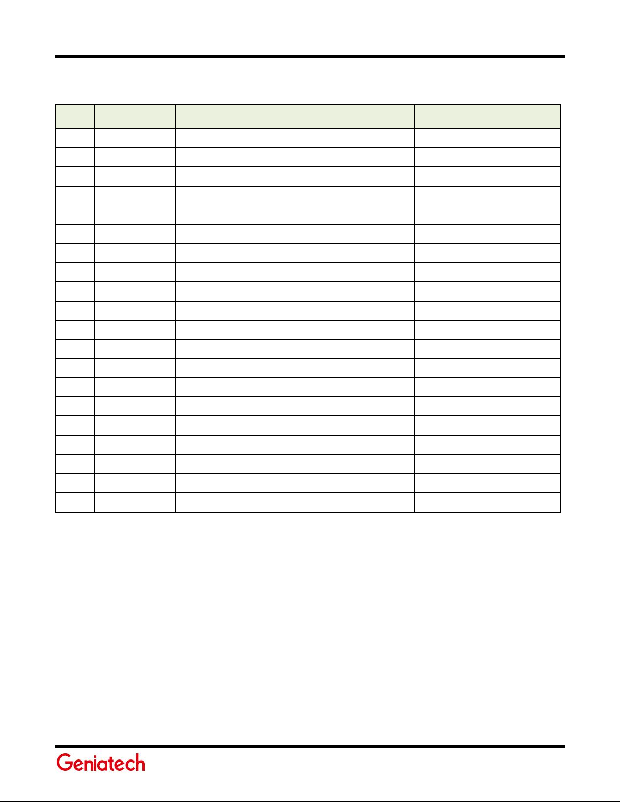
6 Low speed Expansion connector
PIN
96Boards Signals
DB8 Signals
Note
1
GND
GND
3
UART0_CTS
BLSP9_UART_CTS_N(APQ GPIO_51)
5
UART0_TxD
BLSP9_UART_TX (APQ GPIO_49)
7
UART0_RxD
BLSP9_UART_RX (APQ GPIO_50)
9
UART0_RTS
BLSP9_UART_RFR_N (APQ GPIO_52)
11
UART1_TxD
BLSP8_UART_TX(APQ GPIO_4)
13
UART1_RxD
BLSP8_UART_RX (APQ GPIO_5)
15
I2C0_SCL
BLSP3_I2C_SCL (APQ GPIO_48)
17
I2C0_SDA
BLSP3_I2C_SDA(APQ GPIO_47)
19
I2C1_SCL
BLSP8_I2C_SCL (APQ GPIO_7)
21
I2C1_SDA
BLSP8_I2C_SDA (APQ GPIO_6)
23
GPIO-A
MEMS_RESET_N (APQ GPIO_80)
25
GPIO-C
TS_INT0 (APQ GPIO_124)
27
GPIO-E
APQ_GPIO62 (APQ GPIO_62)
29
GPIO-G
MDP_VSYNC_P (APQ GPIO_10)
31
GPIO-I
CAM0_RST_N(APQ GPIO_25)
33
GPIO-K
CAM2_RST_N(APQ GPIO_23)
35
+1V8
VREG_S4A_1P8
37
+5V
VREG_5P0
39
GND
GND
The following tables show the Low Speed Expansion Connector pin out:
Page 19
19
PIN
96Boards
Signals
DB8 Signals
Note
2
GND
GND
4
PWR_BTN_N
BTN_PHONE_ON_N
6
RST_BTN_N
BTN_RESIN_N
8
SPI0_SCLK
BLSP1_SPI_CLK (APQ GPIO_3)
10
SPI0_DIN
BLSP1_SPI_MISO (APQ GPIO_1)
12
SPI0_CS
BLSP1_SPI_CS_N (APQ GPIO_2)
14
SPI0_DOUT
BLSP1_SPI_MOSI (APQ GPIO_0)
16
PCM_FS
QUA_MI2S_WS (APQ GPIO_59)
18
PCM_CLK
QUA_MI2S_SCK (APQ GPIO_58)
20
PCM_DO
QUA_MI2S_DATA0 (APQ GPIO_60)
22
PCM_DI
QUA_MI2S_DATA1 (APQ GPIO61)
24
GPIO-B
TS0_RESET_N (APQ GPIO_29)
26
GPIO-D
APQ_GPIO24 (APQ GPIO_24)
28
GPIO-F
BL0_PWM (PM_GPIO_5)
Used GPIO from PMIC
30
GPIO-H
LCD0_RESET_N (APQ GPIO_8)
32
GPIO-J
CAM0_STANDBY_N (APQ GPIO_26)
34
GPIO-L
CAM2_STANDBY_N (APQ GPIO_133)
36
SYS_DCIN
DC_IN
38
SYC_DCIN
DC_IN
40
GND
GND
6.1 UART {0/1}
The 96Boards specifications calls for a 4-wire UART implementation, UART0 and an optional second 2-wire UART, UART1
on the Low Speed Expansion Connector.
The DB8 implements UART0 as a 4-wire UART that connects directly to the APQ8096 SoC. These signals are driven at
1.8V.
The DB8 implements UART1 as a 2-wire UART that connects directly to the APQ8096 SoC. These signals are driven at
1.8V.
6.2 I2C {0/1}
Page 20

20
The 96Boards specification calls for two I2C interfaces to be implemented on the Low Speed Expansion Connector.
● Note: GPIO C - Connects to GPIO_125 of APQ8096 SoC, can serves as TS_INT0 supporting the
The DB8 implements both interfaces, I2C0 and I2C1 that connects directly to the APQ8096 SoC. A 2.2K resistor is
provided as pull-up for each of the I2C lines per the I2C specifications, these pull-ups are connected to the 1.8V voltage
rail.
6.3 GPIO {A-L}
The 96Boards specifications calls for 12 GPIO lines to be implemented on the Low Speed Expansion Connector. Some of
these GPIOs may support alternate functions for DSI/CSI control
The DB8 implements this requirement. 11 GPIOs are routed to the APQ8096 SoC and one GPIO is connected to the
on-board PMIC. All are 1.8V signals. Reference the connector pinout table for details regarding GPIO assignments
96Boards requirements to create a wake-up event for the SoC.
6.4 SPI 0
The 96Boards specification calls for one SPI bus master to be provided on the Low Speed Expansion Connector.
The DB8 implements a full SPI master with 4 wires, CLK, CS, MOSI and MISO all connect directly to the APQ8096 SoC.
These signals are driven at 1.8V.
6.5 PCM/I2S
The 96Boards specification calls for one PCM/I2S bus to be provided on the Low Speed Expansion Connector. The CLK, FS
and DO signals are required while the DI is optional.
The DB8 implements a PCM/I2S with 4 wires, CLK, FS, D0 and DI. The I2S signals are connected directly to the APQ8096
SoC. These signals are driven at 1.8V.
6.6 Power and Reset
The 96Boards specification calls for a signal on the Low Speed Expansion Connector that can power on/off the board and a
signal that serves as a board reset signal.
The DB8 routes the PWR_BTN_N (named PHONE_ON_N on DB8 schematic) signal to the KYPDPWR_N pin of the PMI8996
PMIC. This signal is driven by S2 as well, the on-board power on push-button switch. Please note that the push button only
provides an On/Sleep function and not OFF functionality.
A mezzanine implementation of this signals should not drive it with any voltage, the only allowed operation is to force it to
GND to start the board from a sleep mode. A board shutdown will occur when this signal is held to ground for more than
15 seconds.
Page 21

21
The DB8 routes the RST_BTN_N (named PM_RESIN_N on DB8 schematic) signal to the RESIN_N pin of the PMI8996 PMIC.
●
+1.8V
: Max of 100mA
● +5V: Able to provide a minimum of 5W of power (1A).
● SYS_DCIN : 9-18V input with enough current to support all the board functions or the output DCIN from
This signal is driven by S4, the on-board reset switch. This signals is a dual purpose, any press lasting less than 10 seconds
serves as Volume Down or Zoom out, a press longer than 10 seconds will reset the board.
6.7 Power Supplies
The 96Boards specification calls for three power rails to be present on the Low Speed Expansion Connector:
on-board DC Connector able to provide a minimum of 7W of power.
The DB8 supports these requirements as follows:
+1.8V
+5V : Driven by the 5A 5.0V DC to DC converter (on carrierboard-U37). This buck switcher powers both USB limit current
devices (each at 1.0A max). The remaining capacity provides a max current of 3A to the Low Speed Expansion Connector,
for a total of 8.2W which meets the 96Boards requirements.
SYS_DCIN: Can serves as the board’s main power source or can receive power from the board. It supports a minimum of
7W.
: Driven by PMIC LDO VREG_S4, which can provide 100mA.
Page 22
22
7 High speed expansion connectors
PIN
96Boards Signals
DB8 Signals
Note
1
SD_DAT0/SPI1_DOUT
BLSP12_SPI_MOSI (APQ GPIO_85)
This is a SPI implementation. not
an SD interface
No HSIC implementation
3
SD_DAT1
N.C.
5
SD_DAT2
N.C.
7
SD_DAT3/SPI1_CS
BLSP12_SPI_CS_N (APQ GPIO_87)
9
SD_SCLK/SPI1_SCLK
BLSP12_SPI_CLK (APQ GPIO_88)
11
SD_CMD/SPI1_DIN
BLSP12_SPI_MISO (APQ GPIO_86)
13
GND
GND
15
CLK0/CSI0_MCLK
CAM_MCLK0 (APQ GPIO_13)
17
CLK1/CSI1_MCLK
CAM_MCLK2 (APQ GPIO_15)
19
GND
GND
21
DSI_CLK+
MIPI_DSI0_CLK_P
23
DSI_CLK-
MIPI_DSI0_CLK_M
25
GND
GND
27
DSI_D0+
MIPI_DSI0_LANE0_P
29
DSI_D0-
MIPI_DSI0_CLK_M
31
GND
GND
33
DSI_D1+
MIPI_DSI0_LANE1_P
35
DSI_D1-
MIPI_DSI0_LANE1_M
37
GND
GND
39
DSI_D2+
MIPI_DSI0_LANE2_P
41
DSI_D2-
MIPI_DSI0_LANE2_M
43
GND
GND
45
DSI_D3+
MIPI_DSI0_LANE3_P
47
DSI_D3-
MIPI_DSI0_LANE3_M
49
GND
GND
51
USB_D+
USB_HS_D_P_EXP
53
USB_D-
USB_HS_D_M_EXP
55
GND
GND
57
HSIC_STR
N.C.
59
HSIC_DATA
N.C.
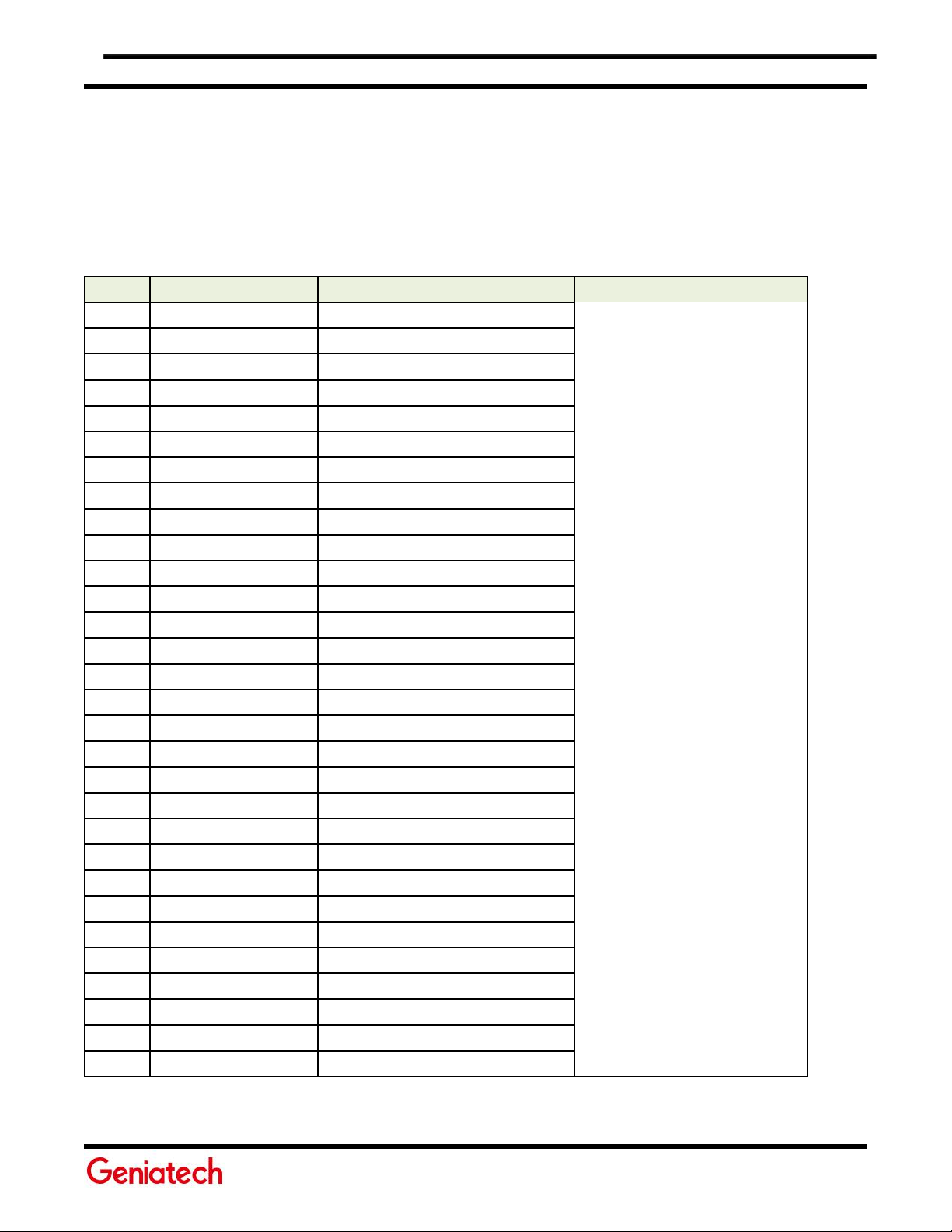
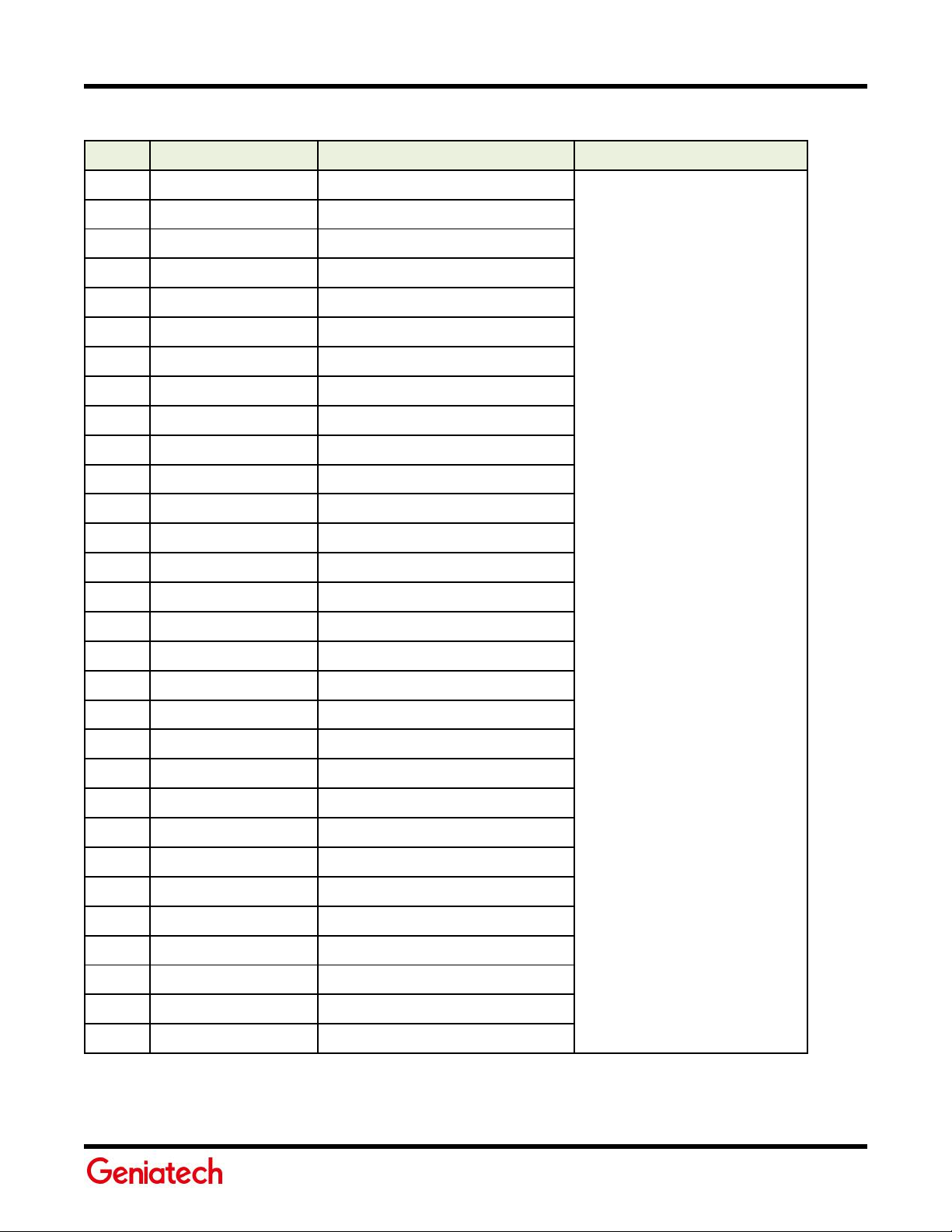
7.1 Primary high speed expansion connector
The following table shows the High Speed Expansion Connector pin out:
Page 23
23
PIN
96Boards Signals
820c Signals
Note
2
CSI0_C+
MIPI_CSI0_CLK_P
4
CSI0_C-
MIPI_CSI0_CLK_M
6
GND
GND
8
CSI0_D0+
MIPI_CSI0_LANE0_P
10
CSI0_D0-
MIPI_CSI0_LANE0_M
12
GND
GND
14
CSI0_D1+
MIPI_CSI0_LANE1_P
16
CCSI0_D1-
MIPI_CSI0_LANE1_M
18
GND
GND
20
CSI0_D2+
MIPI_CSI0_LANE2_P
22
CSI0_D2-
MIPI_CSI0_LANE2_M
24
GND
GND
26
CSI0_D3+
MIPI_CSI0_LANE3_P
28
CSI0_D3-
MIPI_CSI0_LANE3_M
30
GND
GND
32
I2C2_SCL
CCI_I2C_SCL0 (APQ GPIO_18)
34
I2C2_SDA
CCI_I2C_SDA0 (APQ GPIO_17)
36
I2C3_SCL
BLSP7_I2C_SCL (APQ GPIO_56)
38
I2C3_SDA
BLSP7_I2C_SDA (APQ GPIO_55)
40
GND
GND
42
CSI1_D0+
MIPI_CSI2_LANE0_P
44
CSI1_D0-
MIPI_CSI2_LANE0_M
46
GND
GND
48
CSI1_D1+
MIPI_CSI2_LANE1_P
50
CSI1_D1-
MIPI_CSI2_LANE1_M
52
GND
GND
54
CSI1_C+
MIPI_CSI2_CLK_P
56
CSI1_C-
MIPI_CSI2_CLK_M
58
GND
GND
60
RESERVED
VREG_S4A_1P8
Page 24

24
7.1.1 MIPI DSI 0
The 96Boards specification calls for a MIPI-DSI to be present on the High Speed Expansion Connector. A minimum of one
lane is required and up to four lanes can be accommodated on the connector.
The DB8 implementation supports a full four lane MIPI-DSI interface that is routed to the Primary High Speed
Expansion Connector.
7.1.2 MIPI CSI {0/1}
The 96Boards specification calls for two MIPI-CSI interfaces to be present on the High Speed Expansion Connector. Both
interfaces are optional. CSI0 interface can be up to four lanes while CSI1 is up to two lanes.
The current DB8 implementation supports a full four lane MIPI-CSI interface on CSI0 and two lanes of MIPI-CSI on
CSI2. All MIPI-CSI signals are routed directly to/from the APQ8096.
7.1.3 I2C {2/3}
The 96Boards specification calls for two I2C interfaces to be present on the High Speed Expansion Connector. Both interfaces
are optional unless a MIPI-CSI interface has been implemented. Then an I2C interface shall be implemented.
The current DB8 implementation supports two MIPI-CSI interfaces and therefore must support two I2C interfaces.
For MIPI-CSI0 the companion I2C2 is routed directly from the APQ8096. For MIPI-CSI2, the companion I2C is I2C3.
7.1.4 HSIC
The 96Boards specification calls for an optional MIPI-HSIC interface to be present on the High Speed Expansion Connector.
The DB8 implementation doesn’t support this optional requirement.
7.1.5 Reserved
The 96Boards specification calls for a 100K pull-up to 1.8V to be connected to pin 60 of the High Speed Expansion
Connector.
The DB8 utilizes a 100K pull-up (R147) on pin 60.
7.1.6 SD/SPI
The 96Boards specification calls for an SD interface or a SPI port to be part of the High Speed Expansion Connector.
The DB8 implements a full SPI master with 4 wires (96Boards SPI Configuration), CLK, CS, MOSI and MISO all connect
directly to the APQ8096 SoC. These signals are driven at 1.8V.
7.1.7 Clocks
The 96Boards specification calls for one or two programmable clock interfaces to be provided on the High Speed
Expansion Connector. These clocks may have a secondary function of being CSI0_MCLK and CSI1_MCLK. If these clocks
Page 25

25
can’t be supported by the SoC than an alternative GPIO or No-Connect is allowed by the specifications.
The DB8 implements two CSI clocks, CAM_MCLK0 via APQ GPIO_13 for CSI0 and CAM_MCLK2via APQ GPIO_15 for
CSI1. These signals are driven at 1.8V.
7.1.8 USB
The 96Boards specification calls for a USB Data line interface to be present on the High Speed Expansion Connector.
The DB8 implements this requirement by routing USB channel 3 from the USB HUB to the High Speed Expansion
Connector.
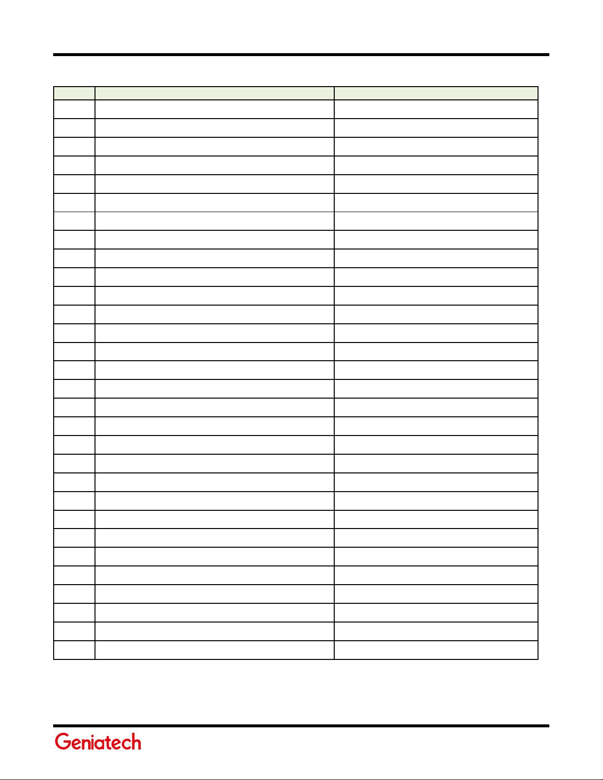
7.2 Secondary High Speed Connector
Given the extensive I/O available on the APQ8096, a second high speed connector(on carrierboard-J20) has been added
to support additional interfaces for development and integration.
Currently, the SW supporting these features is pre-commercial and many features are not implemented. Refer to the
notes section in the table regarding SW support.
While there are functions assigned for primary usages such as I2C bus, SPI bus, etc., most pins can be repurposed as
GPIOs if needed and their GPIO # assignments are included for reference. The following table shows the Secondary
High Speed Expansion Connector pin out:
Page 26
26
PIN
DB8 Signals
Note
1
SSC_SPI_1_MOSI(APQ SSC10)
Currently not configured in SW
3
NC
5
NC
7
SSC_SPI_1_CS_N (APQ SSC8)
Currently not configured in SW
9
SSC_SPI_1_CLK (APQ SSC9)
Currently not configured in SW
11
SSC_SPI_1_MISO(APQ SSC11)
Currently not configured in SW
13
GND
15
CAM_MCLK1(APQ-GPIO14)
17
NC
19
GND
21
MIPI_DSI1_CLK_P
23
MIPI_DSI1_CLK_M
25
GND
27
MIPI_DSI1_LANE0_P
29
MIPI_DSI1_LANE0_M
31
GND
33
MIPI_DSI1_LANE1_P
35
MIPI_DSI1_LANE1_M
37
GND
39
MIPI_DSI1_LANE2_P
41
MIPI_DSI1_LANE2_M
43
GND
45
MIPI_DSI1_LANE3_P
47
MIPI_DSI1_LANE3_M
49
GND
51
NC
53
NC
55
GND
57
DC_IN
59
DC_IN
Page 27
27
PIN
DB8 Signals
Note
2
MIPI_CSI1_CLK_P
4
MIPI_CSI1_CLK_M
6
GND
8
MIPI_CSI1_LANE0_P
10
MIPI_CSI1_LANE0_M
12
GND
14
MIPI_CSI1_LANE1_P
16
MIPI_CSI1_LANE1_M
18
GND
20
MIPI_CSI1_LANE2_P
22
MIPI_CSI1_LANE2_M
24
GND
26
MIPI_CSI1_LANE3_P
28
MIPI_CSI1_LANE3_M
30
GND
32
CCI_I2C_SCL0 (APQ GPIO_18)
34
CCI_I2C_SDA0 (APQ GPIO_17)
36
CCI_I2C_SCL1 (APQ GPIO_20)
38
CCI_I2C_SDA1 (APQ GPIO_19)
40
GND
42
NC
44
NC
46
NC
48
NC
50
GND
52
NC
54
NC
56
NC
58
NC
60
VREG_S4A_1P8
Page 28

28
7.2.1 Feature information
●
CCI_I2C_0
● CCI_I2C_1
●
1.8V supply
●
DC_IN 6.5V to 18V with up to 500mA maximum per pin on two pins
●
CAM_MCLK1(APQ-GPIO14)
Please refer to table notes column regarding which features are currently supported in SW.
7.2.2 MIPI DSI 1
The secondary high speed connector supports a 4-lane MIPI-DSI bus.
7.2.3 I2C {CCI_0,CCI _1, SSC_2}
The secondary high speed connector supports two I2C busses.
These busses can also be used as generic GPIOs.
7.2.3 SPI {SSC_1}
The secondary high speed connector supports one SPI bus- SSC_SPI_1.
This bus can also be used as generic GPIOs.
7.2.4 Other signals on Secondary High Speed Connector
Other signals include
Page 29
29
8 Analog Expansion Connectors
PIN
Function
Connect to
Note
1
CDC_EAR_M
2
CDC_EAR_P
3
VPH_PWR
4
GND
5
CDC_IN1_M
6
CDC_IN4_P
Mic 4 can be used for ANC
headset
7
CDC_IN1_P
8
CDC_HPH_R
9
HPH_REF
10
CDC_HPH_L
11
MBHC_HS_DET_L
Mechanical insertion detection
12
MIC_BIAS2
13
CDC_IN4_M
Mic 4 can be used for ANC
headset
14
CDC_IN3_M
Mic 3 can be used for ANC
headset
15
N.C.
16
CDC_IN3_P
Mic 3 can be used for ANC
headset
● CDC_EAR_M
●
CDC_EAR_P
● MIC1
● MIC3 Can be used as part of an active noise canceling (ANC) system
●
MIC4 Can be used as part of an active noise canceling (ANC) system
8.1 16-pin Analog Connector
Unless otherwise noted, these signals interface to the WCD9335 codec (U3).
8.1.1 Earpiece
The earpiece signals are routed from the WCD9335 codec, the two signals are:
8.1.2 Microphones
The 3 analog microphones are connected to the WCD9335 codec, the three mics are:
Page 30

30
● MIC_BIAS2 Ground reference
8.1.3 Headset
●
CDC_HPH_R
- Headphone PA right channel output
● CDC_HPH_L - Headphone PA left channel output
● HPH_REF - Headphone PA ground sensing
● MBHC_HS_DET_L - Headset detection
The headset signals are rounded from the WCD9335 codec, one signal is routed from the connector to the CODEC, the
singles are:
Page 31
31
9 24 pin Audio Expansion
PIN
Function
Connect to
Note
1
CDC_IN5_M
2
CDC_IN6_M
3
CDC_IN5_P
4
CDC_IN6_P
5
MIC_BIAS3
6
MIC_BIAS1
7
GND
8
SPKR_AMP_EN1
PMI8996 (U1)
9
CDC_SWR_CLK
10
CDC_SWR_DATA
11
SPKR_AMP_EN2
PMI8996 (U1)
12
GND
13
CDC_DMIC_CLK1
14
CDC_DMIC_CLK2
15
CDC_DMIC_DATA1
16
CDC_DMIC_DATA2
17
CDC_LINE_OUT2_M
18
CDC_LINE_OUT2_P
19
CDC_LINE_OUT1_M
20
CDC_LINE_OUT1_P
21
CDC_LINE_REF
22
VREG_3P3
3.3V from U20 buck switcher
23
CDC_LINE_OUT4
24
CDC_LINE_OUT3
●
MIC5
● MIC6
Unless otherwise noted, these signals interface to the WCD9335 codec (U3).
9.1 Analog Microphones
The 24 pin audio expansion connector supports 2 additional analog microphone inputs:
Page 32

32
● MIC_BIAS1, _BIAS3: Ground reference
9.2 Digital Microphones
●
DMIC_1
● DMIC_2
● Audio Amplifier interface. The 24 pin audio expansion connector supports the following interface and control of
● Amplifier control via SPKR_AMP_EN1, _EN2
The 24 pin audio expansion connector supports 2 additional analog microphone inputs:
9.3 Line Out
The 24 pin audio expansion connector supports 4 line outputs:
Line_Out1, Line_Out2: Differential drivenLine_Out3, Line_out4: Single ended with CDC_Line_Ref to use as a reference
ground.
audio amplifiers: Soundwire (CDC_SWR_CLK, SWR_DATA): Used and audio interface to Qualcomm WSA8810 or
8815 speaker amplifiers.
Page 33

33
10 Power management
●
An 8V to 18V power from a dedicated DC jack.
o The DB8 supports this requirement through the use of J23, ‘SYS_DCIN’ power connector. Please
●
Note that the DB8 operates from a ~24W supply such as a 12V/2A supply. An 8V to 18V power from the SYS_DCIN pins
The 96Boards specification defines how power arrives to the board and few supplies that the board needs to provide. The
on board power requirement for each 96Boards implementation depends on the SoC and the set of peripherals that are
specific to that implementation.
The DB8 uses three buck regulators,(carrierboard) U37, U38 and U35. U38 takes the power in to the board and generates
3.8V at 6A. This voltage serves as the power in voltage to the on-board PMI8996 IC. U37 takes the power in to the board
and generates 5V at 5A. This voltage feeds the USB HOST power limit switches, provides power to the Low Speed Expansion
port and other HW peripheral interfaces. U35 takes the power in to the board and generates 3.3V at 5A. 3.3V is used to
power HW peripherals as well as to expansion connectors.
10.1 DC Power Input
The 96Boards specification calls for a power to be provided to the board in one of the following ways:
note:the SYS_DCIN can be as low as 6.5V on the DB8.
on the Low Speed Expansion Connector.
Please note: the SYS_DCIN can be as low as 6.5V on the DB8. The DB8
supports incoming power through this connector.
10.2 Power Source Selection
Following the information in section 9.1, the DB8 has only two sources for board incoming power. The 96Boards
specification calls for only one power source to be applied to the board at any given time. Following this requirement,
the user of the DB8 should never apply power to the board from J1 and the Low Speed Expansion connector at the
same time.There is no active or passive mechanism on the DB8 to prioritize one source over the other.
10.3 Power Consumption
TBD
10.4 Power Sequencing
Upon applying power to the DB8 (either one of the two sources), both buck regulators will be enabled and will start
regulating their target voltages. When the output of U38 is on, it will power the on-board PMIC, the PMI8996. PMI8996
generates VPH_PWR which supplies the PM8996. The sequencing of all power rails is set within the PMIC configuration
Page 34

34
scheme during the production of this part. The user has no access to alter, modify or change the PMIC power up
sequencing.
Page 35
35
11 Buttons and status LED’s
●
You can put the device to sleep by pressing this button momentarily.
●
You can wake the device from sleep by pressing this button momentarily.
●
While the device is awake, pressing and holding the power button S6 for longer than 15 seconds will result in the
●
Once powered off, pressing and holding the power button S6 for longer than 15 seconds will result in the device
●
While the device is awake, pressing and holding the power button S6 for ~2-3 seconds seconds will result in the
●
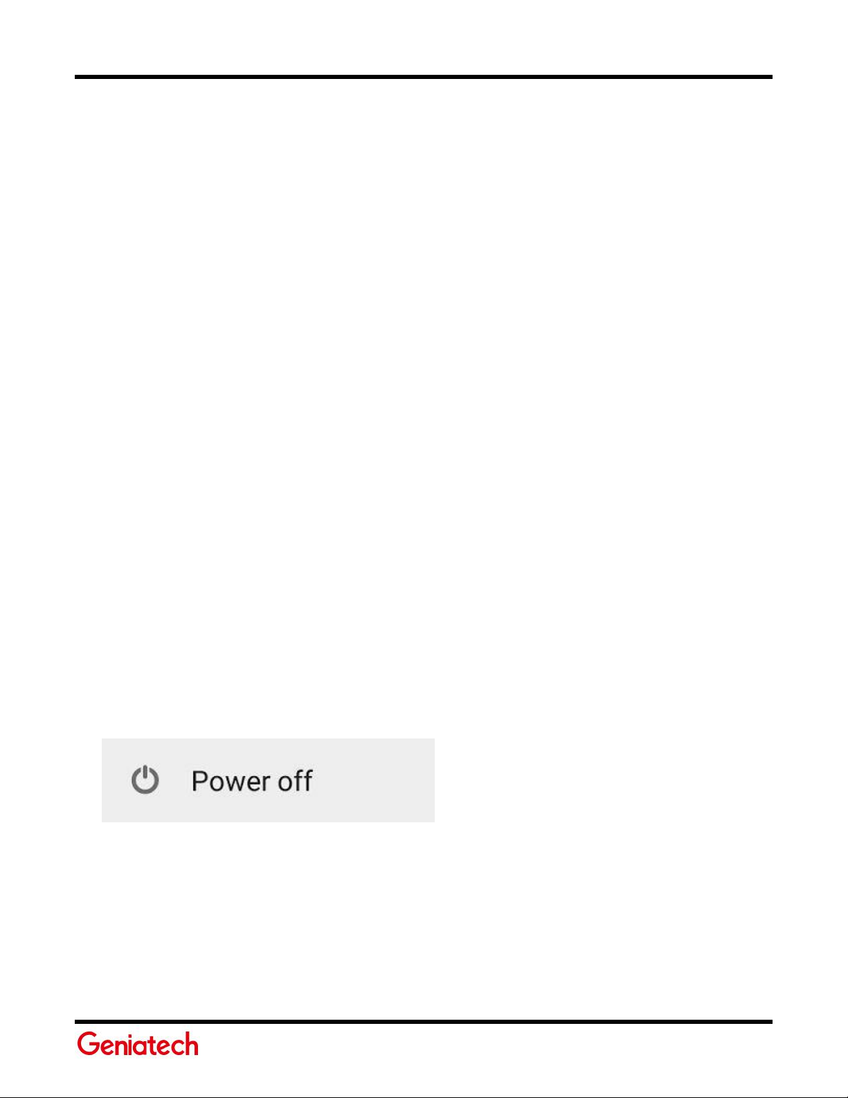
Using a mouse, clicking on this notifier will cause the DB8 to power off.
●
Once powered off, pressing and holding the power button S6 for longer than 2-3 seconds will result in the device
11.1 Buttons
11.1.1 Volume up
The Volume UP button (S5) is used to control the audio volume of the DB8.
11.1.2 Volume down
The Volume Down button (S7) is used to control the audio volume of the DB8.
11.1.3 Power Button
The push-button S6 serves as the power-on/off/sleep button. Upon applying power to the board, the boot process will
start. Once the board is powered on and booted up:
Sleep/suspend
Power Off/On
Option 1: Long press/hold
device powering off.
powering on.
user interface displaying the ‘power off’ notifier:
powering on.
11.1.4 Entering Fastboot
Holding down power and volume down buttons at power of the DB8 will force the device to enter fastboot mode.
Page 36

36
11.1.5 Hard Reset
Holding power and volume down buttons for 15 seconds will force a hard reset of the DB8.
11.2 LEDs
There are two status LEDs and four User LEDs on the DB8. The Status LEDs report the status of the Bluetooth and
Wi-Fi devices onboard. The user LEDs are driven by the SoC directly.
11.2.1 User LED 1-4
The four user LEDs are surface mount Green LEDs, 0603 size, labeled ‘DS2 DS1 DS0 DS3’.
11.2.2 Bluetooth status
The BT LED on the carrierboard is located beside the WIFI LED; this LED reflects the status of the Bluetooth device.
11.2.3 WiFi status
The WIFI LED on the carrierboard is located next to the S1, this LED reflects the status of the Wi-Fi device.
11.2.4 Power Indicator LED
The DB8 contains a power indicato(carrierboard-LED1) to notify the user that power is applied.
Page 37
37
12 Boot configuration
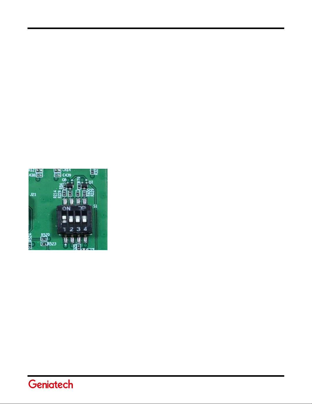
There is a 4 switch Dip Switch marked S1 located at the carrierboard. For normal operation, all four switches need to be
set to the ‘off’ position.
Switch 1, ‘HUB_SEL’, when set to ‘on’ position, will force boot over USB connection with a PC. This is only required for
UFS boot image upgrade. Please review the proper OS User Guide for more information on this process.
Switch 2, SD BOOT’, when set to ‘on’ position, will force the µSD, J24, to serve as the boot source for the DB8. You can use
uSD as the main boot source or it can serve as a method for UFS boot image upgrade. Please review the proper OS User
Guide for more information on this process.
Switch 3, ‘SW Download Target Memory’, when set to ‘on’ position, will force SW download/flashing to the µSD card, J24
When set to ‘off’ position, SW download will route to the UFS memory.
Switch 4, ‘USB BOOT’, when set to ‘on’ position, selects USB Port 0 for EDL download mode. Please review the proper OS
User Guide for more information on this process.
Page 38
38
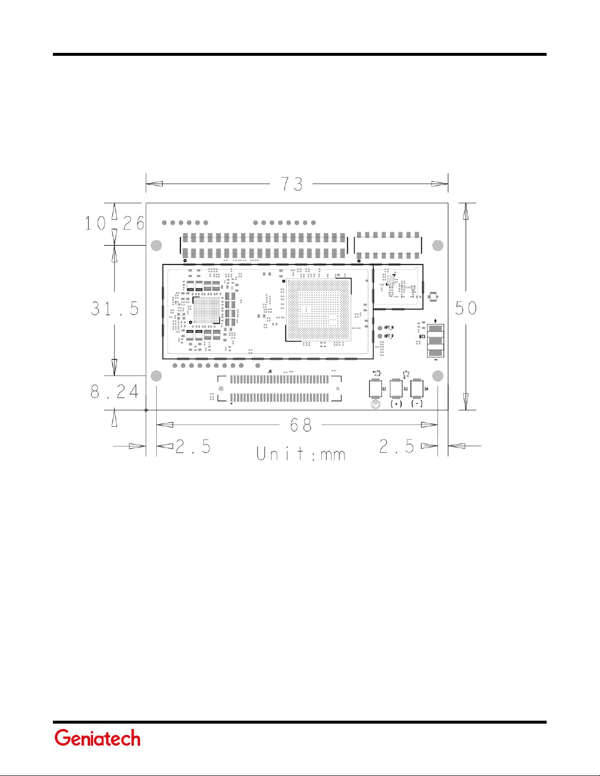
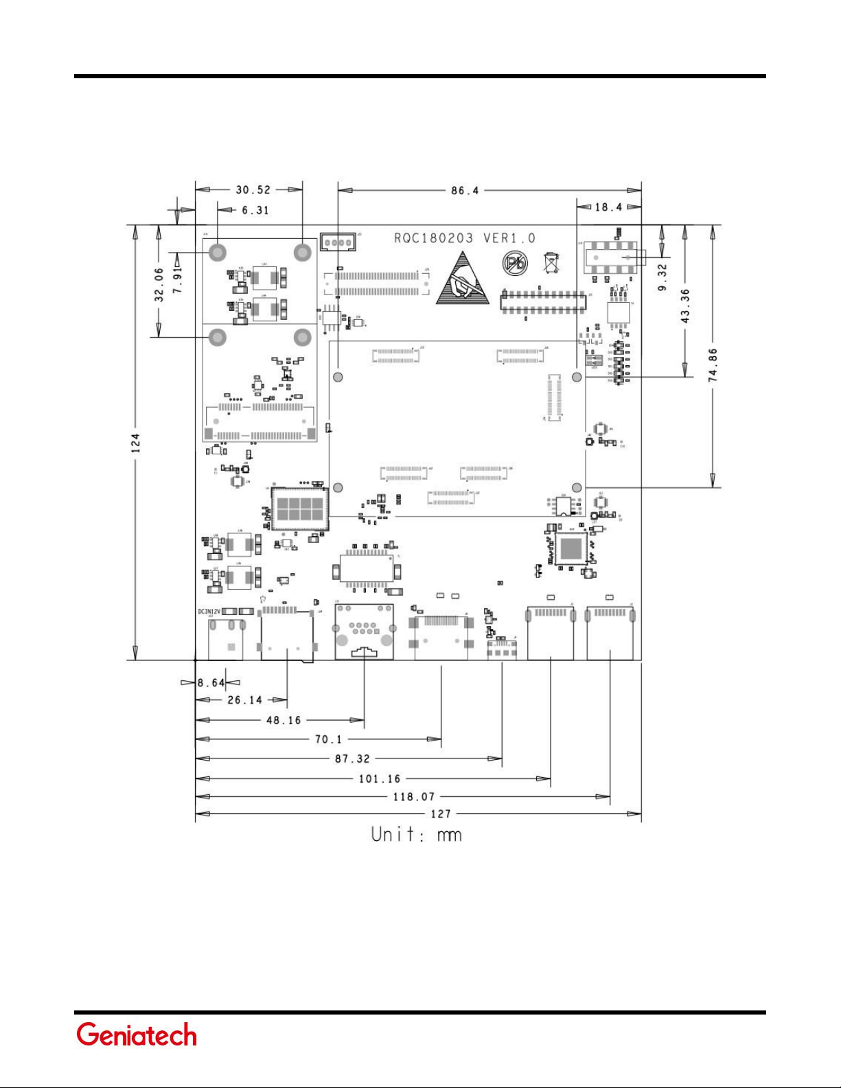
13 Mechanical size marking
Page 39

FCC warning
This equipment has been tested and found to comply with the limits for a Class B digital device, pursuant to part 15 of the FCC
Rules. These limits are designed to provide reasonable protection against harmful interference in a residential
installation. This equipment generates, uses and can radiate radio frequency energy and, if not installed and used in
accordance with the instructions, may cause harmful interference to radio communications. However, there is no
guarantee that interference will not occur in a particular installation. If this equipment does cause harmful interference to
radio or television reception, which can be determined by turning the equipment off and on, the user is encouraged to try to
correct the interference by one or more of the following measures:
- —Reorient or relocate the receiving antenna.
- —Increase the separation between the equipment and receiver.
- —Connect the equipment into an outlet on a circuit different from that to which the receiver is connected.
- —Consult the dealer or an experienced radio/TV technician for help.
This device complies with part 15 of the FCC Rules. Operation is subject to the following two conditions: (1) This device may not
cause harmful interference, and (2) this device must accept any interference received, including interference that may cause
undesired operation.
You are cautioned that changes or modifications not expressly approved by the party responsible for compliance could void
your authority to operate the equipment.
The distance between user and products should be no less than 20cm
Page 40
39
 Loading...