

Genesis gm5120H, gm5120, gm5110H, gm5110 Datasheet

Genesis Microchip Inc.
2150 Gold Street, Alviso, P.O. Box 2150, CA USA 95002 Tel: (408) 262-6599 Fax: (408) 262-6365
165 Commerce Valley Dr. West, Thornhill, ON Canada L3T 7V8 Tel: (905) 889-5400 Fax: (905) 889-5422
1096, 12thA Main, Hal II Stage, Indira Nagar, Bangalore-560 008, India, Tel: (91)-80-526-3878, Fax: (91)-80-529-6245
4F, No. 24, Ln 123, Sec 6, Min-Chuan E. Rd., Taipei, Taiwan, ROC Tel: 886-2-2791-0118 Fax: 886-2-2791-0196
143-37 Hyundai Tower, #902, Samsung-dong, Kangnam-gu, Seoul, Korea 135-090 Tel 82-2-553-5693 Fax 82-2-552-4942
Rm2614-2618 Shenzhen Office Tower, 6007 Shennan Blvd, 518040, Shenzhen, Guandong, P.R.C., Tel (0755)386-0101, Fax (0755)386-7874
2-9-5 Higashigotanda, Shinagawa-ku, Tokyo, 141-0022, Japan, Tel 81-3-5798-2758, Fax 81-3-5798-2759
www.genesis-microchip.com / info@genesis-microchip.com
Genesis Microchip Publication
PRELIMINARY DATA SHEET
gm5110/gm5110-H
gm5120/gm5120-H
XGA/SXGA LCD Controller
*** Genesis Microchip Confidential ***
NOTE: Sections in this data sheet that mention HDCP apply only to the HDCP-enabled chip
versions (gm5110-H and gm5120-H). All other sections apply to all chip versions (gm5110,
gm5110-H, gm5120, and gm5120-H).
Publication number: C5110-DAT-01C
Publication date: June 2002
*** Genesis Microchip Confidential *** gm5110/20 Preliminary Data Sheet
Revision History
Document Description Date
C5110-DAT-01A
• Initial release
Aug 2001
C5110-DAT-01B
• Added note on Front Cover regarding HDCP enabled versions.
• Added section 4.12 - Energy Spectrum Management (ESM).
• In section 4.15 clarified that ROM_ADDR[15:0] have internal 60KΩ pull-down
resistor.
• Changes to Table 21– DC Characteristics:
– Renamed parameters θ
JA_XGA
, θ
JA_SXGA
, θ
JC_XGA
and θ
JC_SXGA
to θ
JA_5110
, θ
JA_5120
,
θ
JC_5110
and θ
JC_5120
and revised their values.
– Added note (4) regarding the maximum case temperature.
• Changes to Table 22– Maximum Speed of Operation:
– Renamed parameters P
5110
and P
5120
and revised their values.
– Renamed parameters I
5110
, I
5110_2.5_VDD
, etc.
– Added note (6).
• Removed the clock speed column from section 6 - Ordering Information and
added the ordering information for gm5110-H and gm5120-H.
Oct 2001
D5110-DAT-01C
• Pins 143 ~ 146: changed xxx_SDDS or xxxx_SDDS to xxx_DDDS or xxxx_DDDS
respectively
• Pins 138 ~ 141: changed xxx_DDDS or xxxx_DDDS to xxx_SDDS or xxxx_SDDS
respectively
• Pins 147 ~ 148: changed xxx_DPLL to xxx_RPLL
June
2002
Related documents
Chip documents
C5110-PBR-01 Preliminary Product Brief gm5110
C5120-PBR-01 Preliminary Product Brief gm5120
C5115-APB-01 gm5115 Product Family On-chip Microcontroller (OCM) Firmware Configurations
C5115-APB-02 gm5115 Product Family Support for Standard RGB (sRGB)
C5115-TOP-01 gm5115 Theory of Operation
C5115-DSL-01 gm5115 Register Listing
C5115-DSR-02 gm5115 Input Processing Programming Guide
Reference design documents
B0108-GUD-01 5110RD1 Reference Design Users Guide
B0108-SCH-01 5110RD1 Reference Design Schematics
B0108-BOM-01 5110RD1 Reference Design Bill of Materials
Firmware / tools documents
B0092-SWT-01 gm5115 Product Family Firmware Theory of Operation for Full Custom Configuration
B0092-SUG-01 gm5115 Product Family Firmware User Guide for Full-Custom
B0092-PRN-01 gm5115 Product Family Firmware Release Notes for Full-Custom
B0108-SUG-01 gm5115 Product Family Firmware User Guide for Standalone
B0108-PRN-01 gm5115 Product Family Firmware Release Notes for Standalone
S0006-GUD-01 G-Probe Debug Software User Guide
S0014-GUD-01 G-Wizard Software User Guide
Trademarks: RealColor, Real Recovery, and Ultra-Reliable DVI are trademarks of Genesis Microchip Inc.
© Copyright 2001, Genesis Microchip Inc. All Rights Reserved.

*** Genesis Microchip Confidential *** gm5110/20 Preliminary Data Sheet
Genesis Microchip Inc. reserves the right to change or modify the information contained herein without notice.
Please obtain the most recent revision of this document. Genesis Microchip Inc. makes no warranty for the use of
its products and bears no responsibility for any errors or omissions that may appear in this document.

*** Genesis Microchip Confidential *** gm5110/20 Preliminary Data Sheet
June 2002 C5110-DAT-01C
iii
Table Of Contents
1. Overview ............................................................................................................................................ 1
1.1 gm5110/20 System Design Example ........................................................................................... 1
1.2 gm5110/20 Features..................................................................................................................... 2
2. gm5110/20 Pinout ..............................................................................................................................3
3. gm5110/20 Pin List ............................................................................................................................ 4
4. Functional Description ..................................................................................................................... 10
4.1 Clock Generation ....................................................................................................................... 10
4.1.1 Using the Internal Oscillator with External Crystal............................................................ 11
4.1.2 Using an External Clock Oscillator ....................................................................................13
4.1.3 Clock Synthesis................................................................................................................... 14
4.2 Hardware Reset.......................................................................................................................... 16
4.3 Analog to Digital Converter....................................................................................................... 16
4.3.1 ADC Pin Connection .......................................................................................................... 17
4.3.2 ADC Characteristics ........................................................................................................... 17
4.3.3 Clock Recovery Circuit ...................................................................................................... 18
4.3.4 Sampling Phase Adjustment ............................................................................................... 19
4.3.5 ADC Capture Window........................................................................................................19
4.4 DVI Receiver Block................................................................................................................... 20
4.4.1 DVI Receiver Characteristics ............................................................................................. 20
4.4.2 DVI Capture Window......................................................................................................... 21
4.4.3 HDCP (High-Bandwidth Digital Content Protection) ........................................................ 21
4.5 Test Pattern Generator (TPG) .................................................................................................... 21
4.6 Input Format Measurement........................................................................................................ 22
4.6.1 HSYNC / VSYNC Delay.................................................................................................... 22
4.6.2 Horizontal and Vertical Measurement ................................................................................ 23
4.6.3 Format Change Detection ...................................................................................................23
4.6.4 Watchdog............................................................................................................................ 24
4.6.5 Internal Odd/Even Field Detection (For Interlaced Inputs to ADC Only).......................... 24
4.6.6 Input Pixel Measurement .................................................................................................... 24
4.6.7 Image Phase Measurement ................................................................................................. 24
4.6.8 Image Boundary Detection ................................................................................................. 25
4.6.9 Image Auto Balance............................................................................................................ 25
4.7 RealColorTM Digital Color Controls .......................................................................................... 25
4.7.1 RealColor™ Flesh tone Adjustment ................................................................................... 25
4.7.2 Color Standardization and sRGB Support .......................................................................... 26
4.8 High-Quality Scaling ................................................................................................................. 26
4.8.1 Variable Zoom Scaling ....................................................................................................... 26

*** Genesis Microchip Confidential *** gm5110/20 Preliminary Data Sheet
June 2002 C5110-DAT-01C
iv
4.8.2 Horizontal and Vertical Shrink ........................................................................................... 26
4.8.3 Moiré Cancellation ............................................................................................................. 27
4.9 Bypass Options ..........................................................................................................................27
4.10 Gamma LUT ............................................................................................................................ 27
4.11 Display Output Interface.......................................................................................................... 27
4.11.1 Display Synchronization................................................................................................... 27
4.11.2 Programming the Display Timing .................................................................................... 28
4.11.3 Panel Power Sequencing (PPWR, PBIAS)....................................................................... 29
4.11.4 Output Dithering............................................................................................................... 30
4.12 Energy Spectrum Management (ESM) .................................................................................... 30
4.13 OSD.......................................................................................................................................... 30
4.13.1 On-Chip OSD SRAM ....................................................................................................... 31
4.13.2 Color Look-up Table (LUT) ............................................................................................. 32
4.14 On-Chip Microcontroller (OCM)............................................................................................. 32
4.14.1 Standalone Configuration .................................................................................................33
4.14.2 Full-Custom Configuration............................................................................................... 34
4.14.3 General Purpose Inputs and Outputs (GPIO’s)................................................................. 35
4.15 Bootstrap Configuration Pins................................................................................................... 35
4.16 Host Interface........................................................................................................................... 36
4.16.1 Host Interface Command Format...................................................................................... 37
4.16.2 2-wire Serial Protocol ....................................................................................................... 37
4.17 Miscellaneous Functions.......................................................................................................... 39
4.17.1 Low Power State............................................................................................................... 39
4.17.2 Pulse Width Modulation (PWM) Back Light Control...................................................... 39
5. Electrical Specifications ................................................................................................................... 40
5.1 Preliminary DC Characteristics ................................................................................................. 40
5.2 Preliminary AC Characteristics ................................................................................................. 41
6. Ordering Information ....................................................................................................................... 43
7. Mechanical Specifications................................................................................................................ 44

*** Genesis Microchip Confidential *** gm5110/20 Preliminary Data Sheet
June 2002 C5110-DAT-01C
v
List Of Tables
Table 1. Analog Input Port...................................................................................................4
Table 2. DVI Input Port .......................................................................................................5
Table 3. RCLK PLL Pins.....................................................................................................5
Table 4. Analog HSYNC/VSYNC Inputs............................................................................6
Table 5. System Interface and GPIO Signals.......................................................................6
Table 6. Display Output Port ...............................................................................................7
Table 7. Parallel ROM Interface Port ..................................................................................8
Table 8. Reserved Pins.........................................................................................................8
Table 9. Power Pins for ADC Sampling Clock DDS ..........................................................9
Table 10. Power Pins for Display Clock DDS.......................................................................9
Table 11. I/O Power and Ground Pins ...................................................................................9
Table 12. Core Power and Ground Pins.................................................................................9
Table 13. TCLK Specification .............................................................................................14
Table 14. Pin Connection for RGB Input with HSYNC/VSYNC .......................................17
Table 15. ADC Characteristics ............................................................................................18
Table 16. DVI Receiver Characteristics ..............................................................................20
Table 17. gm5110/20 GPIOs and Alternate Functions ........................................................35
Table 18. Bootstrap Signals .................................................................................................36
Table 19. Instruction Byte Map ...........................................................................................37
Table 20. Absolute Maximum Ratings ................................................................................40
Table 21. DC Characteristics ...............................................................................................41
Table 22. Maximum Speed of Operation.............................................................................42
Table 23. Display Timing and DCLK Adjustments ............................................................42
Table 24. 2-Wire Host Interface Port Timing ......................................................................42

*** Genesis Microchip Confidential *** gm5110/20 Preliminary Data Sheet
June 2002 C5110-DAT-01C
vi
List Of Figures
Figure 1. gm5110/20 System Design Example .....................................................................1
Figure 2. gm5110/20 Pin Out Diagram .................................................................................3
Figure 3. gm5110/20 Functional Block Diagram................................................................10
Figure 4. Using the Internal Oscillator with External Crystal.............................................11
Figure 5. Internal Oscillator Output ....................................................................................12
Figure 6. Sources of Parasitic Capacitance .........................................................................13
Figure 7. Using an External Single-ended Clock Oscillator ...............................................14
Figure 8. Internally Synthesized Clocks..............................................................................15
Figure 9. On-chip Clock Domains ......................................................................................16
Figure 10. Example ADC Signal Terminations.....................................................................17
Figure 11. gm5110/20 Clock Recovery.................................................................................18
Figure 12. ADC Capture Window .........................................................................................19
Figure 13. Some of gm5110/20 built-in test patterns ............................................................21
Figure 14. HSYNC Delay......................................................................................................22
Figure 15. Active Data Crosses HSYNC Boundary ..............................................................23
Figure 16. ODD/EVEN Field Detection................................................................................24
Figure 17. RealColor
TM
Digital Color Controls.....................................................................25
Figure 18. Display Windows and Timing..............................................................................28
Figure 19. Single Pixel Width Display Data..........................................................................29
Figure 20. Double Pixel Wide Display Data .........................................................................29
Figure 21. Panel Power Sequencing ......................................................................................29
Figure 22. OSD Cell Map ......................................................................................................31
Figure 23. OCM Full-Custom and Standalone Configurations .............................................32
Figure 24. Programming OCM in Standalone Configuration................................................33
Figure 25. Programming the OCM in Full-Custom Configuration .......................................34
Figure 26. Factory Calibration and Test Environment ..........................................................36
Figure 27. 2-Wire Protocol Data Transfer .............................................................................38
Figure 28. 2-Wire Write Operations (0x1x and 0x2x)...........................................................38
Figure 29. 2-Wire Read Operation (0x9x and 0xAx) ............................................................39
Figure 30. gm5110/gm5120 208-pin PQFP Mechanical Drawing .......................................44
*** Genesis Microchip Confidential *** gm5110/20 Preliminary Data Sheet
June 2002 C5110-DAT-01C
1
1. OVERVIEW
The gm5110/20 is a graphics processing IC for Liquid Crystal Display (LCD) monitors at
XGA/SXGA resolution. It provides all key IC functions required for the highest quality LCD
monitors. On-chip functions include a high-speed triple-ADC and PLL, Ultra-Reliable DVI
TM
receiver, a high quality zoom and shrink scaling engine, an on-screen display (OSD)
controller, digital color controls and an on-chip microcontroller (OCM). With this level of
integration, the gm5110/20 devices simplify and reduce the cost of LCD monitors while
maintaining a high-degree of flexibility and quality.
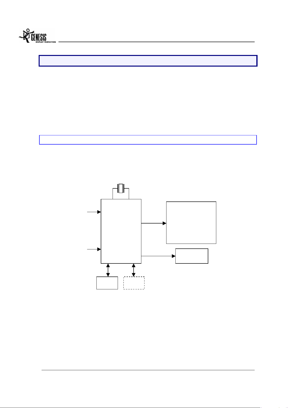
11..11 ggmm55111100//2200 SSyysstteemm DDeessiiggnn EExxaammppllee
Figure 1 below shows a typical dual interface LCD monitor system based on the gm5110/20.
Designs based on the gm5110/20 have reduced system cost, simplified hardware and
firmware design and increased reliability because only a minimal number of components are
required in the system.
NVRAM
EEPROM
(optional)
LCD Module
Back-light
gm5110 /
gm5120
Analog
RGB
DVI
Figure 1. gm5110/20 System Design Example

*** Genesis Microchip Confidential *** gm5110/20 Preliminary Data Sheet
June 2002 C5110-DAT-01C
2
11..22 ggmm55111100//2200 FFeeaattuurreess
FEATURES
• Zoom (from VGA) and shrink (from UXGA) scaling
• Integrated 8-bit triple-channel ADC / PLL
• Integrated Ultra-Reliable DVI 1.0-compliant receiver
• High-Bandwidth Digital Content Protection (HDCP)
• Embedded microcontroller with parallel ROM interface
• On-chip versatile OSD engine
• All system clocks synthesized from a single external crystal
• Programmable gamma correction (CLUT)
• RealColor controls provide sRGB compliance
• PWM back light intensity control
• 5-Volt tolerant inputs
• Low EMI and power saving features
• High-Quality Advanced Scaling
• Fully programmable zoom ratios
• High-quality shrink capability from UXGA resolution
• Real Recovery function provides full color recovery
image for refresh rates higher than those supported by
the LCD panel
• Moire cancellation
• Analog RGB Input Port
• Supports up to 162MHz (SXGA 75Hz / UXGA 60Hz)
• On-chip high-performance PLLs
(only a single reference crystal required)
• Auto-Configuration / Auto-Detection
• Input format detection
• Phase and image positioning
• Ultra-Reliable DVI Compliant Input Port
• Operating up to 165 MHz (up to UXGA 60Hz)
• Direct connect to all DVI compliant digital transmitters
• High-bandwidth Digital Content Protection (HDCP)
• RealColor Technology
• Digital brightness and contrast controls
• TV color controls including hue and saturation controls
• Flesh-tone adjustment
• Full color matrix allows end-users to experience the
same colors as viewed on CRTs and other displays
(e.g. sRGB compliance)
• On-chip OSD Controller
• On-chip RAM for downloadable menus
• 1, 2 and 4-bit per pixel character cells
• Horizontal and vertical stretch of OSD menus
• Blinking, transparency and blending
• On-chip Microcontroller
• Requires no external micro-controller
• External parallel ROM interface allows firmware customization
with little additional cost
• 21 general-purpose inputs/outputs (GPIO's) available for
managing system devices (keypad, back-light, NVRAM, etc)
• Industry-standard firmware embedded on-chip, requires no
external ROM (configuration settings stored in NVRAM)
• Programmable Output Format
• Single / double wide up to XGA 75Hz output for gm5110
and up to SXGA 75Hz output for gm5120
• Pin swap, odd / even swap and red / blue group swap of
RGB outputs for flexibility in board layout
• Support for 8 or 6-bit panels (with high-quality dithering)
• Highly Integrated System-on-a-Chip
Reduces Component Count for Highly Cost
Effective Solution
• Stand-alone operation requires no external
ROM and no firmware development for Fast
Time to Market
• Pin and register compatible Family of Products:
- gm5110/gm5120 Dual-Interface XGA/SXGA
- gm3110/gm3120 Digital-Interface XGA/SXGA
- gm2110/gm2120 Analog-Interface XGA/SXGA

*** Genesis Microchip Confidential *** gm5110/20 Preliminary Data Sheet
June 2002 C5110-DAT-01C
3
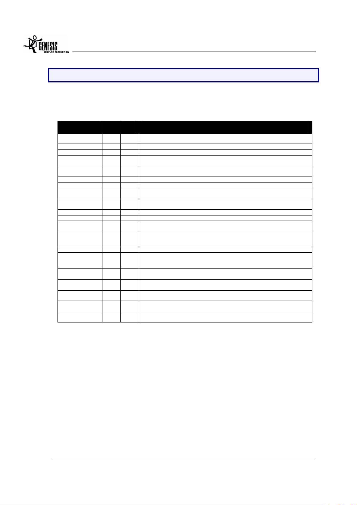
2. GM5110/20 PINOUT
gm5110 and gm5120 are pin-compatible. These devices are available in a 208-pin Plastic
Quad Flat Pack (PQFP) package. Figure 2 provides the pin locations for all signals.
Figure 2. gm5110/20 Pin Out Diagram
RVDD
RVSS
PD0/ER0
PD1/ER1
PD2/ER2
PD3/ER3
PD4/ER4
PD5/ER5
PD6/ER6
PD7/ER7
PD8/EG0
PD9/EG1
PD10/EG2
PD11/EG3
RVDD
RVSS
PD12/EG4
PD13/EG5
PD14/EG6
PD15/EG7
PD16/EB0
PD17/EB1
PD18/EB2
PD19/EB3
PD20/EB4
PD21/EB5
PD22/EB6
PD23/EB7
RVDD
RVSS
PD24/OR0
PD25/OR1
PD26/OR2
PD27/OR3
PD28/OR4
CVDD_2.5
CVSS
PD29/OR5
PD30/OR6
PD31/OR7
PD32/OG0
PD33/OG1
PD34/OG2
PD35/OG3
RVDD
RVSS
PD36/OG4
PD37/OG5
PD38/OG6
PD39/OG7
PD40/OB0
PD41/OB1
GPIO17
RVDD
RVSS
GPIO21/IRQn
RESETn
GPIO14/DDC_SCL
GPIO15/DDC_SDA
ROM_ADDR15
ROM_ADDR14
ROM_ADDR13
ROM_ADDR12
ROM_ADDR11
ROM_ADDR10
ROM_ADDR9
ROM_ADDR8
ROM_ADDR7
ROM_ADDR6
ROM_ADDR5
ROM_ADDR4
RVDD
RVSS
ROM_ADDR3
ROM_ADDR2
ROM_ADDR1
ROM_ADDR0
CVDD_2.5
CVSS
GPI7/ROM_DATA7
GPI6/ROM_DATA6
GPI5/ROM_DATA5
GPI4/ROM_DATA4
GPI3/ROM_DATA3
GPI2/ROM_DATA2
GPI1/ROM_DATA1
GPI0/ROM_DATA0
ROM_Oen
RVDD
RVSS
GPIO8/IRQINn
GPIO0/PWM0
GPIO1/PWM1
GPIO2/PWM2
GPIO3/TIMER1
GPIO4/UART_D1
GPIO5/UART_D0
GPIO6
GPIO7
GPIO9
GPIO10
GPIO11/ROM_WEn
GPIO12/NVRAM_SDA
GPIO13/NVRAM_SCL
5354555657585960616263646566676869707172737475767778798081828384858687888990919293949596979899
100
101
102
103
104
1
2
3
4
5
6
7
8
9
10
11
12
13
14
15
16
17
18
19
20
21
22
23
24
25
26
27
28
29
30
31
32
33
34
35
36
37
38
39
40
41
42
43
44
45
46
47
48
49
50
51
52
156
155
154
153
152
151
150
149
148
147
146
145
144
143
142
141
140
139
138
137
136
135
134
133
132
131
130
129
128
127
126
125
124
123
122
121
120
119
118
117
116
115
114
113
112
111
110
109
108
107
106
105
GND1_ADC
VDD1_ADC_2.5
GND2_ADC
VDD2_ADC_2.5
TCLK
XTAL
AVDD_RPLL
AVSS_RPLL
VDD_RPLL
VSS_RPLL
AVDD_DDDS
AVSS_DDDS
VDD_DDDS
VSS_DDDS
N/C
AVDD_SDDS
AVSS_SDDS
VDD_SDDS
VSS_SDDS
HSYNC
VSYNC
CVSS
CVDD_2.5
CVSS
Reserved
Reserved
RVSS
RVDD
N/C
N/C
GP07
GP06
GP05
GP04
GP03
GP02
GP01
GP00
DCLK
DVS
DHS
DEN
PBIAS
PPWR
RVSS
RVDD
PD47/OB7
PD46/OB6
PD45/OB5
PD44/OB4
PD43/OB3
PD42/OB2
208
207
206
205
204
203
202
201
200
199
198
197
196
195
194
193
192
191
190
189
188
187
186
185
184
183
182
181
180
179
178
177
176
175
174
173
172
171
170
169
168
167
166
165
164
163
162
161
160
159
158
157
GPIO18
GPIO19
GPIO20
GPIO16/HFSn
GPIO22/HCLK
CVDD_2.5
CVSS
CLKOUT
N/C
VDD_RXPLL_2.5
AGND_RXPLL
AGND_RXC
AVDD_RXC
RXC-
RXC+
AVDD_RX0
RX0-
RX0+
AGND_RX0
GND_RX0
VDD_RX0_2.5
AVDD_RX1
RX1-
RX1+
AGND_RX1
GND_RX1
VDD_RX1_2.5
AVDD_RX2
RX2-
RX2+
AGND_RX2
GND_RX2
VDD_RX2_2.5
AGND_IMB
REXT
AVDD_IMB
AVDD_RED
RED+
RED-
AGND_RED
AVDD_GREEN
GREEN+
GREEN-
AGND_GREEN
AVDD_BLUE
BLUE+
BLUE-
AGND_BLUE
AVDD_ADC
ADC_TEST
AGND_ADC
SGND_ADC
gm5110/20
*** Genesis Microchip Confidential *** gm5110/20 Preliminary Data Sheet
June 2002 C5110-DAT-01C
4
3. GM5110/20 PIN LIST
I/O Legend: A = Analog, I = Input, O = Output, P = Power, G= Ground
Table 1. Analog Input Port
Pin Name No. I/O Description
AVDD_RED 172 AP Analog power (3.3V) for the red channel. Must be bypassed with decoupling capacitor to
AGND_RED pin on system board (as close as possible to the pin).
RED+ 171 AI Positive analog input for Red channel.
RED- 170 AI Negative analog input for Red channel.
AGND_RED 169 AG Analog ground for the red channel.
Must be directly connected to the analog system ground plane.
AVDD_GREEN 168 AP Analog power (3.3V) for the green channel. Must be bypassed with decoupling capacitor to
AGND_GREEN pin on system board (as close as possible to the pin).
GREEN+ 167 AI Positive analog input for Green channel.
GREEN- 166 AI Negative analog input for Green channel.
AGND_GREEN 165 AG Analog ground for the green channel.
Must be directly connected to the analog system ground plane.
AVDD_BLUE 164 AP Analog power (3.3V) for the blue channel. Must be bypassed with decoupling capacitor to
AGND_BLUE pin on system board (as close as possible to the pin).
BLUE+ 163 AI Positive analog input for Blue channel.
BLUE- 162 AI Negative analog input for Blue channel.
AGND_BLUE 161 AG Analog ground for the blue channel.
Must be directly connected to the analog system ground plane.
AVDD_ADC 160 AP Analog power (3.3V) for ADC analog blocks that are shared by all three channels. Includes
band gap reference, master biasing and full-scale adjust. Must be bypassed with
decoupling capacitor to AGND_ADC pin on system board (as close as possible to the pin).
ADC_TEST 159 AO Analog test output for ADC Do not connect.
AGND_ADC 158 AG Analog ground for ADC analog blocks that are shared by all three channels. Includes band
gap reference, master biasing and full-scale adjust.
Must be directly connected to analog system ground plane.
SGND_ADC 157 AG Dedicated pad for substrate guard ring that protects the ADC reference system.
Must be directly connected to the analog system ground plane.
GND1_ADC 156 G Digital GND for ADC clocking circuit.
Must be directly connected to the digital system ground plane
VDD1_ADC_2.5 155 P Digital power (2.5V) for ADC encoding logic. Must be bypassed with decoupling capacitor to
GND1_ADC pin on system board (as close as possible to the pin).
GND2_ADC 154 G Digital GND for ADC clocking circuit.
Must be directly connected to the digital system ground plane.
VDD2_ADC_2.5 153 P Digital power (2.5V) for ADC encoding logic. Must be bypassed with decoupling capacitor to
GND2_ADC pin on system board (as close as possible to the pin).
*** Genesis Microchip Confidential *** gm5110/20 Preliminary Data Sheet
June 2002 C5110-DAT-01C
5
Table 2. DVI Input Port
Pin Name No I/O Description
AVDD_IMB 173 AP Analog VDD (3.3V) for internal biasing circuits.
Must be bypassed with decoupling capacitors (as close as possible to the pin).
REXT 174 AI External reference resistor.
An external 1Kohm (1%) resistor should be connected from this pin to AVDD_IMB pin.
AGND_IMB 175 AG Analog GND for internal biasing circuits.
Must be connected directly to the ground plane.
VDD_RX2_2.5 176 P VDD (2.5V) for DVI input pair 2 logic circuits. Must be bypassed with decoupling capacitor to
GND_RX2 pin (as close as possible to the pin).
GND_RX2 177 G GND for DVI input pair 2 logic circuits.
Must be connected directly to the ground plane.
AGND_RX2 178 AG Analog GND for DVI input pair 2 input buffer.
Must be connected directly to the analog ground plane.
RX2+ 179 AI DVI input pair 2
RX2- 180 AI DVI input pair 2
AVDD_RX2 181 AP Analog VDD (3.3V) for DVI input pair 2 input buffer. Must be bypassed with decoupling
capacitor to AGND_RX2 pin (as close as possible to the pin).
VDD_RX1_2.5 182 P VDD (2.5V) for DVI input pair 1 logic circuits. Must be bypassed with decoupling capacitor to
GND_RX1 pin (as close as possible to the pin).
GND_RX1 183 G GND for DVI input pair 1 input buffer.
Must be connected directly to the analog ground plane.
AGND_RX1 184 AG Analog GND for DVI input pair 1 input buffer.
Must be connected directly to the analog ground plane.
RX1+ 185 AI DVI input pair 1
RX1- 186 AI DVI input pair 1
AVDD_RX1 187 AP Analog VDD (3.3V) for DVI input pair 1 input buffer. Must be bypassed with decoupling
capacitor to AGND_RX1 pin (as close as possible to the pin).
VDD_RX0_2.5 188 P VDD (2.5V) for DVI input pair 0 logic circuits. Must be bypassed with decoupling capacitor to
GND_RX0 pin (as close as possible to the pin).
GND_RX0 189 G GND for DVI input pair 0 logic circuits.
Must be connected directly to the ground plane.
AGND_RX0 190 AG Analog GND for DVI input pair 0 input buffer.
Must be connected directly to the analog ground plane.
RX0+ 191 AI DVI input pair 0
RX0- 192 AI DVI input pair 0
AVDD_RX0 193 AP Analog VDD (3.3V) for DVI input pair 0 input buffer. Must be bypassed with decoupling
capacitor to AGND_RX0 pin (as close as possible to the pin).
RXC+ 194 AI DVI input clock pair
RXC- 195 AI DVI input clock pair
AVDD_RXC 196 AP Analog VDD (3.3V) for DVI input clock pair input buffer. Must be bypassed with 100pF
capacitor to AGND_RXC pin (as close as possible to the pin).
AGND_RXC 197 AG Analog GND for DVI input clock pair input buffer.
Must be connected directly to the analog ground plane.
GND_RXPLL 198 G Digital GND for the DVI receiver internal PLL.
Must be connected directly to the system ground plane.
VDD_RXPLL_2.5 199 AP Analog VDD (2.5V) for the DVI receiver internal PLL. Must be bypassed with a decoupling
capacitor to AGND_RXPLL pin (as close as possible to the pin).
CLKOUT 201 AO For test purposes only. Do not connect.
Table 3. RCLK PLL Pins
Pin Name No I/O Description
AVDD_RPLL 150 AP Analog power for the Reference DDS PLL. Connect to 3.3V supply. Must be bypassed with a
0.1uF capacitor to pin AVSS_RPLL (as close to the pin as possible).
AVSS_RPLL 149 AG Analog ground for the Reference DDS PLL.
Must be directly connected to the analog system ground plane.
TCLK 152 AI Reference clock (TCLK) from the 14.3MHz crystal oscillator, or from single-ended
CMOS/TTL clock oscillator (refer to Figure 7). This is a 5V-tolerant input.
XTAL 151 AO Crystal oscillator output.
VDD_RPLL 148 P Digital power for RCLK PLL. Connect to 3.3V supply.
VSS_RPLL 147 G Digital ground for RCLK PLL.
*** Genesis Microchip Confidential *** gm5110/20 Preliminary Data Sheet
June 2002 C5110-DAT-01C
6
Table 4. Analog HSYNC/VSYNC Inputs
Pin Name No I/O Description
HSYNC 137 I ADC input horizontal sync input.
[Input, Schmitt trigger (400mV typical hysteresis), 5V-tolerant]
VSYNC 136 I ADC input vertical sync input.
[Input, Schmitt trigger (400mV typical hysteresis), 5V-tolerant]
Table 5. System Interface and GPIO Signals
Pin Name No I/O Description
RESETn 5 I
Active-low hardware reset signal. The reset signal must be held low for at least 1µS.
[Input, Schmitt trigger (400mV typical hysteresis), 5V-tolerant]
GPIO0/PWM0 40 IO General-purpose input/output signal or PWM0. Open drain option via register setting.
[Bi-directional, Schmitt trigger (400mV typical hysteresis), 5V-tolerant]
GPIO1/PWM1 41 IO General-purpose input/output signal or PWM1. Open drain option via register setting.
[Bi-directional, Schmitt trigger (400mV typical hysteresis), 5V-tolerant]
GPIO2/PWM2 42 IO General-purpose input/output signal or PWM2. Open drain option via register setting.
[Bi-directional, Schmitt trigger (400mV typical hysteresis), 5V-tolerant]
GPIO3/TIMER1 43 IO General-purpose input/output signal. Open drain option via register setting. This pin is also
connected to Timer 1 clock input of the OCM.
[Bi-directional, Schmitt trigger (400mV typical hysteresis), 5V-tolerant]
GPIO4/UART_DI 44 IO General-purpose input/output signal. Open drain option via register setting. This pin is also
connected to the OCM UART data input signal by programming an OCM register.
[Bi-directional, Schmitt trigger (400mV typical hysteresis), 5V-tolerant]
GPIO5/UART_DO 45 IO General-purpose input/output signal. Open drain option via register setting. This pin is also
connected to the OCM UART data output signal by programming an OCM register.
[Bi-directional, Schmitt trigger (400mV typical hysteresis), 5V-tolerant]
GPIO6 46 IO General-purpose input/output signal.
[Bi-directional, Schmitt trigger (400mV typical hysteresis), 5V-tolerant]
GPIO7 47 IO General-purpose input/output signal.
[Bi-directional, Schmitt trigger (400mV typical hysteresis), 5V-tolerant]
GPIO8/IRQINn 39 IO General-purpose input/output signal. This is also active-low interrupt input to OCM and is
directly wired to OCM int_0n.
[Bi-directional, Schmitt trigger (400mV typical hysteresis), 5V-tolerant]
GPIO9 48 IO General-purpose input/output signal. Open drain option via register setting.
[Bi-directional, Schmitt trigger (400mV typical hysteresis), 5V-tolerant]
GPIO10 49 IO General-purpose input/output signal. Open drain option via register setting.
[Bi-directional, Schmitt trigger (400mV typical hysteresis), 5V-tolerant]
GPIO11/ROM_WEn
50 IO General-purpose input/output or PROM write enable signal. Open drain option via register
setting. [Bi-directional Input, Schmitt trigger (400mV typical hysteresis), 5V-tolerant]
GPIO12/NVRAM_SDA
GPIO13/NVRAM_SCL
51
52
IO
IO
General-purpose input/output or master 2-wire serial interface to NVRAM in standalone
operation. Open drain option via register setting. [Bi-directional Input, Schmitt trigger
(400mV typical hysteresis), 5V-tolerant]
GPIO14/DDC_SCL 6 I DDC Interface for DVI-HDCP communication. This is 5V-tolerant SCL pin.
GPIO15/DDC_SDA 7 IO DDC Interface for DVI-HDCP communication. This is 5V-tolerant SDA pin.
GPIO16/HFSn 205 IO General-purpose input/output signal when host interface is disabled, or host interface
framing signal.
[Bi-directional, Schmitt trigger (400mV typical hysteresis), slew rate limited, 5V tolerant]
GPIO17
GPIO18
GPIO19
GPIO20
1
208
207
206
IO
IO
IO
IO
General-purpose input/output signal.
[Bi-directional, Schmitt trigger (400mV typical hysteresis), 5V-tolerant]
GPIO21/IRQn 4 IO General-purpose input/output signal when host port is disabled, or active-low and open-
drain interrupt output pin.
[Bi-directional, 5V-tolerant]
GPIO22/HCLK 204 IO General-purpose input/output signal when host interface is disabled, or host clock signal.
[Bi-directional, Schmitt trigger (400mV typical hysteresis), 5V-tolerant]
GPO0
GPO1
GPO2
GPO3
GPO4
GPO5
GPO6
GPO7
119
120
121
122
123
124
125
126
O
O
O
O
O
O
O
O
General-purpose output signals.
*** Genesis Microchip Confidential *** gm5110/20 Preliminary Data Sheet
June 2002 C5110-DAT-01C
7
Table 6. Display Output Port
Pin Name No I/O Description
DCLK 118 O Panel output clock.
[Tri-state output, Programmable Drive]
DVS 117 O Panel Vertical Sync.
[Tri-state output, Programmable Drive]
DHS 116 O Panel Horizontal Sync.
[Tri-state output, Programmable Drive]
DEN 115 O Panel Display Enable, which frames the output background.
[Tri-state output, Programmable Drive]
PBIAS 114 O Panel Bias Control (back light enable)
[Tri-state output, Programmable Drive]
PPWR 113 O Panel Power Control
[Tri-state output, Programmable Drive]
PD47
PD46
PD45
PD44
PD43
PD42
PD41
PD40
PD39
PD38
PD37
PD36
PD35
PD34
PD33
PD32
PD31
PD30
PD29
PD28
PD27
PD26
PD25
PD24
PD23
PD22
PD21
PD20
PD19
PD18
PD17
PD16
PD15
PD14
PD13
PD12
PD11
PD10
PD9
PD8
PD7
PD6
PD5
PD4
PD3
PD2
PD1
PD0
110
109
108
107
106
105
104
103
102
101
100
99
96
95
94
93
92
91
90
87
86
85
84
83
80
79
78
77
76
75
74
73
72
71
70
69
66
65
64
63
62
61
60
59
58
57
56
55
O
O
O
O
O
O
O
O
O
O
O
O
O
O
O
O
O
O
O
O
O
O
O
O
O
O
O
O
O
O
O
O
O
O
O
O
O
O
O
O
O
O
O
O
O
O
O
O
Panel output data.
[Tri-state output, Programmable Drive]

*** Genesis Microchip Confidential *** gm5110/20 Preliminary Data Sheet
June 2002 C5110-DAT-01C
8
Table 7. Parallel ROM Interface Port
Pin Name No I/O Description
ROM_ADDR15
ROM_ADDR14
ROM_ADDR13
ROM_ADDR12
ROM_ADDR11
ROM_ADDR10
ROM_ADDR9
ROM_ADDR8
ROM_ADDR7
ROM_ADDR6
ROM_ADDR5
ROM_ADDR4
ROM_ADDR3
ROM_ADDR2
ROM_ADDR1
ROM_ADDR0
8
9
10
11
12
13
14
15
16
17
18
19
22
23
24
25
IO
IO
IO
IO
IO
IO
IO
IO
IO
IO
IO
IO
IO
IO
IO
IO
ROM address output. These pins also serve as 5V-tolerant bootstrap inputs on power up.
GPI7/ROM_DATA7
GPI6/ROM_DATA6
GPI5/ROM_DATA5
GPI4/ROM_DATA4
GPI3/ROM_DATA3
GPI2/ROM_DATA2
GPI1/ROM_DATA1
GPI0/ROM_DATA0
28
29
30
31
32
33
34
35
I
I
I
I
I
I
I
I
5V-tolerant external PROM data input, or general-purpose input in standalone operation.
ROM_OEn 36 O External PROM data Output Enable
Table 8. Reserved Pins
Pin Name No I/O Description
N/C 127 O No connect.
N/C 128 O No connect.
Reserved 131 I Tie to GND.
Reserved 132 I Tie to GND.
N/C 142 O No connect.
N/C 200 O No connect.

*** Genesis Microchip Confidential *** gm5110/20 Preliminary Data Sheet
June 2002 C5110-DAT-01C
9
Note that VDD pins having "_2.5" in their names should be connected to 2.5V power supplies. All
other VDD pins should be connected to 3.3V power supplies.
Table 9. Power Pins for ADC Sampling Clock DDS
Pin Name No I/O Description
AVDD_DDDS 146 AP Analog power for the Destination DDS. Connect to 3.3V supply.
Must be bypassed with a 0.1uF capacitor to AVSS_DDDS pin
(as close to the pin as possible).
AVSS_DDDS 145 AG Analog ground for the Destination DDS.
Must be directly connected to the analog system ground.
VDD_DDDS 144 P Digital power for the Destination DDS. Connect to 3.3V supply.
VSS_DDDS 143 G Digital ground for the Destination DDS.
Table 10. Power Pins for Display Clock DDS
Pin Name No I/O Description
AVDD_SDDS 141 AP Analog power for Source DDS. Connect to 3.3V supply.
Must be bypassed with a 0.1uF capacitor to AVSS_SDDS pin
(as close to the pin as possible).
AVSS_SDDS 140 AG Analog ground for Source DDS.
Must be directly connected to the analog system ground plane.
VDD_SDDS 139 P Digital power for the Source DDS. Connect to 3.3V supply.
VSS_SDDS 138 G Digital ground for the Source DDS.
Table 11. I/O Power and Ground Pins
Pin Name No I/O Description
RVDD 2
20
37
53
67
81
97
111
129
P
P
P
P
P
P
P
P
P
Connect to 3.3V supply.
Must be bypassed with a 0.1uF capacitor to RVSS (as close to the pin as possible).
RVSS 3
21
38
54
68
82
98
112
130
G
G
G
G
G
G
G
G
G
Connect to digital ground.
Table 12. Core Power and Ground Pins
Pin Name No I/O Description
CVDD_2.5 26
88
134
203
P
P
P
P
Connect to 2.5V supply.
Must be bypassed with a 0.1uF capacitor to CVSS (as close to the pin as possible).
CVSS 27
89
133
135
202
G
G
G
G
G
Connect to digital ground.
 Loading...