

SMBG AND SMBJ5.0 THRU 170CA
SURFACE MOUNT TRANSZORB™ TRANSIENT VOLTAGE SUPPRESSOR
Stand-off Voltage - 5.0 to170 Volts Peak Pulse Power - 600 Watts
FEATURES
♦ Plastic package has Underwriters Laboratory Flammability
Classification 94V-0
♦ For surface mounted applications in order to optimize
board space
♦ Low profile package
♦ Built-in strain relief
♦ Glass passivated junction
♦ Low incremental surge resistance
♦ 600W peak pulse power capability with a 10/1000µs
waveform, repetition rate (duty cycle): 0.01%
♦ Excellent clamping capability
♦ Fast response time: typically less than 1.0ps from 0 volts
to V
(BR)
for unidirectional and 5.0ns for bidirectional types
♦ For devices with V
(BR)
≥10V, IDare typically less
than 1.0µA
♦ High temperature soldering guaranteed:
250°C/10 seconds at terminals
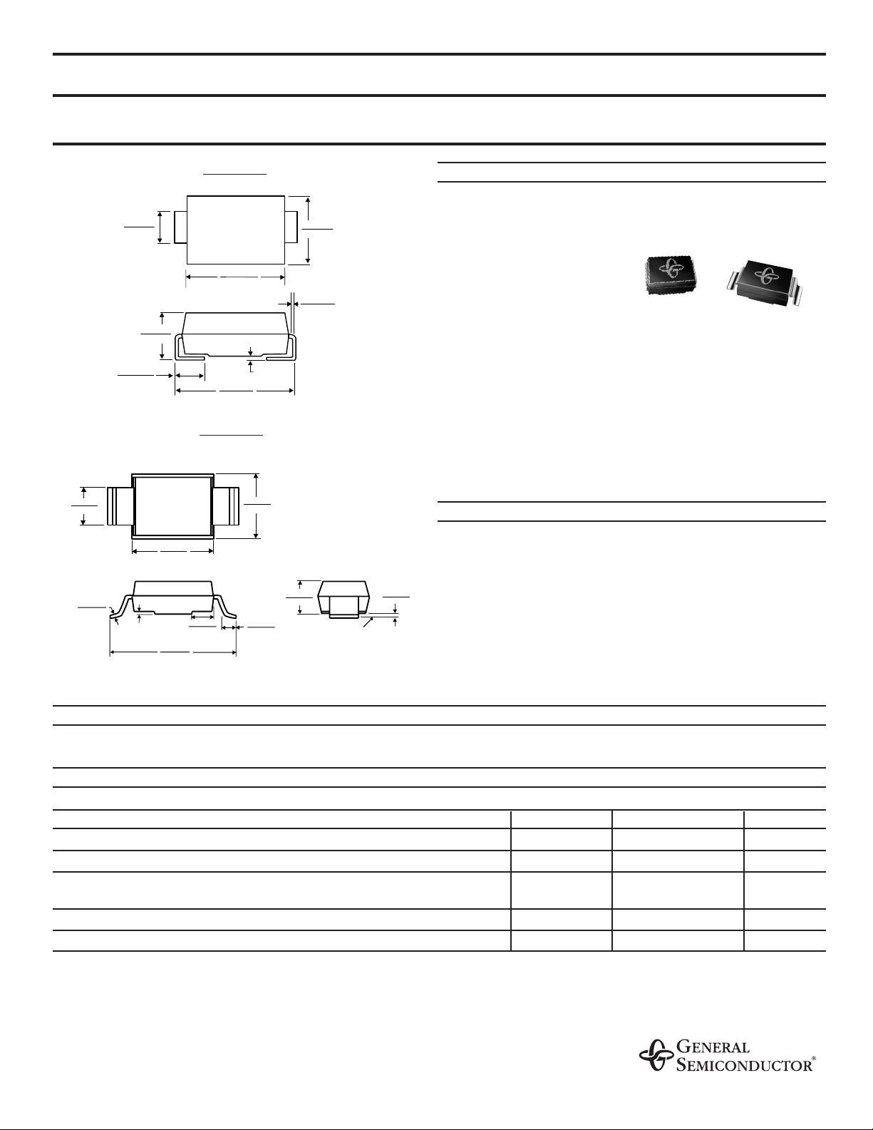
MECHANICAL DATA
Case: JEDEC DO214AA / DO215AA molded plastic body
over passivated junction
Terminals: Solder plated, solderable per MIL-STD-750,
Method 2026
Polarity: For unidirectional types the color band denotes the
cathode, which is postitive with respect to the anode under
normal TVS operation
Mounting Position: Any
Weight: 0.003 ounces, 0.093 gram
DEVICES FOR BIDIRECTIONAL APPLICATIONS
For bidirectional use suffix C or CA for types SMB-5.0 thru SMB-170 (eg. SMBG5.0C, SMBJ170CA).
Electrical characteristics apply in both directions
MAXIMUM RATINGS AND ELECTRICAL CHARACTERISTICS
Ratings at 25°C ambient temperature unless otherwise specified.
SYMBOLS VALUE UNITS
Peak pulse power dissipation with a 10/1000µs waveform
(NOTES 1, 2, FIG. 1)
P
PPM
Minimum 600 Watts
Peak pulse current with a 10/1000µs waveform
(NOTE 1)
I
PPM SEE TABLE 1
Amps
Peak forward surge current 8.3ms single half sine-wave superimposed
on rated load (JEDEC Method)
(NOTES 2, 3)
- unidirectional only
I
FSM
100.0 Amps
Maximum instantaneous forward voltage at 50A
(NOTE 3)
unidirectional only V
F
3.5 Volts
Operating junction and storage temperature range TJ, T
STG
-55 to +150 °C
NOTES:
(1) Non-repetitive current pulse, per Fig.3 and derated above TA=25°C per Fig. 2
(2) Mounted on 0.2 x 0.2” (5.0 x 5.0mm) copper pads to each terminal
(3) Measured on 8.3ms single half sine-wave. For uni-directional devices only.
DO-215AA
GULL WING
DO-214AA
MODIFIED J-BEND
Dimensions in inches and (millimeters)
2/1/99
0.125 (3.17)
0.115 (2.92)
0.016 (0.41)
0.006 (0.15)
0.086 (2.20)
0.077 (1.95)
0.180 (4.57)
0.160 (4.06)
0.096 (2.44)
0.084 (2.13)
0.220 (5.59)
0.205 (5.21)
0.008 (0.203)
0.060 (1.52)
0.030 (0.76)
0.245 (6.22)
0.130 (5.72)
0.280 (7.11)
0.260 (6.60)
0.400 (10.16)
0.380 (9.64)
0.058 (1.47)
0.038 (0.97)
0.020
(0.51)
MAX.
0.032 (8.10)
0.024 (6.10)
MAX.
0.155 (3.94)
0.130 (3.30)
0.012 (0.305)
0.006 (0.152)
0.095 (2.41)
0.075 (1.90)
SEATING
PLANE
0.008 (0.20)
0.004 (0.10)

ELECTRICAL CHARACTERISTICS (T
A
=25°C unless otherwise noted) TABLE 1
Breakdown Maximum Maximum
Device Voltage Reverse Peak Pulse Maximum
Device Type Device Type Marking V
(BR)
(Volts) Test Stand-off Leakage I
D
Surge Clamping
Gull Wing Modified Code
(NOTE 1)
Current Voltage at V
WM
Current I
PPM
Voltage at I
PPM
Lead “J” Bend Lead UNI BI (MIN /MAX) at IT(mA) VWM(Volts) (µA)
(NOTE 3) (NOTE 2)
(Amps) VC(Volts)
SMBG5.0 SMBJ5.0 KD 6.40 / 7.82 10 5.0 800 62.5 9.6
SMBG5.0A SMBJ5.0A KE 6.40 / 7.07 10 5.0 800 65.2 9.2
SMBG6.0 SMBJ6.0 KF 6.67 / 8.15 10 6.0 800 52.6 11.4
SMBG6.0A SMBJ6.0A KG 6.67 / 7.37 10 6.0 800 58.3 10.3
SMBG6.5 SMBJ6.5 KH 7.22 / 8.82 10 6.5 500 48.8 12.3
SMBG6.5A SMBJ6.5A KK 7.22 / 7.98 10 6.5 500 53.6 11.2
SMBG7.0 SMBJ7.0 KL 7.78 / 9.51 10 7.0 200 45.1 13.3
SMBG7.0A SMBJ7.0A KM 7.78 / 8.60 10 7.0 200 50.0 12.0
SMBG7.5 SMBJ7.5 KN 8.33 / 10.2 1.0 7.5 100 42.0 14.3
SMBG7.5A SMBJ7.5A KP 8.33 / 9.21 1.0 7.5 100 46.5 12.9
SMBG8.0 SMBJ8.0 KQ 8.89 / 10.9 1.0 8.0 50 40.0 15.0
SMBG8.0A SMBJ8.0A KR 8.89 / 9.83 1.0 8.0 50 44.1 13.6
SMBG8.5 SMBJ8.5 KS 9.44 / 11.5 1.0 8.5 20 37.7 15.9
SMBG8.5A SMBJ8.5A KT 9.44 / 10.4 1.0 8.5 20 41.7 14.4
SMBG9.0 SMBJ9.0 KU 10.0 / 12.2 1.0 9.0 10 35.5 16.9
SMBG9.0A SMBJ9.0A KV 10.0 / 11.1 1.0 9.0 10 39.0 15.4
SMBG10 SMBJ10 KW 11.1 / 13.6 1.0 10 5.0 31.9 18.8
SMBG10A SMBJ10A KX 11.1 / 12.3 1.0 10 5.0 35.3 17.0
SMBG11 SMBJ11 KY 12.2 / 14.9 1.0 11 5.0 29.9 20.1
SMBG11A SMBJ11A KZ 12.2 / 13.5 1'0 11 5.0 33.0 18.2
SMBG12 SMBJ12 LD 13.3 / 16.3 1.0 12 5.0 27.3 22.0
SMBG12A SMBJ12A LE 13.3 / 14.7 1.0 12 5.0 30.2 19.9
SMBG13 SMBJ13 LF 14.4 / 17,6 1.0 13 5.0 25.2 23.8
SMBG13A SMBJ13A LG 14.4 / 15.9 1.0 13 5.0 27.9 21.5
SMBG14 SMBJ14 LH 15,6 / 19.1 1.0 14 5.0 23.3 25.8
SMBG14A SMBJ14A LK 15.6 / 17.2 1.0 14 5.0 25.9 23.2
SMBG15 SMBJ15 LL 16.7 / 20.4 1.0 15 5.0 22.3 26.9
SMBG15A SMBJ15A LM 16.7 / 18.5 1.0 15 5.0 24.6 24.4
SMBG16 SMBJ16 LN 178 / 21.8 1.0 16 5.0 20.8 28.8
SMBG16A SMBJ16A LP 178 / 19.7 1.0 16 5.0 23.1 26.0
SMBG17 SMBJ17 LQ 18.9 / 23.1 1.0 17 5.0 19.7 30.5
SMBG17A SMBJ17A LR 18.9 / 20.9 1.0 17 5.0 21.7 27.6
SMBG18 SMBJ18 LS 20.0 / 24.4 1.0 18 5.0 18.6 32.2
SMBG18A SMBJ18A LT 20.0 / 22.1 1.0 18 5.0 20.5 29.2
SMBG20 SMBJ20 LU 22.2 / 27.1 1.0 20 5.0 16.8 35.8
SMBG20A SMBJ20A LV 22.2 / 24.5 1.0 20 5.0 18.5 32.4
SMBG22 SMBJ22 LW 24.4 / 29.8 1.0 22 5.0 15.2 39.4
SMBG22A SMBJ22A LX 24.4 / 26.9 1.0 22 5.0 16.9 35.5
SMBG24 SMBJ24 LY 26.7 / 32.6 1.0 24 5.0 14.0 43.0
SMBG24A SMBJ24A LZ 26.7 / 29.5 1.0 24 5.0 15.4 38.9
SMBG26 SMBJ26 MD 28.9 / 35.3 1.0 26 5.0 12.9 46.6
SMBG26A SMBJ26A ME 28.9 / 31.9 1.0 26 5.0 14.3 42.1
SMBG28 SMBJ28 MF 31.1 / 38.0 1.0 28 5.0 12.0 50.0
SMBG28A SMBJ28A MG 31.1 / 34.4 1.0 28 5.0 13.2 45.4
SMBG30 SMBJ30 MH 33.3 / 40.7 1.0 30 5.0 11.2 53.5
SMBG30A SMBJ30A MK 33.3 / 36.8 1.0 30 5.0 12.4 48.4
SMBG33 SMBJ33 ML 36.7 / 44.9 1.0 33 5.0 10.2 59.0
SMBG33A SMBJ33A MM 36.7 / 40.6 1.0 33 5.0 11.3 53.3
SMBG36 SMBJ36 MN 40.0 / 48.9 1.0 36 5.0 9.3 64.3
SMBG36A SMBJ36A MP 40.0 / 44.2 1.0 36 5.0 10.3 58.1
SMBG40 SMBJ40 MQ 44.4 / 54.3 1.0 40 5.0 8.4 71.4
SMBG40A SMBJ40A MR 44.4 / 49.1 1.0 40 5.0 9.3 64.5
SMBG43 SMBJ43 MS 47.8 / 58.4 1.0 43 5.0 7.8 76.7
SMBG43A SMBJ43A MT 47.8 / 52.8 1.0 43 5.0 8.6 69.4
SMBG45 SMBJ45 MU 50.0 / 61.1 1.0 45 5.0 7.5 80.3
SMBG45A SMBJ45A MV 50.0 / 55.3 1.0 45 5.0 8.3 72.7
SMBG48 SMBJ48 MW 53.3 / 65.1 1.0 48 5.0 7.0 85.5
SMBG48A SMBJ48A MX 53.3 / 58.9 1.0 48 5.0 7.8 77.4
SMBG51 SMBJ51 MY 56.7 / 69-3 1.0 51 5.0 6.6 91.1
SMBG51A SMBJ51A MZ 56.7 / 62.7 1.0 51 5.0 7.3 82.4
KD
KE
KF
KG
AH
AK
KL
KM
AN
AP
AQ
AR
AS
AT
AU
AV
AW
AX
KY
KZ
BD
BE
LF
LG
BH
BK
BL
BM
LN
LM
LQ
LR
BS
BT
LU
LV
BW
BX
BY
BZ
CD
CE
MF
MG
CH
CK
CL
CM
CN
CP
CQ
CR
CS
CT
MU
MV
MW
MX
MY
MZ

ELECTRICAL CHARACTERISTICS (T
A
= 25°C unless otherwise noted) TABLE 1 (Cont’d)
Breakdown Maximum Maximum
Device Voltage Reverse Peak Pulse Maximum
Device Type Device Type Marking V
(BR)
(Volts) Test Stand-off Leakage I
D
Surge Clamping
Gull Wing Modified Code
(NOTE 1)
Current Voltage at V
WM
Current I
PPM
Voltage at I
PPM
Lead “J” Bend Lead UNI BI (Min /Max) at IT(mA) VWM(Volts) (µA)
(NOTE 3) (NOTE 2)
(Amps) VC(Volts)
SMBG54 SMBJ54 ND 60.0 / 73.3 1.0 54 5.0 6.2 96.3
SMBG54A SMBJ54A NE 60.0 / 66.3 1.0 54 5.0 6.9 87.1
SMBG58 SMBJ58 NF 64.4 / 78.7 1.0 58 5.0 5.8 103
SMBG58A SMBJ58A NG 64.4 / 71.2 1.0 58 5.0 6.4 93.6
SMBG60 SMBJ60 NH 66.7 / 81.5 1.0 60 5.0 5.6 107
SMBG60A SMBJ60A NK 66.7 / 73.7 1.0 60 5.0 6.2 96.8
SMBG64 SMBJ64 NL 71.1 / 86.9 1.0 64 5.0 5.3 114
SMBG64A SMBJ64A NM 71.1 / 78.6 1.0 64 5.0 5.8 103
SMBG70 SMBJ70 NN 77.8 / 95.1 1.0 70 5.0 4.8 125
SMBG70A SMBJ70A NP 77.8 / 86.0 1.0 70 5.0 5.3 113
SMBG75 SMBJ75 NQ 83.3 / 102 1.0 75 5.0 4.5 134
SMBG75A SMBJ75A NR 83.3 / 92.1 1.0 75 5.0 5.0 121
SMBG78 SMBJ78 NS 86.7 / 106 1.0 78 5.0 4.3 139
SMBG78A SMBJ78A NT 86.7 / 95.8 1.0 78 5.0 4.8 126
SMBG85 SMBJ85 NU 94.4 / 115 1.0 85 5.0 4.0 151
SMBG85A SMBJ85A NV 94.4 / 104 1.0 85 5.0 4.4 137
SMBG90 SMBJ90 NW 100 / 122 1.0 90 5.0 3.8 160
SMBG90A SMBJ90A NX 100 / 111 1.0 90 6.0 4.1 146
SMBG100 SMBJ100 NY 111 / 136 1.0 100 5.0 3.4 179
SMBG100A SMBJ100A NZ 111 / 123 1.0 100 5.0 3.7 162
SMBG110 SMBJ110 PD 122 / 149 1.0 110 5.0 3.1 196
SMBG110A SMBJ110A PE 122 / 135 1.0 110 5.0 3.4 177
SMBG120 SMBJ120 PF 133 / 163 1.0 120 5.0 2.8 214
SMBG120A SMBJ120A PG 133 / 147 1.0 120 5.0 3.1 193
SMBG130 SMBJ130 PH 144 / 176 1.0 130 5.0 2.6 231
SMBG130A SMBJ130A PK 144 / 159 1.0 130 5.0 2.9 209
SMBG150 SMBJ150 PL 167 / 204 1.0 150 5.0 2.2 268
SMBG150A SMBJ150A PM 167 / 185 1.0 150 5.0 2.5 243
SMBG160 SMBJ160 PN 178 / 218 1.0 160 5.0 2.1 287
SMBG160A SMBJ160A PP 178 / 197 1.0 160 5.0 2.3 259
SMBG170 SMBJ170 PQ 189 / 231 1.0 170 5.0 2.0 304
SMBG170A SMBJ170A PR 189 / 209 1.0 170 5.0 2.2 275
NOTES:
(1) V
(BR)
measured after ITapplied for 300µs square wave pulse or equivalent
(2) Surge current waveform per Fig. 3 and derate per Fig. 2
(3) For bi-directional types having V
WM
of 10 Volts and less, the ID limit is doubled
(4) For the bi-directional SMBG/SMBJ5.0CA, the maximum V
(BR)
is 7.25 Volts
(5) All terms and symbols are consistent with ANSI/IEEE C62.35
APPLICATION N0TES
These surface mountable packages are designed specifically for transient voltage suppression. The wide leads assure a large surface contact for good heat dissipation, and a low resistance path for surge current flow to ground. These high speed transient voltage
suppressors can be used to effectively protect sensitive components such as integrated circuits and MOS devices.
A 600W (SMB) device is normally selected when the threat of transients is from lightening-induced transients conducted via external
leads or 1/0 lines. It is also used to protect against switching transients induced by large coils or industrial motors.
System impedance at component level in a system is usually high enough to limit the current to within the peak pulse current (I
PP
)
rating of this series.
RECOMMENDED PAD SIZES
The pad dimensions should be 0.010” (0.25mm) longer than the contact size, in the lead axis.
This allows a solder fillet to form, see Fig. below. Contact factory for soldering methods.
0.165" (4.19)
0.085" (2.16)
0.050" (1.27)
0.090" (2.28)
0.085" (2.16)
0.070" (1.78)
GULL- WING
MODIFIED J-BEND
ND
NE
NF
NG
NH
NK
NL
NM
NN
NP
NQ
NR
NS
NT
NU
NV
NW
NX
NY
NZ
PD
PE
PF
PG
PH
PK
PL
PM
PN
PP
PQ
PR

MAXIMUM RATINGS AND CHARACTERISTIC CURVES SMBG AND SMBJ5.0 THRU 170CA
FIG. 1 - PEAK PULSE POWER RATING CURVE
P
PPM
, PEAK PULSE POWER, kW
td, PULSE WIDTH, sec.
TA, AMBIENT TEMPERATURE, °C
FIG. 4 - TYPICAL JUNCTION CAPACITANCE
UNIDIRECTIONAL
FIG. 3 - PULSE WAVEFORM
t, TIME, ms
VWM, REVERSE STAND-OFF VOLTAGE, VOLTS
V
WM,
REVERSE STAND-OFF VOLTAGE,
VOLTS
NUMBER OF CYCLES AT 60 H
Z
I
PPM,
PEAK PULSE CURRENT, %
PEAK PULSE POWER (P
PP
) or CURRENT (I
PP
)
DERATING IN PERCENTAGE, %
C
J
, JUNCTION CAPACITANCE, pF
C
J
, JUNCTION CAPACITANCE, pF
I
FSM,
PEAK FORWARD SURGE CURRENT,
AMPERES
NON-REPETITIVE
PULSE WAVEFORM
SHOWN IN FIG. 3
TA=25°C
PULSE WIDTH (td) is DEFINED
as the POINTWHERE the PEAK
CURRENT DECAYS to 50% of I
PPM
tr=10µsec.
MEASURED at
ZERO BIAS
MEASURED at
STAND-OFF
VOLTAGE, V
WM
8.3ms SINGLE HALF SINE-WAVE
(JEDEC Method)
UNIDIRECTIONAL ONLY
td
HALF VALUE - I
PP
2
10/1000µsec. WAVEFORM
as DEFINED byR.E.A.
FIG. 6 - MAXIMUM NON-REPETITIVE PEAK FORWARD
SURGE CURRENT
PEAK VALUE
I
PPM
FIG. 5 - TYPICAL JUNCTION CAPACITANCE
BIDIRECTIONAL
FIG. 2 - PULSE DERATING CURVE
TJ=25° C
f=1.0 MH
Z
Vsig=50mVp-p
TJ=25° C
f=1.0 MH
Z
Vsig=50mVp-p
0.2 x 0.2” (0.5 x 0.5mm)
COPPER PADAREAS
MEASURED at
ZERO BIAS
MEASURED at
STAND-OFF
VOLTAGE, V
WM
100
10
1.0
0.1
µ
s
0.1
1.0
µ
s
150
100
50
0
0
1.0
10
µ
s
100
µ
s
2.0
1.0ms
3.0
10ms
4.0
100
75
50
25
0
0 25 50 75 100 125 150 175 200
6,000
1,000
100
6,000
1,000
100
10
1
10
100 200
10
1
10
200
100
10
1
10
100 200
100
 Loading...