RMB2S THRU RMB4S
MINIATURE GLASS PASSIVATED SINGLE-PHASE SURFACE MOUNT
FAST RECOVERY BRIDGE RECTIFIER
Reverse Voltage - 200 to 400 Volts Forward Current - 0.5 Ampere
FEATURES
♦ Plastic package has Underwriters Laboratory Flammability
Classification 94V-0
♦ This series is UL recognized under Component Index,
file number E54214
♦ Glass passivated chip junctions
♦ High surge overload rating: 35A peak
♦ Saves space on printed circuit boards
♦ Fast recovery, low loss switching
♦ High temperature soldering guaranteed:
260°C/10 seconds at 5 lbs. (2.3kg) tension
MECHANICAL DATA
Case: Molded plastic body over passivated junctions
Terminals: Plated leads solderable per MIL-STD-750,
Method 2026
Polarity: Polarity symbols marked on body
Mounting Position: Any
Weight: 0.0078 ounce, 0.22 gram
MAXIMUM RATINGS AND ELECTRICAL CHARACTERISTICS
Ratings at 25°C ambient temperature unless otherwise specified.
SYMBOLS RMB2S RMB4S UNITS
Device marking code R2 R4
Maximum repetitive peak reverse voltage V
RRM
200 400 Volts
Maximum RMS voltage V
RMS
140 280 Volts
Maximum DC blocking voltage V
DC
200 400 Volts
Maximum average forward output rectified
current at T
A
=30°C - on glass-epoxy P.C.B.
(NOTE 1)
I
(AV)
0.5 Amp
- on aluminum substrate
(NOTE 2)
0.8
Peak forward surge current 8.3msec single half sinewave superimposed on rated load (JEDEC Method)
I
FSM
30.0 Amps
Rating for fusing (t<8.3ms) I
2
t 5.0 A2sec
Maximum instantaneous forward voltage drop
per leg at 0.4A
V
F
1.25 Volts
Maximum DC reverse current at T
A
=25°C 5.0
rated DC blocking voltage per leg T
A
=125°C
I
R
100
Maximum reverse recovery time
(NOTE 3)
t
rr
150 ns
Typical junction capacitance per leg
(NOTE 4)
C
J
13.0 pF
Typical thermal resistanceper leg
(NOTE 1)
R
ΘJA
85.0
(NOTE 2)
R
ΘJA
70.0 °C/W
(NOTE 1)
R
ΘJL
20.0
Operating junction and storage temperature range T
J
, T
STG
-55 to +150 °C
NOTES:
(1) On glass epoxy P.C.B. mounted on 0.05 x 0.05" (1.3 x 1.3mm) pads
(2) On aluminum substrate P.C.B. with an area of 0.8 x 0.8" (2.0 x 2.0mm) mounted on 0.05 x 0.05” (1.3 x 1.3mm) solder pad
(3) Reverse recovery test conditions: I
F
=0.5A, IR=1.0A, Irr=0.25A
(4) Measured at 1.0 MHz and applied reverse voltage of 4.0 Volts
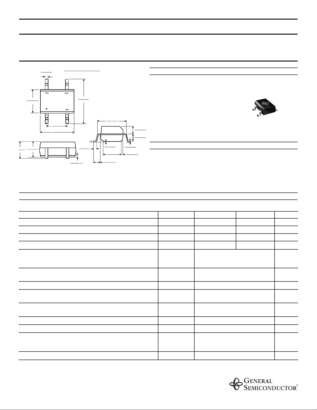
0.029 (0.74)
0.017 (0.43)
0-8
o
0.049 (1.24)
0.039 (0.99)
0.062 (1.57)
0.058 (1.47)
0.016 (0.41)
0.006 (0.15)
0.018 (0.46)
0.014 (0.36)
0.008 (0.20)
0.004 (0.10)
0.117 (2.97)
0.107 (2.72)
0.058 (1.47)
0.054 (1.37)
0.252 (6.40)
0.272 (6.90)
0.106 (2.70)
0.090 (2.30)
0.0075 (0.19)
0.0065 (0.16)
0.105 (2.67)
0.095 (2.41)
0.195 (4.95)
0.179 (4.55)
0.144 (3.65)
0.161 (4.10)
0.205 (5.21)
0.195 (4.95)
4 (2.90)
0.038 (0.96)
0.019 (0.48)
Case Style MBS
Dimensions in inches and (millimeters)
PATENT PENDING PATENT PENDING PATENT PENDING
9/8/98

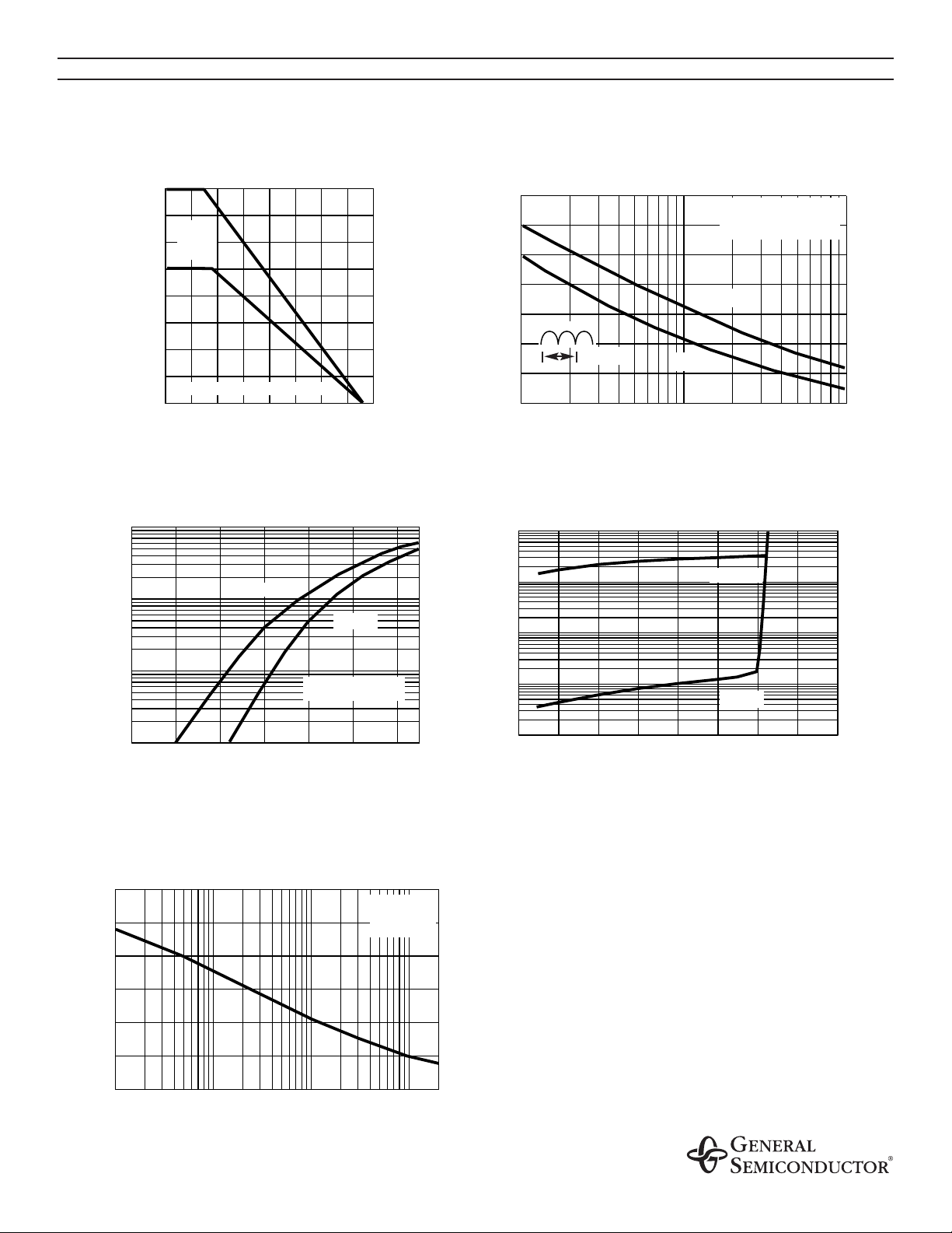
RATINGS AND CHARACTERISTIC CURVES RMB2S THRU RMB4S
FIG. 1 - DERATING CURVE FOR OUTPUT
RECTIFIED CURRENT
AMBIENT TEMPERATURE, °C
PEAK FORWARD SURGE CURRENT,
AMPERES
FIG. 2 - MAXIMUM NON-REPETITIVE PEAK FORWARD SURGE
CURRENT PER LEG
NUMBER OF CYCLES
AVERAGE FORWARD RECTIFIED CURRENT,
AMPERES
FIG. 3 - TYPICAL FORWARD VOLTAGE
CHARACTERISTICS PER LEG
FIG. 4 - TYPICAL REVERSE LEAKAGE CHARACTERISTICS
PER LEG
FIG. 5 - TYPICAL JUNCTION CAPACITANCE
PER LEG
INSTANTANEOUS FORWARD CURRENT,
AMPERES
INSTANTANEOUS REVERSE LEAKAGE CURRENT,
MICROAMPERES
JUNCTION CAPACITANCE, pF
INSTANTANEOUS FORWARD VOLTAGE,
VOLTS
PERCENT OF RATED PEAK REVERSE
VOLTAGE, %
REVERSE VOLTAGE, VOLTS
TA=40°C
SINGLE HALF SINE-WAVE
(JEDEC Method)
TJ=125°C
TJ=25°C
TJ=25°C
f=1.0 MHz
Vsig=50mVp-p
TJ=150°C
TJ=25°C
PULSE WIDTH=300µs
1% DUTY CYCLE
f=60 H
Z
f=50 H
Z
1.0 CYCLE
GLASS
EPOXY
P.C.B.
RESISTIVE OR INDUCTIVE LOAD
10
1
0.1
0.8
0.7
0.6
0.5
0.4
0.3
0.2
0.1
0
0 20 40 60 80 100 120 140 160
35
30
25
20
15
10
5.0
0
1
10
100
10
1
0.1
100
0.01
30
25
20
15
10
5.0
0
0.1
0.8
0.6
0.4
0.2
1
1.0 1.2
10
1.4
100
200
0.01
020
40
80 100 120 140 160
60
 Loading...